Project One Report
Project One Report
Project One Report

You also want an ePaper? Increase the reach of your titles
YUMPU automatically turns print PDFs into web optimized ePapers that Google loves.
<strong>Project</strong> <strong>One</strong> <strong>Report</strong><br />
Chris Barwick<br />
ECE 406 Section 1<br />
March 20 th 2008<br />
I. INTRODUCTION<br />
As digital systems become larger and more complex, it becomes increasingly<br />
difficult to organize, test, and debug. The development of hardware description<br />
languages (HDL) allows one to build an entire hardware system using a relatively<br />
simple programming language. <strong>Project</strong> one used the Verilog HDL to build a<br />
simplified version of the LC-3 microprocessor. The project not only taught me the<br />
Verilog language itself, but also how to deal with a complex system such as the LC-3<br />
by using a top down design style.<br />
The following report gives a basic overview of how I dealt with designing the<br />
LC-3 microprocessor. Section two summarizes how to take a complex digital system,<br />
break it up into smaller parts, and then implement those parts. Section three reviews<br />
the most difficult part of this project, debugging. Lessons learned from this project<br />
and conclusions are given in section five. Finally, an appendix is provided for some<br />
statistics about the project as well as the grading breakdown.<br />
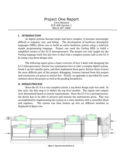
II. DESIGN PROCESS<br />
Since the LC-3 is a very complex system, a top down design style was used. In<br />
this style, the first step is to define the top level module. The inputs and outputs<br />
were determined based on system requirements. Since the LC-3 is a microprocessor,<br />
the device has to be able to process and execute the instructions given. This was<br />
accomplished by implementing the system as a state machine with a controller block<br />
and registers. The system was then broken up into six different modules as<br />
displayed in figure one.<br />
Figure 1: Top level view of the LC‐3
ECE 406: <strong>Project</strong> <strong>One</strong> <strong>Report</strong> Barwick<br />
Each of these modules were outlined with specific requirements. Once these<br />
requirements were defined, they were implemented as well as tested individually.<br />
For example, the Controller block, which keeps track of the different states of the<br />
system, was first outlined using a state diagram and then implemented in Verilog<br />
using a case statement and register.<br />
III. TESTING AND DEBUGGING<br />
Perhaps the most difficult part of this project was testing and debugging.<br />
After each module was designed, a test bench was written for that module to<br />
determine if the module met the requirements detailed in the design process.<br />
Testing each individual module first rather than waiting to test the entire system<br />
proved to be extremely helpful. It caught obvious bugs and prevented me from<br />
feeling overwhelmed. However, it turned out that testing the modules individually<br />
does not guarantee that the over system will function properly. Once the modules<br />
were connected together, there were several issues some of which have been outlined<br />
below.<br />
a. Improper connections<br />
When the microprocessor was first compiled, several errors were received<br />
stemming from the top level module. The specific error was:<br />
ncelab: *W,CUVMPW (./proj1.v,30|74): port sizes differ<br />
in port connection.<br />
The error resulted from not explicitly stating multiple wire labels that<br />
connect each module. If a single wire connects the modules, such as the “clock”,<br />
it does not need to be defined as a wire. However, if it is multiple wires, such as<br />
“D_Data”, the label needs to be defined (ex. “wire [47:0] D_Data;”). I defined<br />
the wires needed wires explicitly and the program complied without error.<br />
b. Bad Fetch Module<br />
After the system successfully compiled, the anomalous behavior shown in<br />
figure two was observed. The system did not seem to be getting the proper<br />
memory address, which is determined by the fetch module. The schematic for<br />
the fetch module was reevaluated and it was determined that the “pc” signal was<br />
not being set properly. During certain states the “pc” signal from the fetch<br />
module needed to be high impedance due to a shared bus. A simple change in the<br />
code within the fetch module fixed this. This obvious bug should have been<br />
caught during the individual module testing and may have gotten through due to<br />
poor testing.<br />
Page | 2
ECE 406: <strong>Project</strong> <strong>One</strong> <strong>Report</strong> Barwick<br />
Figure 2: Waveform resulting from a bad fetch module<br />
c. Bad Decode Module<br />
Once the Fetch module was fixed, the microprocessor functioned properly<br />
until it hit the STI instruction. Figure three displays the behavior. Since the LDI<br />
instruction, which is similar to STI, worked properly, the decode block was<br />
checked to make sure the proper control signals were being set. The actual<br />
control signals matched the control signals written down in class. After some<br />
more debugging, I noticed that the address the memory was receiving not correct.<br />
This address is provided by the MemAccess module, which also was receiving the<br />
incorrect address. The execute module was not providing the proper “pcout”<br />
address because the decode block set “PC sel 2” to choose VSR1. After talking<br />
with fellow students, it turns out that I copied the control signals down wrong.<br />
The decode block was corrected so that “PC sel 2” was set to npc for the STI<br />
instruction. After this fix, the microprocessor then functioned properly.<br />
Figure 3: Waveform resulting from a bad decode module<br />
Page | 3
ECE 406: <strong>Project</strong> <strong>One</strong> <strong>Report</strong> Barwick<br />
IV. LESSONS LEARNED AND CONCLUSION<br />
This project has provided some important lessons; including writing better<br />
individual module test benches and making sure the design requirements are<br />
correct. While it is difficult test each module exhaustively, it is better to put the time<br />
into debugging a single module rather than trying to find the bug once the system<br />
has been put together. Also, before trying to implement a design, ensure that you<br />
have the design requirements correct not only for the entire system, but for each<br />
module. This can save a lot of headaches when testing.<br />
This project has also provided some insight on how to deal with complex<br />
digital systems such as the LC-3 microprocessor. Using a top down design style can<br />
help one break up the problem into simple, manageable parts. The design technique<br />
used in this project can be scaled to bigger and much more complicated digital<br />
systems such as today CPUs. The techniques used are very similar to the techniques<br />
that companies such as Intel or AMD use when designing their complex processors.<br />
Page | 4
ECE 406: <strong>Project</strong> <strong>One</strong> <strong>Report</strong> Barwick<br />
Appendix<br />
ECE 406-001<br />
<strong>Project</strong> #1 Statistics<br />
Chris Barwick<br />
March 20, 2008<br />
Part 1: To be filled out by student<br />
Points Originality<br />
/ 4 Did you use the Controller from the HW#5 solution (yes/no)? - No<br />
/ 3 Did you use the Fetch Block from the HW#6 solution (yes/no)? – No<br />
/ 3 Did you use the Execute Block from the HW#6 solution (yes/no)? -No<br />
Points Synthesis Results<br />
/ 5 Number of logic elements: 319<br />
/ 5 Number of registers: 178<br />
/ 5 Number of tri-state buffers:34<br />
/ 5 Number of memory bits: 0<br />
/ 10 Please attach to the end of this report a print-out of all text from the Analysis and Synthesis<br />
Messages section of your .map.rpt file. If you have warnings and/or errors, please provide<br />
your best one- or two- sentence explanation for why each warning or error is occurring.<br />
/ 40 Total for Originality and Design Statistics<br />
Part 2: To be filled out by grader<br />
Points Execution graded by:<br />
/ 10 All modules included in proj1.v<br />
/ 10 Correct execution of proj1.dat<br />
/ 10 Correct execution of second program<br />
/ 30 Total for Wolfware submission<br />
Part 3: To be filled out by instructor<br />
Points Element<br />
/ 10 Technical Depth<br />
/ 10 Readability<br />
/ 10 Attractiveness<br />
/ 100 Total for <strong>Project</strong><br />
Page | 5
ECE 406: <strong>Project</strong> <strong>One</strong> <strong>Report</strong> Barwick<br />
+-------------------------------+<br />
; Analysis & Synthesis Messages ;<br />
+-------------------------------+<br />
Info: *******************************************************************<br />
Info: Running Quartus II Analysis & Synthesis<br />
Info: Version 7.2 Build 203 02/05/2008 Service Pack 2 SJ Web Edition<br />
Info: Processing started: Wed Mar 19 23:28:42 2008<br />
Info: Command: quartus_map --read_settings_files=on --write_settings_files=off proj1 -<br />
c proj1<br />
Info: Found 10 design units, including 10 entities, in source file proj1.v<br />
Info: Found entity 1: proj1<br />
Info: Found entity 2: Execute<br />
Info: Found entity 3: alu<br />
Info: Found entity 4: extension<br />
Info: Found entity 5: Controller<br />
Info: Found entity 6: Fetch<br />
Info: Found entity 7: MemAccess<br />
Info: Found entity 8: Writeback<br />
Info: Found entity 9: Decode<br />
Info: Found entity 10: RegFile<br />
Info: Elaborating entity "proj1" for the top level hierarchy<br />
Info: Elaborating entity "Fetch" for hierarchy "Fetch:f"<br />
Info: Elaborating entity "MemAccess" for hierarchy "MemAccess:memacc"<br />
Info: Elaborating entity "Controller" for hierarchy "Controller:cont"<br />
Info: Elaborating entity "Decode" for hierarchy "Decode:dec"<br />
Info: Elaborating entity "RegFile" for hierarchy "Decode:dec|RegFile:regf"<br />
/**These warnings are due to the assignment of the register, but the variable is not<br />
read in my code. These assignments were made to see what the registers contain in<br />
Simvision**/<br />
Warning (10036): Verilog HDL or VHDL warning at proj1.v(532): object "R0" assigned a<br />
value but never read<br />
Warning (10036): Verilog HDL or VHDL warning at proj1.v(532): object "R1" assigned a<br />
value but never read<br />
Warning (10036): Verilog HDL or VHDL warning at proj1.v(532): object "R2" assigned a<br />
value but never read<br />
Warning (10036): Verilog HDL or VHDL warning at proj1.v(532): object "R3" assigned a<br />
value but never read<br />
Warning (10036): Verilog HDL or VHDL warning at proj1.v(532): object "R4" assigned a<br />
value but never read<br />
Warning (10036): Verilog HDL or VHDL warning at proj1.v(532): object "R5" assigned a<br />
value but never read<br />
Warning (10036): Verilog HDL or VHDL warning at proj1.v(532): object "R6" assigned a<br />
value but never read<br />
Warning (10036): Verilog HDL or VHDL warning at proj1.v(532): object "R7" assigned a<br />
value but never read<br />
Info: Elaborating entity "Writeback" for hierarchy "Writeback:write"<br />
Info: Elaborating entity "Execute" for hierarchy "Execute:exe"<br />
Info: Elaborating entity "extension" for hierarchy "Execute:exe|extension:u1"<br />
Info: Elaborating entity "alu" for hierarchy "Execute:exe|alu:u2"<br />
Info: Generated suppressed messages file<br />
C:/Users/Chris/Desktop/PROJECT1/proj1.map.smsg<br />
Info: Implemented 501 device resources after synthesis - the final resource count<br />
might be different<br />
Info: Implemented 19 input pins<br />
Info: Implemented 33 output pins<br />
Info: Implemented 449 logic cells<br />
Info: Quartus II Analysis & Synthesis was successful. 0 errors, 8 warnings<br />
Info: Allocated 163 megabytes of memory during processing<br />
Info: Processing ended: Wed Mar 19 23:28:56 2008<br />
Info: Elapsed time: 00:00:14<br />
Page | 6