- Page 1 and 2:
Huang-Jen Chiu Dept. of Electronic
- Page 3 and 4:
� Power Electronic Systems Outlin
- Page 5 and 6:
Power Electronic Systems
- Page 7 and 8:
Switch-Mode Switch Mode Power Suppl
- Page 9 and 10:
Application in Adjustable Speed Dri
- Page 11 and 12:
Scope and Applications
- Page 13 and 14:
Power Processor as a Combination of
- Page 15 and 16:
AC Motor Drive • Converter 1 rect
- Page 17 and 18:
Interdisciplinary Nature of Power E
- Page 19 and 20:
Diodes • On and off states contro
- Page 21 and 22:
Thyristors • Semi-controlled devi
- Page 23 and 24:
Generic Switch Symbol • Idealized
- Page 25 and 26:
Bipolar Junction Transistors (BJT)
- Page 27 and 28:
MOSFETs • Easy to control by the
- Page 29 and 30:
GTO Turn-Off Turn Off • Need a tu
- Page 31 and 32:
MOS-Controlled MOS Controlled Thyri
- Page 33 and 34:
Summary of Device Capabilities
- Page 35 and 36:
Chapter 3 Review of Basic Electrica
- Page 37 and 38:
Three-Phase Three Phase Circuit
- Page 39 and 40:
Fourier Analysis ∞ 1 f(t) = F0 +
- Page 41 and 42:
Phasor Representation
- Page 43 and 44:
Inductor Voltage and Current in Ste
- Page 45 and 46:
Ampere’s Ampere s Law ∫ H dl =
- Page 47 and 48:
B-H H Relationship; Saturation •
- Page 49 and 50:
Concept of Magnetic Reluctance •
- Page 51 and 52:
Analogy between Equations in Electr
- Page 53 and 54:
Inductance L • Inductance relates
- Page 55 and 56:
Transformer Equivalent Circuit
- Page 57 and 58: Chapter 4 Computer Simulation
- Page 59 and 60: Large-Signal Large Signal System Si
- Page 61 and 62: Closed-Loop Closed Loop Operation:
- Page 63 and 64: Modeling of a Simple Converter ⎡
- Page 65 and 66: PSpice-based PSpice based Simulatio
- Page 67 and 68: Chapter 5 Diode Rectifiers
- Page 69 and 70: A Simple Circuit • Resistive load
- Page 71 and 72: A Simple Circuit (Load has a dc bac
- Page 73 and 74: Diode-Rectifier Diode Rectifier Bri
- Page 75 and 76: Current Commutation • Assuming in
- Page 77 and 78: Current Commutation in Full-Bridge
- Page 79 and 80: Rectifier with a dc-side dc side vo
- Page 81 and 82: Diode Rectifier Bridge • Equivale
- Page 83 and 84: Input Line-Current Line Current Dis
- Page 85 and 86: Line-Voltage Line Voltage Distortio
- Page 87 and 88: A Three-Phase, Three Phase, Four-Wi
- Page 89 and 90: Three-Phase, Three Phase, Full-Brid
- Page 91 and 92: Rectifier with a Large Filter Capac
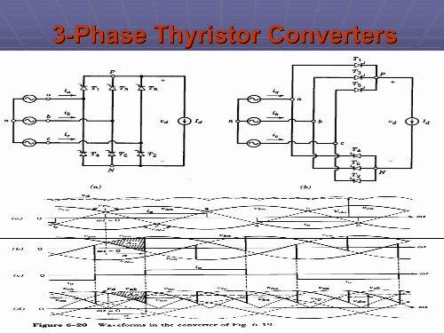
- Page 93 and 94: Chapter 6 Thyristor Converters •
- Page 95 and 96: Primitive circuits with thyristors
- Page 97 and 98: Full-Bridge Full Bridge Thyristor C
- Page 99 and 100: Average DC Output Voltage is s1 s3
- Page 101 and 102: 1-Phase Phase Thyristor Converter
- Page 103 and 104: DC Voltage versus Load Current •
- Page 105 and 106: Thyristor Converters: Inverter Mode
- Page 107: Thyristor Converters: Inverter Mode
- Page 112 and 113: Block Diagram of DC-DC DC DC Conver
- Page 114 and 115: Pulse-Width Pulse Width Modulation
- Page 116 and 117: Waveforms at the boundary of Cont./
- Page 118 and 119: Limits of Cont./ Discont. Discont.
- Page 120 and 121: d Step-Up Step Up DC-DC DC DC Conve
- Page 122 and 123: D = 4 27 V V o d V ( V Discont. Dis
- Page 124 and 125: Output Ripple ΔV o = I o t C on =
- Page 126 and 127: Limits of Cont./ Discont. Discont.
- Page 128 and 129: V o V d Limits of Cont./ Discont. D
- Page 130 and 131: • The output voltage can be highe
- Page 132 and 133: Converter Waveforms
- Page 134 and 135: Switch Utilization in DC-DC DC DC C
- Page 136 and 137: Chapter 8 Switch-Mode Switch Mode D
- Page 138 and 139: Switch-Mode Switch Mode DC-AC DC AC
- Page 140 and 141: Details of a Switching Time Period
- Page 142 and 143: Harmonics due to Over-modulation Ov
- Page 144 and 145: Half-Bridge Half Bridge Inverter
- Page 146 and 147: PWM to Synthesize Sinusoidal Output
- Page 148 and 149: DC-Side DC Side Current
- Page 150 and 151: DC-Side DC Side Current in a Single
- Page 152 and 153: Square-Wave Square Wave and PWM Ope
- Page 154 and 155: Three-Phase Three Phase Inverter
- Page 156 and 157: Three-Phase Three Phase Inverter Ha
- Page 158 and 159:
Square-Wave Square Wave and PWM Ope
- Page 160 and 161:
Effect of Blanking Time • Results
- Page 162 and 163:
Effect of Blanking Time • Effect
- Page 164 and 165:
Tolerance-Band Tolerance Band Curre
- Page 166 and 167:
Chapter 9 Zero-Voltage Zero Voltage
- Page 168 and 169:
Turn-on Turn on and Turn-off Turn o
- Page 170 and 171:
Undamped Undamped Series Series-Res
- Page 172 and 173:
Impedance of a Series-Resonant Seri
- Page 174 and 175:
Impedance of a Parallel-Resonant Pa
- Page 176 and 177:
SLR Converter Waveforms 1/2ωo
- Page 178 and 179:
Lossless Snubbers in SLR Converters
- Page 180 and 181:
SLR Converter Control • The opera
- Page 182 and 183:
No PLR Converter Waveforms turn - o
- Page 184 and 185:
PLR Converter Characteristics • O
- Page 186 and 187:
Parallel-Resonant Parallel Resonant
- Page 188 and 189:
Single-switch ZCS Turn-on Class-E C
- Page 190 and 191:
Resonant Switch Converters
- Page 192 and 193:
ZCS Turn-on ZCS Resonant-Switch Res
- Page 194 and 195:
MOSFET Internal Capacitances ZVS is
- Page 196 and 197:
ZVS-CV ZVS CV DC-DC DC DC Converter
- Page 198 and 199:
Three-Phase Three Phase ZVS-CV ZVS
- Page 200 and 201:
ZVS-CV ZVS CV with Voltage Cancella
- Page 202 and 203:
Three-Phase Three Phase Resonant DC
- Page 204 and 205:
High-Frequency High Frequency-Link
- Page 206 and 207:
Chapter 10 Switching DC Power Suppl
- Page 208 and 209:
Switching DC Power Supply • High
- Page 210 and 211:
Transformer Analysis • Needed to
- Page 212 and 213:
Flyback Converter • Derived from
- Page 214 and 215:
Flyback Converter • Switching wav
- Page 216 and 217:
Forward Converter • Derived from
- Page 218 and 219:
Forward Converter: Other Possible T
- Page 220 and 221:
Half-Bridge Half Bridge Converter
- Page 222 and 223:
Current-Source Current Source Conve
- Page 224 and 225:
Core Utilization in Various Convert
- Page 226 and 227:
⎪⎩ ⎪ ⎨ ⎧ − + = + = •
- Page 228 and 229:
• Linearization of the Power Stag
- Page 230 and 231:
R >> r + ) ⇒ ( C rL v o = R( x 1
- Page 232 and 233:
Forward Converter: Transfer Functio
- Page 234 and 235:
Linearizing the PWM Block ~ d( s) 1
- Page 236 and 237:
A General Amplifier for Error Compe
- Page 238 and 239:
Feedback-Loop Feedback Loop Stabili
- Page 240 and 241:
Feedback-Loop Feedback Loop Stabili
- Page 242 and 243:
Compensator Design Example G m = G
- Page 244 and 245:
Voltage Feed-Forward Feed Forward
- Page 246 and 247:
Various Types of Current Mode Contr
- Page 248 and 249:
A Typical PWM Control IC
- Page 250 and 251:
Implementing Electrical Isolation i
- Page 252 and 253:
Input Filter • Needed to comply w
- Page 254 and 255:
Chapter 11 Power Conditioners and U
- Page 256 and 257:
Typical Voltage Tolerance Envelope
- Page 258 and 259:
Electronic Tap Changers • Control
- Page 260 and 261:
UPS: Possible Rectifier Arrangement
- Page 262 and 263:
UPS: Another Possible Input Arrange
- Page 264 and 265:
UPS: Various Inverter Arrangements
- Page 266 and 267:
UPS Supplying Several Loads • Wit
- Page 268 and 269:
UPS: Using the Line Voltage as Back
- Page 270 and 271:
Inductive Ballast of Fluorescent La
- Page 272 and 273:
Electronic Ballast for Fluorescent
- Page 274 and 275:
Industrial Induction Heating • Ne
- Page 276 and 277:
Switch-Mode Switch Mode Welders •
- Page 278 and 279:
HVDC Transmission • There are man
- Page 280 and 281:
HVDC Transmission: AC-Side AC Side
- Page 282 and 283:
Thyristor-Controlled Thyristor Cont
- Page 284 and 285:
Instantaneous VAR Controller (SATCO
- Page 286 and 287:
Photovoltaic Interface • This sch
- Page 288 and 289:
Active Filters for Harmonic Elimina
- Page 290 and 291:
Various Loads Supplied by the Utili
- Page 292 and 293:
Typical Harmonics in the Input Curr
- Page 294 and 295:
Harmonic Guidelines: IEEE 519 • L
- Page 296 and 297:
Power-Factor Power Factor-Correctio
- Page 298 and 299:
Power-Factor Power Factor-Correctio
- Page 300 and 301:
Switch-Mode Switch Mode Converter C
- Page 302 and 303:
EMI: Conducted Interefence • Comm
- Page 304 and 305:
Conducted EMI • Various Standards
- Page 306 and 307:
V d - + i D F D f Turn-off Turn off
- Page 308 and 309:
Aspects of EMC (EMI、EMS) (EMI EMS
- Page 310 and 311:
Three Ways to Prevent Interference
- Page 312 and 313:
Other Aspects of EMC
- Page 314 and 315:
Frequency Range of EMC Requirements
- Page 316 and 317:
Federal Communications Commission (
- Page 318 and 319:
FCC Emission for Class A
- Page 320 and 321:
Open Area Test Site
- Page 322 and 323:
Radiated EMI Test Setup
- Page 324 and 325:
Conducted EMI Test Setup
- Page 326 and 327:
Conducted Emissions Test Layout
- Page 328 and 329:
CISPR Bandwidth Requirements
- Page 330 and 331:
Design Constraints for Products �
- Page 332 and 333:
Effects of Component Leads
- Page 334 and 335:
1000Ω, Carbon Resistor having 1/4
- Page 336 and 337:
470 pF Ceramic Capacitor with Short
- Page 338 and 339:
0.15 μF Tantalum Capacitor with Sh
- Page 340 and 341:
Inductors
- Page 342 and 343:
Common-Mode Common Mode Choke
- Page 344 and 345:
Frequency Response of the Relative
- Page 346 and 347:
Multi-Turn Multi Turn Ferrite Beads
- Page 348 and 349:
The Periodic, Trapezoidal Pulse Tra
- Page 350 and 351:
Spectrum Analyzer
- Page 352 and 353:
The Effects of Differential-Mode Cu
- Page 354 and 355:
Radiated Emission due to the Differ
- Page 356 and 357:
Common-Mode Current Emission | E C
- Page 358 and 359:
Susceptibility Models
- Page 360 and 361:
Measurement of Conducted Emissions
- Page 362 and 363:
Differential-Mode and Common-Mode C
- Page 364 and 365:
Definition of the Insertion Loss of
- Page 366 and 367:
Insertion Loss Tests
- Page 368 and 369:
Common-Mode Common Mode Choke
- Page 370 and 371:
The Equivalent Circuit of the Filte
- Page 372 and 373:
A Device to Separate the CM and DM
- Page 374 and 375:
Measured Conducted Emissions with 3
- Page 376 and 377:
Measured Conducted Emissions with a
- Page 378 and 379:
Nonideal Effects in Diodes
- Page 380 and 381:
The Effect of Primary-to Primary to
- Page 382 and 383:
Crosstalk � The unintended EM cou
- Page 384 and 385:
Wire-type Wire type Line illustrati
- Page 386 and 387:
The Equivalent Circuit of TEM Wave
- Page 388 and 389:
Frequency Response of the Crosstalk
- Page 390 and 391:
Common-impedance Common impedance C
- Page 392 and 393:
Time-Domain Time Domain Crosstalk f
- Page 394 and 395:
The Lumped Equivalent Circuit for V
- Page 396 and 397:
The Lumped Equivalent Circuit ^ V I
- Page 398 and 399:
Twisted Wires
- Page 400 and 401:
Terminating a Twisted Pair
- Page 402 and 403:
Explanation of the Effect of an Unb
- Page 404 and 405:
A Coupling Model for the Balanced T
- Page 406 and 407:
Purposes of a Shield � To prevent
- Page 408 and 409:
Termination of a Cable Shield � T
- Page 410 and 411:
R dB ≅ Reflection Loss 20 log 10
- Page 412 and 413:
Shielding Effectiveness
- Page 414 and 415:
Shielding Effectiveness of Metals
- Page 416 and 417:
The Frequency Dependence of Various
- Page 418 and 419:
The Bands to Reduced the Magnetic F
- Page 420 and 421:
ESD Events � Typical rise times a
- Page 422 and 423:
Three Techniques for Preventing Pro
- Page 424 and 425:
Hardware Immunity � Secondary arc
- Page 426 and 427:
Single-point Single point Ground
- Page 428 and 429:
The Methods of Preventing ESD-induc
- Page 430 and 431:
Reduction of Loop Areas to Reduce t
- Page 432 and 433:
Packaging Consideration � A criti
- Page 434 and 435:
The Effect of Conductor Inductance
- Page 436 and 437:
Ground Problems between Analog and
- Page 438 and 439:
Methods for Decoupling Subsystems
- Page 440 and 441:
Use of Interspersed Grounds to Redu
- Page 442 and 443:
Decoupling Subsystems � Common-mo
- Page 444 and 445:
Component Placement
- Page 446 and 447:
A Good Layout for a Typical Digital
- Page 448 and 449:
Unintentional Coupling of Signals b
- Page 450 and 451:
Decoupling Capacitor Placement