- Page 1 and 2:
Huang-Jen Chiu Dept. of Electronic
- Page 3 and 4:
� Power Electronic Systems Outlin
- Page 5 and 6:
Power Electronic Systems
- Page 7 and 8:
Switch-Mode Switch Mode Power Suppl
- Page 9 and 10:
Application in Adjustable Speed Dri
- Page 11 and 12:
Scope and Applications
- Page 13 and 14:
Power Processor as a Combination of
- Page 15 and 16:
AC Motor Drive • Converter 1 rect
- Page 17 and 18: Interdisciplinary Nature of Power E
- Page 19 and 20: Diodes • On and off states contro
- Page 21 and 22: Thyristors • Semi-controlled devi
- Page 23 and 24: Generic Switch Symbol • Idealized
- Page 25 and 26: Bipolar Junction Transistors (BJT)
- Page 27 and 28: MOSFETs • Easy to control by the
- Page 29 and 30: GTO Turn-Off Turn Off • Need a tu
- Page 31 and 32: MOS-Controlled MOS Controlled Thyri
- Page 33 and 34: Summary of Device Capabilities
- Page 35 and 36: Chapter 3 Review of Basic Electrica
- Page 37 and 38: Three-Phase Three Phase Circuit
- Page 39 and 40: Fourier Analysis ∞ 1 f(t) = F0 +
- Page 41 and 42: Phasor Representation
- Page 43 and 44: Inductor Voltage and Current in Ste
- Page 45 and 46: Ampere’s Ampere s Law ∫ H dl =
- Page 47 and 48: B-H H Relationship; Saturation •
- Page 49 and 50: Concept of Magnetic Reluctance •
- Page 51 and 52: Analogy between Equations in Electr
- Page 53 and 54: Inductance L • Inductance relates
- Page 55 and 56: Transformer Equivalent Circuit
- Page 57 and 58: Chapter 4 Computer Simulation
- Page 59 and 60: Large-Signal Large Signal System Si
- Page 61 and 62: Closed-Loop Closed Loop Operation:
- Page 63 and 64: Modeling of a Simple Converter ⎡
- Page 65 and 66: PSpice-based PSpice based Simulatio
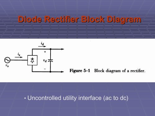
- Page 67: Chapter 5 Diode Rectifiers
- Page 71 and 72: A Simple Circuit (Load has a dc bac
- Page 73 and 74: Diode-Rectifier Diode Rectifier Bri
- Page 75 and 76: Current Commutation • Assuming in
- Page 77 and 78: Current Commutation in Full-Bridge
- Page 79 and 80: Rectifier with a dc-side dc side vo
- Page 81 and 82: Diode Rectifier Bridge • Equivale
- Page 83 and 84: Input Line-Current Line Current Dis
- Page 85 and 86: Line-Voltage Line Voltage Distortio
- Page 87 and 88: A Three-Phase, Three Phase, Four-Wi
- Page 89 and 90: Three-Phase, Three Phase, Full-Brid
- Page 91 and 92: Rectifier with a Large Filter Capac
- Page 93 and 94: Chapter 6 Thyristor Converters •
- Page 95 and 96: Primitive circuits with thyristors
- Page 97 and 98: Full-Bridge Full Bridge Thyristor C
- Page 99 and 100: Average DC Output Voltage is s1 s3
- Page 101 and 102: 1-Phase Phase Thyristor Converter
- Page 103 and 104: DC Voltage versus Load Current •
- Page 105 and 106: Thyristor Converters: Inverter Mode
- Page 107 and 108: Thyristor Converters: Inverter Mode
- Page 111 and 112: Chapter 7 DC-DC DC DC Switch-Mode S
- Page 113 and 114: Stepping Down a DC Voltage • A si
- Page 115 and 116: d o Step-Down Step Down DC-DC DC DC
- Page 117 and 118: Step-Down Step Down DC-DC DC DC Con
- Page 119 and 120:
ΔQ Δ Vo = = C Output Voltage Ripp
- Page 121 and 122:
Limits of Cont./ Discont. Discont.
- Page 123 and 124:
V V o d Limits of Cont./ Discont. D
- Page 125 and 126:
Step-Down/Up Step Down/Up DC-DC DC
- Page 127 and 128:
Discontinuous Conduction Mode V D =
- Page 129 and 130:
Output Voltage Ripple • ESR is as
- Page 131 and 132:
Converter for DC-Motor DC Motor Dri
- Page 133 and 134:
Output Ripple in Converters for DC-
- Page 135 and 136:
Reversing the Power Flow in DC-DC D
- Page 137 and 138:
Switch-Mode Switch Mode DC-AC DC AC
- Page 139 and 140:
V m = a m = f Synthesis of a Sinuso
- Page 141 and 142:
Harmonics in the DC-AC DC AC Invert
- Page 143 and 144:
Square-Wave Square Wave Mode of Ope
- Page 145 and 146:
Single-Phase Single Phase Full-Brid
- Page 147 and 148:
Analysis assuming Fictitious Filter
- Page 149 and 150:
Uni-polar Uni polar Voltage Switchi
- Page 151 and 152:
Sinusoidal Synthesis by Voltage Shi
- Page 153 and 154:
Push-Pull Push Pull Inverter • On
- Page 155 and 156:
Three-Phase Three Phase PWM Wavefor
- Page 157 and 158:
Three-Phase Three Phase Inverter Ou
- Page 159 and 160:
DC-Side DC Side Current in a Three-
- Page 161 and 162:
Effect of Blanking Time ΔV o ⎧ 2
- Page 163 and 164:
Programmed Harmonic Elimination •
- Page 165 and 166:
Fixed-Frequency Fixed Frequency Ope
- Page 167 and 168:
Hard Switching Waveforms • The ou
- Page 169 and 170:
Switching Trajectories • Comparis
- Page 171 and 172:
Series Series-Resonant Circuit Reso
- Page 173 and 174:
Undamped Undamped Parallel Parallel
- Page 175 and 176:
Series-Loaded Series Loaded Resonan
- Page 177 and 178:
ZVS, ZCS SLR Converter Waveforms ω
- Page 179 and 180:
SLR Converter Characteristics • T
- Page 181 and 182:
ZCS Parallel-Loaded Parallel Loaded
- Page 183 and 184:
No ZVS PLR Converter Waveforms turn
- Page 185 and 186:
Hybrid-Resonant Hybrid Resonant DC-
- Page 187 and 188:
Parallel-Resonant Parallel Resonant
- Page 189 and 190:
Class-E Class E Converters
- Page 191 and 192:
ZCS Turn-on ZCS Resonant-Switch Res
- Page 193 and 194:
ZVS Resonant-Switch Resonant Switch
- Page 195 and 196:
ZVS-CV ZVS CV DC-DC DC DC Converter
- Page 197 and 198:
ZVS-CV ZVS CV Principle Applied to
- Page 199 and 200:
Output Regulation by Voltage Contro
- Page 201 and 202:
Resonant DC-Link DC Link Inverter
- Page 203 and 204:
High-Frequency High Frequency-Link
- Page 205 and 206:
High-Frequency High Frequency-Link
- Page 207 and 208:
Linear Power Supplies • Very poor
- Page 209 and 210:
Switching DC Power Supply: Multiple
- Page 211 and 212:
PWM to Regulate Output
- Page 213 and 214:
Flyback Converter • Switch on and
- Page 215 and 216:
Other Flyback Converter Topologies
- Page 217 and 218:
Forward Converter: in Practice •
- Page 219 and 220:
Push-Pull Push Pull Inverter • Le
- Page 221 and 222:
Full-Bridge Full Bridge Converter
- Page 223 and 224:
Ferrite Core Material • Several m
- Page 225 and 226:
Control to Regulate Voltage Output
- Page 227 and 228:
Linearization of the Power Stage Li
- Page 229 and 230:
Forward Converter: An Example Forwa
- Page 231 and 232:
⎥ ⎥ ⎥ ⎦ ⎤ ⎢ ⎢ ⎢ ⎣
- Page 233 and 234:
Flyback Converter: Transfer Functio
- Page 235 and 236:
Typical Gain and Phase Plots of the
- Page 237 and 238:
Type-2 Type 2 Error Amplifier • S
- Page 239 and 240:
Feedback-Loop Feedback Loop Stabili
- Page 241 and 242:
L C F F o o o esr = Compensator Des
- Page 243 and 244:
F 1 Fco = Fs 5 z F F co esr EA = Co
- Page 245 and 246:
Voltage versus Current Mode Control
- Page 247 and 248:
Peak Current Mode Control • Slope
- Page 249 and 250:
Current Limiting
- Page 251 and 252:
Implementing Electrical Isolation i
- Page 253 and 254:
ESR of the Output Capacitor • ESR
- Page 255 and 256:
Distortion in the Input Voltage •
- Page 257 and 258:
Typical Range of Input Power Qualit
- Page 259 and 260:
Uninterruptible Power Supplies (UPS
- Page 261 and 262:
UPS: Another Possible Rectifier Arr
- Page 263 and 264:
Battery Charging Waveforms as Funct
- Page 265 and 266:
UPS: Control • Typically the load
- Page 267 and 268:
Another Possible UPS Arrangement
- Page 269 and 270:
Chapter 16 Residential and Industri
- Page 271 and 272:
Rapid-Start Rapid Start Fluorescent
- Page 273 and 274:
Induction Cooking • Pan is heated
- Page 275 and 276:
Welding Application
- Page 277 and 278:
Chapter 17 Electric Utility Applica
- Page 279 and 280:
Control of HVDC Transmission System
- Page 281 and 282:
Effect of Reactive Power on Voltage
- Page 283 and 284:
Thyristor-Switched Thyristor Switch
- Page 285 and 286:
Characteristics of Solar Cells •
- Page 287 and 288:
Harnessing of Wing Energy • A swi
- Page 289 and 290:
Chapter 18 Utility Interface • Po
- Page 291 and 292:
Diode-Rectifier Diode Rectifier Bri
- Page 293 and 294:
Harmonic Guidelines: IEEE 519 • C
- Page 295 and 296:
Reducing the Input Current Distorti
- Page 297 and 298:
Power-Factor Power Factor-Correctio
- Page 299 and 300:
Switch-Mode Switch Mode Converter I
- Page 301 and 302:
Switch-Mode Switch Mode Converter I
- Page 303 and 304:
Switching Waveforms • Typical ris
- Page 305 and 306:
Conducted EMI Filter
- Page 307 and 308:
+ V d - D f L s S w I o R Ls D Ls T
- Page 309 and 310:
EMI Sources and Sensors
- Page 311 and 312:
Four Basic EMC Problems
- Page 313 and 314:
EMC Requirements �� Those requi
- Page 315 and 316:
National Regulations Summary
- Page 317 and 318:
FCC Emission for Class B
- Page 319 and 320:
Comparison of the FCC Class A and C
- Page 321 and 322:
Chamber for Measurement of Radiated
- Page 323 and 324:
Antennas
- Page 325 and 326:
Line Impedance Stabilization Networ
- Page 327 and 328:
Conducted Emissions Test Layout
- Page 329 and 330:
Envelope Detector Quasi-Peak Detect
- Page 331 and 332:
Advantages of EMC Design � Minimi
- Page 333 and 334:
Resistors
- Page 335 and 336:
Capacitors
- Page 337 and 338:
470 pF Ceramic Capacitor with 1/2 I
- Page 339 and 340:
0.15 μF Tantalum Capacitor with 1/
- Page 341 and 342:
1.2μH Inductor
- Page 343 and 344:
Common-Mode Common Mode Choke
- Page 345 and 346:
Ferrite Beads
- Page 347 and 348:
Driver Circuit of the DC Motor
- Page 349 and 350:
The Spectra of 1V, 10MHz, 50% Duty
- Page 351 and 352:
The Effect of Bandwidth on Spectrum
- Page 353 and 354:
Differential-Mode Current Emission
- Page 355 and 356:
Common Mistakes that Lead to Unnece
- Page 357 and 358:
Radiated Emission due to the Common
- Page 359 and 360:
10V/m, 100MHz Incident Uniform Plan
- Page 361 and 362:
Line Impedance Stabilization Networ
- Page 363 and 364:
Methods of Reducing the Common-Mode
- Page 365 and 366:
Four Simple Filters V L , wo ω L I
- Page 367 and 368:
Conducted EMI Filter
- Page 369 and 370:
The Equivalent Circuit of the Filte
- Page 371 and 372:
The Dominant Component of Conducted
- Page 373 and 374:
Measured Conducted Emissions withou
- Page 375 and 376:
Measured Conducted Emissions with a
- Page 377 and 378:
Measured Conducted Emissions with a
- Page 379 and 380:
Construction of Transformers
- Page 381 and 382:
The Proper Filter Placement in the
- Page 383 and 384:
Three-Conductor Three Conductor Tra
- Page 385 and 386:
PCB Transmission Lines illustrating
- Page 387 and 388:
The Simple Inductive-Capacitive Ind
- Page 389 and 390:
Effect of Load Impedance
- Page 391 and 392:
Time-Domain Time Domain Crosstalk f
- Page 393 and 394:
The Capacitance Equivalent for the
- Page 395 and 396:
Illustration of Placing a Shield on
- Page 397 and 398:
Explanation of the Effect of Shield
- Page 399 and 400:
The Inductive-Capacitive Inductive
- Page 401 and 402:
A Model for the Unbalanced Twisted
- Page 403 and 404:
The Three Levels of Reducing Induct
- Page 405 and 406:
The Effect of Balanced and Unbalanc
- Page 407 and 408:
Degradation of Shielding Effectiven
- Page 409 and 410:
dB Shielding Effectiveness SE = R +
- Page 411 and 412:
Absorption Loss t / δ AdB = 20 log
- Page 413 and 414:
Shielding Effectiveness � Reflect
- Page 415 and 416:
The Methods of Shielding against Lo
- Page 417 and 418:
The Phenomenon of Saturation of Fer
- Page 419 and 420:
Effects of Apertures Since it is no
- Page 421 and 422:
Effects of the ESD Events � The i
- Page 423 and 424:
Preventing the ESD Event � Electr
- Page 425 and 426:
Preventing the Secondary Arc Discha
- Page 427 and 428:
Use of Shielded Cables to Exclude E
- Page 429 and 430:
Reduction of Loop Area in Power Dis
- Page 431 and 432:
Software Immunity � Watchdog rout
- Page 433 and 434:
Common-impedance Common impedance C
- Page 435 and 436:
Segregation of Grounds
- Page 437 and 438:
The Generation and Blocking of CM C
- Page 439 and 440:
Interconnection and Number of PCBs
- Page 441 and 442:
PCB and Subsystem Placement Attenti
- Page 443 and 444:
Splitting Crystal/ Oscillator Frequ
- Page 445 and 446:
Component Placement
- Page 447 and 448:
Creation of a Quiet Ground where Co
- Page 449 and 450:
Use of Decoupling Capacitors
- Page 451:
Minimizing the Loop Area of the Pow