Tune that dial - Index of
Tune that dial - Index of
Tune that dial - Index of

Create successful ePaper yourself
Turn your PDF publications into a flip-book with our unique Google optimized e-Paper software.
TECHNOLOGY READER CIRCUITS<br />
ured as an input, which also means <strong>that</strong><br />
an internal pull-up resistor is connected<br />
to the pin. The capacitor is charged via<br />
this resistor, but the charging time constant<br />
is much longer than the processor<br />
speed. During the interval when the<br />
input is still low, the value <strong>of</strong> the key is<br />
changed in rapid succession by a certain<br />
algorithm. This continues until the<br />
capacitor is fully charged. The input<br />
read as a ‘1’ at this point, at which time<br />
the key value stops changing. This<br />
results in a key with a random value.<br />
The randomness arises from the fact<br />
<strong>that</strong> the charging process is slow relative<br />
to the processor speed. The charging<br />
time corresponds to approximately<br />
10,000 processor cycles. Tests have<br />
shown <strong>that</strong> the charging time is not<br />
entirely constant. A 0.01-percent<br />
change in the charging time is sufficient<br />
to yield a different result. This<br />
also shows <strong>that</strong> two different transmitters<br />
will never generate the same key,<br />
especially because most capacitors<br />
have a tolerance <strong>of</strong> around 5%.<br />
With a normal start-up process<br />
(switching on power), the transmitter<br />
first reads the key present in memory,<br />
but it cannot be transmitted just like<br />
<strong>that</strong>. A preamble with a duty cycle <strong>of</strong><br />
exactly 50% is transmitted first to allow<br />
the operating point <strong>of</strong> the data slicer to<br />
be adjusted. The transitions in the preamble<br />
also serve to synchronise the<br />
timing at the receiver end with the timing<br />
at the transmitter end. A start bit<br />
is transmitted after the preamble to<br />
indicate <strong>that</strong> the key will be transmitted<br />
next. The ‘real’ data is only sent<br />
after the start bit, after which the<br />
transmitter is switched <strong>of</strong>f immediately<br />
and the microcontroller enters the<br />
power-down mode to minimise battery<br />
consumption.<br />
A different program is naturally necessary<br />
at the receiver end. In contrast to<br />
the transmitter, the receiver is always<br />
on. In this case the microcontroller listens<br />
to see whether anything is being<br />
received. If it is, it checks whether the<br />
received data stream has the correct<br />
format, which includes checking<br />
whether the start bit synchronisation<br />
is valid. After this it reads the key and<br />
compares it with the value <strong>of</strong> the key<br />
stored in its EEPROM memory.<br />
The microcontroller has a jumper <strong>that</strong><br />
enables it to read the key. If the jumper<br />
is fitted, the receiver is in ‘learn mode’.<br />
If a key is received in this mode, it is<br />
stored in the EEPROM. This means<br />
<strong>that</strong> the first time the receiver is<br />
switched on, the jumper must be fitted<br />
40<br />
and the code transmitted using the key<br />
transmitter so the key can be stored in<br />
the receiver’s memory. After the<br />
jumper is removed, the receiver should<br />
switch its outputs when the key transmitter<br />
is activated. It may be necessary<br />
to disconnect the receiver<br />
antenna for this procedure and activate<br />
the transmitter close to the receiver.<br />
This will reduce the effect <strong>of</strong> any interference<br />
signals present at 433.92 MHz.<br />
The watchdog timer is also enabled in<br />
the microcontroller on the receiver end.<br />
If the program counter is affected by a<br />
noise pulse on the supply line, for<br />
instance, which can lead to a ‘hung’<br />
system, the microcontroller will be<br />
reset automatically after approximately<br />
1 second and the receiver will execute<br />
a normal start-up.<br />
Data slicer and Manchester coding<br />
The data slicer in the receiver is built<br />
around an opamp in the receiver IC<br />
<strong>that</strong> is intended to be used for this purpose.<br />
A data slicer is simply a comparator<br />
with a reference level <strong>that</strong> is automatically<br />
set when a data signal with<br />
a duty cycle <strong>of</strong> 50% is received. It is<br />
thus important <strong>that</strong> the duty cycle <strong>of</strong><br />
the data signal is in fact 50%. Manchester<br />
coding is used to achieve this result.<br />
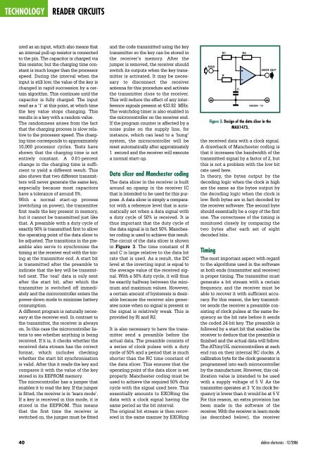
The circuit <strong>of</strong> the data slicer is shown<br />
in Figure 3. The time constant <strong>of</strong> R<br />
and C is large relative to the data bit<br />
rate <strong>that</strong> is used. As a result, the DC<br />
level at the inverting input is equal to<br />
the average value <strong>of</strong> the received signal.<br />
With a 50% duty cycle, it will thus<br />
be exactly halfway between the minimum<br />
and maximum values. However,<br />
a certain amount <strong>of</strong> hysteresis is desirable<br />
because the receiver also generates<br />
noise when no signal is present or<br />
the signal is relatively weak. This is<br />
provided by Rl and R2.<br />
It is also necessary to have the transmitter<br />
send a preamble before the<br />
actual data. The preamble consists <strong>of</strong><br />
a series <strong>of</strong> clock pulses with a duty<br />
cycle <strong>of</strong> 50% and a period <strong>that</strong> is much<br />
shorter than the RC time constant <strong>of</strong><br />
the data slicer. This ensures <strong>that</strong> the<br />
operating point <strong>of</strong> the data slicer is set<br />
properly. Manchester coding must be<br />
used to achieve the required 50% duty<br />
cycle with the signal used here. This<br />
essentially amounts to EXORing the<br />
data with a clock signal having the<br />
same period as the bit interval.<br />
The original bit stream is then recovered<br />
in the same manner by EXORing<br />
RSSI<br />
R1<br />
R<br />
C<br />
the received data with a clock signal.<br />
A drawback <strong>of</strong> Manchester coding is<br />
<strong>that</strong> it increases the bandwidth <strong>of</strong> the<br />
transmitted signal by a factor <strong>of</strong> 2, but<br />
this is not a problem with the low bit<br />
rate used here.<br />
In theory, the bytes output by the<br />
decoding logic when the clock is high<br />
are the same as the bytes output by<br />
the decoding logic when the clock is<br />
low. Both bytes are in fact decoded by<br />
the receiver s<strong>of</strong>tware. The second byte<br />
should essentially be a copy <strong>of</strong> the first<br />
one. The correctness <strong>of</strong> the timing is<br />
monitored closely by comparing the<br />
two bytes after each set <strong>of</strong> eight<br />
decoded bits.<br />
Timing<br />
The most important aspect with regard<br />
to the algorithms used in the s<strong>of</strong>tware<br />
at both ends (transmitter and receiver)<br />
is proper timing. The transmitter must<br />
generate a bit stream with a certain<br />
frequency, and the receiver must be<br />
able to recover it with sufficient accuracy.<br />
For this reason, the key transmitter<br />
sends the receiver a preamble consisting<br />
<strong>of</strong> clock pulses at the same frequency<br />
as the bit rate before it sends<br />
the coded 24-bit key. The preamble is<br />
followed by a start bit <strong>that</strong> enables the<br />
receiver to deduce <strong>that</strong> the preamble is<br />
finished and the actual data will follow.<br />
The ATtiny15L microcontrollers at each<br />
end run on their internal RC clocks. A<br />
calibration byte for the clock generator is<br />
programmed into each microcontroller<br />
by the manufacturer. However, this calibration<br />
value is intended to be used<br />
with a supply voltage <strong>of</strong> 5 V. As the<br />
transmitter operates at 3 V, its clock frequency<br />
is lower than it would be at 5 V.<br />
For this reason, an extra provision has<br />
been made in the s<strong>of</strong>tware <strong>of</strong> the<br />
receiver. With the receiver in learn mode<br />
(as described below), the receiver<br />
R2<br />
050364 - 13<br />
DATA OUT<br />
Figure 3. Design <strong>of</strong> the data slicer in the<br />
MAX1473.<br />
elektor electronics - 12/2006