Noncontact Atomic Force Microscopy - Yale School of Engineering ...
Noncontact Atomic Force Microscopy - Yale School of Engineering ...
Noncontact Atomic Force Microscopy - Yale School of Engineering ...

Create successful ePaper yourself
Turn your PDF publications into a flip-book with our unique Google optimized e-Paper software.
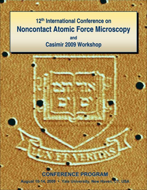
12 th International Conference on<br />
<strong>Noncontact</strong> <strong>Atomic</strong> <strong>Force</strong> <strong>Microscopy</strong><br />
and<br />
Casimir 2009 Workshop<br />
CONFERENCE PROGRAM<br />
August 10-14, 2009 � <strong>Yale</strong> University, New Haven, CT, USA
Institutional Sponsors<br />
<strong>Yale</strong> Center for Research<br />
on Interface Structures<br />
and Phenomena<br />
Past Conferences<br />
Osaka, Japan (1998)<br />
Pontresina, Switzerland (1999)<br />
Hamburg, Germany (2000)<br />
Kyoto, Japan (2001)<br />
Montreal, Canada (2002)<br />
Dingle, Ireland (2003)<br />
Seattle, USA (2004)<br />
Osnabrück, Germany (2005)<br />
Kobe, Japan (2006)<br />
Antalya, Turkey (2007)<br />
Madrid, Spain (2008)<br />
Forthcoming Conference<br />
Kanazawa, Japan (2010)<br />
Udo D. Schwarz<br />
Dept. <strong>of</strong> Mechanical <strong>Engineering</strong><br />
<strong>Yale</strong> University<br />
New Haven, CT 06515, USA<br />
udo.schwarz@yale.edu<br />
Cover Page: Banner <strong>of</strong> <strong>Yale</strong><br />
University (1.8 µm � 1.8 µm),<br />
written into a PMMA film by<br />
dynamic force microscopy.<br />
Image by M. Heyde &<br />
U. D. Schwarz<br />
Left: Harkness Tower on<br />
<strong>Yale</strong> Campus.<br />
• <strong>Yale</strong> <strong>School</strong> <strong>of</strong> <strong>Engineering</strong><br />
• Departments <strong>of</strong> Mechanical, Electrical,<br />
and Chemical <strong>Engineering</strong><br />
• Department <strong>of</strong> Physics<br />
Endorsed<br />
Topical<br />
Conference<br />
www.avs.org
Welcome<br />
Dear conference participant:<br />
Welcome to the 12th International Conference on Non-Contact <strong>Atomic</strong> <strong>Force</strong> <strong>Microscopy</strong><br />
(NC-AFM 2009), which is held on historic <strong>Yale</strong> University campus in New Haven, CT, USA.<br />
It continues a series <strong>of</strong> international conferences constituted 1998 in Osaka, Japan. Since<br />
then, the annual NC-AFM conferences have been established as the leading events for<br />
NC-AFM related topics. This year’s meeting has again attracted a large number <strong>of</strong><br />
participants (over 130 attendees from 17 countries), who are contributing 43 oral and 71<br />
poster presentations. 15 additional talks are provided by the Satellite Workshop on Casimir<br />
<strong>Force</strong>s and Their Measurement, and seven companies feature their newest products in an<br />
exhibition.<br />
Like in other years, the scientific program showcases the rapid development that NC-AFM<br />
enjoys. Various experimental improvements such as high-stability measurements<br />
performed at low temperatures, novel stiff self-sensing oscillators with atomically controlled<br />
tips that allow chemical identification and tunneling current collection, drift compensation by<br />
forward-feedbacking, atom tracking, and post-acquisition drift correction, and all-digital<br />
high-speed, low-noise electronics enable a new level <strong>of</strong> sophistication in imaging, analysis,<br />
and atom manipulation. Progress is particularly remarkable for high-resolution data<br />
acquisition in liquids, demonstrating that NC-AFM is leaving its ultrahigh vacuum niche.<br />
The main conference is complemented by a Satellite Workshop on Casimir <strong>Force</strong>s and<br />
Their Measurement (Casimir 2009). Designed to stimulate discussion between the Casimir<br />
and the NC-AFM communities, the Casimir 2009 workshop has been well received (87<br />
participants). Credit for initiating this event goes to Woo-Joong Kim, who was aided in its<br />
organization by Alex Sushkov and Steven K. Lamoreaux.<br />
Contributions by many key players were indispensable in realizing this conference, among<br />
them the ones by the members <strong>of</strong> the Local Organizing Committee (Eric I. Altman, Hong X.<br />
Tang, and Woo-Joong Kim) and by the team <strong>of</strong> the <strong>Yale</strong> Conference Service under the<br />
supervision <strong>of</strong> Susan Adler. Special thanks go to Mehmet Baykara for his help with various<br />
practical aspects such as the design <strong>of</strong> this abstract booklet. We were also fortunate to<br />
receive significant support from numerous <strong>Yale</strong> entities, whose generous financial<br />
assistance made this conference possible, from the European Science Foundation through<br />
its “New Trends and Applications <strong>of</strong> the Casimir Effect” program, and from the American<br />
Vacuum Society, which arranged for the publication <strong>of</strong> the conference proceedings. The<br />
complete list <strong>of</strong> institutional sponsors can be found opposite to this page; corporative<br />
sponsors and exhibitors are listed on page 9.<br />
We hope that you will enjoy the conference and have a wonderful time in New Haven.<br />
Udo D. Schwarz, Conference Chair<br />
1
2<br />
Contents<br />
Welcome 1<br />
Topics 3<br />
Committees 4<br />
General Information 6<br />
Local Maps 8<br />
Exhibitors 9<br />
Proceedings 10<br />
Conference Program 13<br />
Oral Presentations 28<br />
Poster Presentations 91<br />
Author Index 164<br />
List <strong>of</strong> Participants 169<br />
Advertisement 174
Topics<br />
• <strong>Atomic</strong> resolution imaging <strong>of</strong> surfaces, thin films, and molecular<br />
systems<br />
• Measuring tip-sample interaction potentials and mapping force fields<br />
• High-resolution imaging <strong>of</strong> clusters, biomolecules, and biological<br />
systems<br />
• High-resolution imaging and spectroscopy in liquid environments<br />
• Novel instrumentation and measurement techniques in dynamic AFM<br />
• Small amplitude measurements<br />
• Lateral force measurements using dynamic methods<br />
• <strong>Atomic</strong>- and molecular-scale manipulation<br />
• Theoretical analysis <strong>of</strong> contrast mechanisms; forces & tunnelling<br />
phenomena<br />
• Simulation <strong>of</strong> images and virtual AFM systems<br />
• Mechanisms for damping and energy dissipation<br />
• Amplitude modulation versus frequency modulation imaging<br />
• Measuring nanoscale charges, work functions, and magnetic<br />
properties<br />
• Characterization and modification <strong>of</strong> force microscopy tips at the<br />
atomic scale<br />
3
Committees<br />
Conference Chairman<br />
Udo Schwarz <strong>Yale</strong> University (USA)<br />
Local Organizing Committee<br />
Eric I. Altman <strong>Yale</strong> University (USA)<br />
Hong X. Tang <strong>Yale</strong> University (USA)<br />
Woo-Joong Kim <strong>Yale</strong> University (USA)<br />
Satellite Workshop Organization<br />
Woo-Joong Kim <strong>Yale</strong> University (USA)<br />
Udo Schwarz <strong>Yale</strong> University (USA)<br />
Alex Sushkov <strong>Yale</strong> University (USA)<br />
Steven K. Lamoreaux <strong>Yale</strong> University (USA)<br />
International Steering Committee<br />
Franz Giessibl University <strong>of</strong> Regensburg (Germany)<br />
Peter Grütter McGill University (Canada)<br />
Ernst Meyer University <strong>of</strong> Basel (Switzerland)<br />
Seizo Morita Osaka University (Japan)<br />
Hiroshi Onishi Kobe University (Japan)<br />
Ahmet Oral Sabanci University (Turkey)<br />
Rubén Peréz Universidad Autonoma de Madrid (Spain)<br />
Michael Reichling University <strong>of</strong> Osnabrück (Germany)<br />
Alexander Schwarz University <strong>of</strong> Hamburg (Germany)<br />
Udo Schwarz <strong>Yale</strong> University (USA)<br />
Alexander Shluger University College London (UK)<br />
4
Committees<br />
Program Committee<br />
Jaime Colchero Universidad de Murcia (Spain)<br />
Oscar Custance National Institute for Material Science (Japan)<br />
Takeshi Fukuma Kanazawa University (Japan)<br />
Hendrik Hölscher Karlsruhe Research Laboratory (Germany)<br />
Sascha Sadewasser Helmholtz Institute Berlin (Germany)<br />
André Schirmeisen University <strong>of</strong> Münster (Germany)<br />
Santiago Solares University <strong>of</strong> Maryland (USA)<br />
Yasuhiro Sugawara Osaka University (Japan)<br />
Masaru Tsukada Waseda University (Japan)<br />
Hir<strong>of</strong>umi Yamada Kyoto University (Japan)<br />
Conference Proceedings Editors<br />
Hendrik Hölscher Karlsruhe Research Laboratory (Germany)<br />
Udo D. Schwarz <strong>Yale</strong> University (USA)<br />
Conference Organization<br />
Tara Schule, Joanne Dupee, Roberta Hudson, and Susan Adler, <strong>Yale</strong> Conference<br />
Services<br />
5
General Information<br />
Conference Venue:<br />
Talks will be held in Davies Auditorium in the basement <strong>of</strong> <strong>Yale</strong> University’s Becton Center,<br />
15 Prospect Street, New Haven, CT 06511 (see the maps page 8 for the exact location).<br />
For easiest access, follow the signs around the building to the lower courtyard located<br />
between Becton Center and the rear building (Dunham Laboratory, 10 Hillhouse Avenue).<br />
There, you will find the main entrance to the conference area, which is indicated by the red<br />
arrow in the satellite picture. For the auditorium, please turn left after entering the doors. In<br />
contrast, turning right twice will lead you to the J. Robert Mann Jr. <strong>Engineering</strong> Student<br />
Center, where c<strong>of</strong>fee breaks and parts <strong>of</strong> the exhibition are taking place. Poster sessions<br />
and luncheons will be held in Commons Hall at the corner <strong>of</strong> Grove and College Streets<br />
(the building with the dome opposite Becton Center). Please keep in mind that smoking is<br />
not allowed in any <strong>Yale</strong> University building, including Davies Auditorium, the Mann Student<br />
Center, and Commons Hall.<br />
Registration:<br />
The registration desk in the foyer <strong>of</strong> Davies Auditorium (see above) will be staffed 07:45-<br />
18:00 (Monday), 08:00-12:00 (Tuesday), and 08:30-09:00 (Wednesday through Friday).<br />
Welcome Party:<br />
We invite all conference participants to a casual welcome party with reception and dinner<br />
(barbeque) on Monday, August 10, 2009, between 18:30 and 20:30. The exact location will<br />
be announced ahead <strong>of</strong> time via email and on the web.<br />
Conference Banquet:<br />
Conference banquet will be held on Thursday, Aug. 13 th , 2009, 18:30-22:00 at Sterling<br />
Memorial Library (SML) on <strong>Yale</strong> campus. Please see the maps on page 8 for the location <strong>of</strong><br />
SML.<br />
6
General Information (cont.)<br />
Oral Presentations:<br />
Oral presentations will be scheduled for 20 minutes each including a 5-minute discussion<br />
for sessions during the NC-AFM conference (August 11-14). For the specialized Casimir<br />
workshop sessions on August 10, talks will be 25 minutes each. An LCD projector is<br />
available in the conference room, but all speakers are required to bring their own laptops.<br />
Poster Presentations:<br />
Two Poster sessions will be held during the conference on Tuesday, August 11, and<br />
Wednesday, August 12, 2009. The available size for posters will be 1.2 m x 1.2 m. Pins for<br />
mounting the poster on the board will be provided.<br />
Internet Access:<br />
Wireless internet access will be available in Davies Auditorium and the exhibition areas.<br />
Detailed instructions for connecting to the internet will be distributed with your conference<br />
material. Also, a number <strong>of</strong> desktop computers will be available in the exhibition area and a<br />
nearby computer cluster room. A guest login ID and a personal password, which allows you<br />
to connect to the internet from these computers, will be handed to each participant at the<br />
registration desk.<br />
7
Local Maps<br />
8
Exhibitors<br />
9
Proceedings<br />
Both NC-AFM Conference and Casimir Workshop participants are invited to contribute an<br />
article to the conference proceedings, which will be published in the Journal <strong>of</strong> Vacuum<br />
Science and Technology B (JVST B). Publishing your work in the conference proceedings<br />
represents an excellent opportunity to promote your work, as NC-AFM proceedings have in<br />
the past always been highly visible and widely cited. This is in particular the case as every<br />
conference participant (main conference AND Casimir Workshop) will receive a bound<br />
complementary copy <strong>of</strong> the proceedings via mail.<br />
The proceedings will be edited by Hendrik Hölscher, Karlsruhe Research Laboratory,<br />
Germany, and Udo D. Schwarz, <strong>Yale</strong> University. Submission deadline is October 16,<br />
2009, but please contact us at your earliest convenience to let us know about your plans to<br />
submit a contribution so that we can plan ahead. Publication <strong>of</strong> the proceedings is<br />
scheduled for the May/June issue <strong>of</strong> JVST B in 2010.<br />
Instructions for preparing manuscripts for the proceedings <strong>of</strong> the NC-AFM 2009<br />
Conference:<br />
1. Submission: Papers will be reviewed according to criteria set by the JVST and must<br />
meet JVST standards for both technical content and written English. All manuscripts<br />
for the proceedings must be submitted as a PDF file along with a cover letter<br />
containing your complete address to the guest editor via email<br />
(Hendrik.Hoelscher@imt.fzk.de).<br />
2. Program number: It is important that the submitted manuscript has the program<br />
number <strong>of</strong> your contribution to the NC-AFM conference or the satellite conference<br />
entered in the top-right corner <strong>of</strong> the title page.<br />
10
Proceedings (cont.)<br />
3. Length: Papers can contain up to a nominal total <strong>of</strong> 20-25 pages <strong>of</strong> double-spaced<br />
text, tables, figures, references, abstract, etc. if the submitted paper is longer than<br />
25 pages, the final decision on acceptance for publication will be made by the JVST<br />
editors based on the recommendations <strong>of</strong> the reviewers.<br />
4. Format: The text should be double-spaced; the font recommended by JVST is<br />
Times New Roman 12pt. Pages should have one-inch margins on all sides.<br />
5. Figures and Tables: Each figure and table should be displayed on a separate<br />
page. Table and figure captions should be listed on a separate page and NOT below<br />
the table or figure; only the figure/table number must appear with the figure/table.<br />
6. Footnotes: Authors may include their e-mail addresses along with all other footnotes<br />
in the following format: Electronic mail: smith@yale.edu<br />
7. Costs: JVST publishes articles authored by members <strong>of</strong> the American Vacuum<br />
Society (AVS) free <strong>of</strong> charge. Therefore, let us know when submitting whether any <strong>of</strong><br />
the authors is presently AVS member. For submissions where no author is AVS<br />
member, we will provide a complementary 1-year membership for the paper's<br />
corresponding author paid for form conference funds. As a result, there will be no<br />
page charges or other costs for your submission.<br />
8. Color: Your figures can appear online in color for free. To take advantage <strong>of</strong> this<br />
<strong>of</strong>fer, you will need to send the electronic file(s) <strong>of</strong> your figure(s) within 24 hours <strong>of</strong><br />
receiving your acceptance email from JVST directly to the publisher (the American<br />
Institute <strong>of</strong> Physics, AIP). Please do not send anything until you receive notice the<br />
paper is accepted and has a 9 digit AIP number. Sending color figures in the pdf file<br />
11
Proceedings (cont.)<br />
used for the review process does not allow for color reproduction (either online or<br />
print) at the publishing stage. Only sending AIP the files directly will enable this. A<br />
“Publisher’s Announcements” email with more details will be sent to you once your<br />
paper has been accepted.<br />
9. Materials Index Entries: If applicable, please provide us with at least three material<br />
terms, which should indicate what materials (i.e., chemical species) are discussed in<br />
the article. These terms are needed as entries for the JVST Materials Index.<br />
For more details, please refer to:<br />
JVST author instructions: www.avs.org/literature.information.aspx<br />
JVST Word template: www.avs.org/pdf/JVST/eC.doc<br />
Instructions for this template: www.avs.org/pdf/JVST/eCEinstructions.pdf<br />
Manuscript deadline: October 16, 2009<br />
Please submit your manuscript as PDF together with a cover letter containing your<br />
complete address and information whether or not one <strong>of</strong> the authors is presently AVS<br />
member via email to guest editor Dr. Hendrik Hölscher at Hendrik.Hoelscher@imt.fzk.de<br />
12
Conference<br />
Program<br />
13
NC-AFM 2009<br />
Sessions<br />
Monday<br />
August 10<br />
• Liquids I<br />
Tuesday 9:20-10:40<br />
• <strong>Force</strong> Spectroscopy I<br />
Tuesday 11:20-12:40<br />
• Electronic, photonic, & Casimir forces<br />
Tuesday 14:30-15:50<br />
• Oxides<br />
Wednesday 9:00-10:40<br />
• Carbon-based materials<br />
Wednesday 11:20-12:40<br />
Tuesday<br />
August 11<br />
14<br />
Wednesday<br />
August 12<br />
• Molecules on insulators<br />
Wednesday 14:30-15:50<br />
• <strong>Force</strong> spectroscopy II<br />
Thursday 9:00-10:40<br />
• <strong>Force</strong>s & charges<br />
Thursday 11:20-13:00<br />
• Method development<br />
Friday 9:00-10:40<br />
• Liquids II<br />
Friday 11:20-12:40<br />
Thursday<br />
August 13<br />
Friday<br />
August 14<br />
8:30 Registration Registration Registration Registration<br />
9:00 Opening Remarks M. Heyde A. Campbellova Y. Naitoh<br />
9:20 T. Fukuma A. Yurtsever F. J. Giessibl S. Torbrügge<br />
9:40 H. Asakawa R. Pérez G. Langewisch Y. Hosokawa<br />
10:00 N. Oyabu R. Bechstein A. Barat<strong>of</strong>f E. Tsunemi<br />
10:20 M. Tsukada S. Sadewasser S. Kawai U. Zerweck<br />
10:40 C<strong>of</strong>fee Break C<strong>of</strong>fee Break C<strong>of</strong>fee Break C<strong>of</strong>fee Break<br />
11:20 D. Ebeling U. D. Schwarz A. Sweetman S. Nishida<br />
11:40 A. Schirmeisen P. Jelínek L. Gross S. Ido<br />
12:00 Y. Sugimoto M. Ashino Y. Miyahara E. T. Herruzo<br />
12:20 Y. Sugawara P. Pou T. Trevethan K. Fukui<br />
12:40 A. Bettac Closing Remarks<br />
13:00<br />
Lunch<br />
110 min.<br />
(12:40-14:30)<br />
Lunch<br />
110 min.<br />
(12:40-14:30)<br />
14:30<br />
A. Parsegian<br />
A. Kühnle<br />
14:50<br />
(invited)<br />
A. Schwarz<br />
15:10 Th. Glatzel Ch. Loppacher<br />
15:30 H. Hölscher C. J. Gómez<br />
15:50<br />
|<br />
18:00<br />
C<br />
A<br />
S<br />
I<br />
M<br />
I<br />
R<br />
W<br />
O<br />
R<br />
K<br />
S<br />
H<br />
O<br />
P<br />
18:30-20:30<br />
Welcome<br />
Reception/Dinner<br />
Poster Session I Poster Session II<br />
Lunch<br />
90 min.<br />
(13:00-14:30)<br />
18:30-22:00<br />
Conference<br />
Banquet
Program Summary <strong>of</strong> the NC-AFM 2009 Satellite Workshop on<br />
Casimir <strong>Force</strong>s and Their Measurement<br />
Monday sessions only; Tuesday sessions are joint with the NC-AFM Conference (see the main<br />
conference program for listing). Note in particular that the Casimir workshop’s second invited talk,<br />
given by Adrian Parsegian (NIH, USA), will take place Tuesday 14:30-15:10.<br />
Monday, August 10<br />
7:45 Registration<br />
8:50 Opening Remarks<br />
9:00 Rudi Porgornik (University <strong>of</strong> Ljubljana, Slovenia), invited<br />
9:30 Noah Graham (Middlebury College, USA)<br />
9:55 Kimball Milton (University Oklahoma, USA)<br />
10:20<br />
C<strong>of</strong>fee Break<br />
10:50 Raul Esquivel-Sirvent (Universidad Nacional Autónoma, Mexico)<br />
11:15 Diego Dalvit (Los Alamos National Laboratory, USA)<br />
11:40 Rick Rajter (MIT, USA)<br />
12:05 Maarten de Boer (Sandia National Laboratory, USA)<br />
12:30<br />
Lunch (12:30-14:30)<br />
14:30 Hong Tang (<strong>Yale</strong> University, USA)<br />
14:55 Alessandro Siria (CNRS, France)<br />
15:20 Arvind Narayanaswamy (Columbia University, USA)<br />
15:45<br />
C<strong>of</strong>fee Break<br />
16:15 Sven de Man (VU University Amsterdam, Netherlands)<br />
16:40 Gauthier Torricelli (University <strong>of</strong> Leicester, UK)<br />
17:05 Ho Bun Chan (University <strong>of</strong> Florida, USA)<br />
17:30 Peter van Zwol (University <strong>of</strong> Groningen, Netherlands)<br />
17:55 Woo-Joong Kim (<strong>Yale</strong> University, USA)<br />
18:30-20:30<br />
Welcome Reception with Dinner<br />
15
Monday, August 10<br />
Satellite Workshop on Casimir <strong>Force</strong>s and<br />
Their Measurement<br />
8:50 Opening Remarks<br />
Session I Chair: W.-J. Kim<br />
9:00 Non-retarded and retarded interactions between dielectric cylinders<br />
Rudi Podgornik<br />
9:30 Casimir <strong>Force</strong>s from Scattering Theory<br />
Noah Graham<br />
9:55 Multiple Scattering Casimir <strong>Force</strong> Calculations between Layered and Corrugated Materials<br />
Kimball Milton<br />
10:20 C<strong>of</strong>fee Break<br />
Session II Chair: R. Podgornik<br />
10:50 Drude corrections to Casimir force calculations in liquids<br />
Raul Esquivel-Sirvent<br />
11:15 Dispersive Casimir interactions between atoms and surfaces<br />
Diego Dalvit<br />
11:40 Van der Waals with a twist: how nanotube chirality impacts interaction strength<br />
Rick Rajter<br />
12:05 Using Casimir and capillary forces to model adhesion <strong>of</strong> MEMS cantilevers<br />
Maarten de Boer<br />
12:30 Lunch Break<br />
Session III Chair: A. Parsegian<br />
14:30 Measuring “Virtual Photon” <strong>Force</strong>s with “Real Photon” <strong>Force</strong>s<br />
Hong Tang<br />
14:55 Near-field radiative heat transfer<br />
Alessandro Siria<br />
15:20 Near-field radiative transfer measurements and implications for Casimir force<br />
measurements<br />
Arvind Narayanaswamy<br />
15:45 C<strong>of</strong>fee Break<br />
16
Monday, August 10<br />
Satellite Workshop on Casimir <strong>Force</strong>s and Their Measurement (cont.)<br />
Session IV<br />
17<br />
Chair: D. Dalvit<br />
16:15 Tricks and facts in a high precision measurement <strong>of</strong> the Casimir force with transparent<br />
conductors<br />
Sven de Man<br />
16:40 Measurements <strong>of</strong> the Casimir force gradient by AFM for Different Materials<br />
Gauthier Torricelli<br />
17:05 Measuring the topological dependence <strong>of</strong> the Casimir force on nanostructured silicon<br />
surfaces<br />
Ho Bun Chan<br />
17:30 Short range Casimir force measurements under ambient conditions and liquid<br />
environments<br />
Peter van Zwol<br />
17:55 Contact potential difference in a Casimir force measurement: How do we deal with it?<br />
Woo-Joong Kim<br />
Welcome Reception with Dinner (18:30-20:30)
Tuesday, August 11<br />
9:00 Opening Remarks<br />
Liquids I<br />
9:20 3D Scanning <strong>Force</strong> <strong>Microscopy</strong> at Solid/Liquid Interface<br />
T. Fukuma, Y. Ueda<br />
18<br />
Chair: H. Hölscher<br />
9:40 Anisotropic Hydration <strong>of</strong> Biological Molecules Visualized by Three-Dimensional Scanning<br />
<strong>Force</strong> <strong>Microscopy</strong><br />
H. Asakawa,Y. Ueda, T. Fukuma<br />
10:00 Experimental and Theoretical Studies on 3D Hydration Structures on Muscovite Mica<br />
Surfaces in Aqueos Solution<br />
N. Oyabu, K. Kimura, S. Ido, K. Suzuki, K. Kobayashi, T. Imai, H. Yamada<br />
10:20 Theory <strong>of</strong> Tip-Sample Interaction <strong>Force</strong> Mediated by Water<br />
M. Tsukada, M.Harada, K.Tagami<br />
10:40 C<strong>of</strong>fee Break<br />
<strong>Force</strong> Spectroscopy I<br />
11:20 Dynamic <strong>Force</strong> Spectroscopy <strong>of</strong> Single Chain-like Molecules<br />
D. Ebeling, H. Fuchs, F. Oesterhelt, H. Hölscher<br />
11:40 Spatial force fields above a single atom defect<br />
A. Schirmeisen, D. Weiner<br />
12:00 Simultaneous measurement <strong>of</strong> force and tunneling current<br />
D. Sawada, Y. Sugimoto, K.-I. Morita, M. Abe, S. Morita<br />
12:20 Atom Manipulation on Cu(110)-O Surface with LT-AFM<br />
Y. Sugawara, Y. Kinoshita, Y. J. Li, Y. Naitoh, M. Kageshima<br />
12:40 Lunch Break<br />
Chair: F. J. Giessibl<br />
Electronic, Photonic, & Casimir <strong>Force</strong>s Chair: S. Morita<br />
14:30 Water, Ions, Membranes, Real Metals, Finite Temperature: Is there ever a pure Casimir<br />
force? (Invited)<br />
Adrian Parsegian<br />
15:10 Short and medium range electrostatic forces analyzed by Kelvin probe force microscopy<br />
Th. Glatzel, S. Kawai, S. Koch, A. Barat<strong>of</strong>f, E. Meyer<br />
15:30 The Effective Quality Factor in Dynamic <strong>Force</strong> Microscopes with Fabry-Perot<br />
Interferometer Detection<br />
H. Hölscher, P. Milde, U. Zerweck, L. M. Eng, R. H<strong>of</strong>fmann<br />
Poster Session I (15:50 – 18:00)<br />
Chair: A. Oral
Wednesday, August 12<br />
Oxides Chair: A. Schwarz<br />
9:00 Imaging Single Atoms on Oxide Surfaces – Gold on Alumina/NiAl(110)<br />
M. Heyde, G. H. Simon, Th. König, H.-J. Freund<br />
9:20 Site-specific force spectroscopy on TiO2 (110) surface at low-temperature<br />
A. Yurtsever, A. Pratama, Y. Sugimoto, M. Abe, S. Morita<br />
9:40 Character <strong>of</strong> the short-range interaction between a silicon based tip and the TiO2(110)<br />
surface: a DFT study<br />
C. Gozalez, P. Jelínek, R. Pérez<br />
10:00 True atomic resolution imaging on an application-oriented system: Understanding<br />
photocatalytic reactivity <strong>of</strong> transition-metal doped TiO2<br />
R. Bechstein, M. Kitta, J. Schütte, H. Onishi, A. Kühnle<br />
10:20 Local surface photovoltage spectroscopy <strong>of</strong> molecular clusters using Kelvin probe force<br />
microscopy<br />
S. Sadewasser, M. Ch. Lux-Steiner<br />
10:40 C<strong>of</strong>fee Break<br />
Carbon-based Materials Chair: M. Reichling<br />
11:20 Why is Graphite so Slippery? Gathering Clues from Three-Dimensional Lateral <strong>Force</strong>s<br />
Measurements<br />
U. D. Schwarz, M. Z. Baykara, T. C. Schwendemann, B. J. Albers, N. Pilet, E. I. Altman<br />
11:40 Theoretical DFT simulations <strong>of</strong> the STM/AFM atomic scale imaging on graphite<br />
V. Rozsíval, M. Ondráček, P. Jelínek<br />
12:00 <strong>Atomic</strong>-Resolution Damping <strong>Force</strong> Spectroscopy on Nanotube Peapods with Different<br />
Tube Diameters<br />
M. Ashino, R. Wiesendanger, A. N. Khlobystov, S. Berber, D. Tománek<br />
12:20 Theoretical study <strong>of</strong> the forces and atomic configurations <strong>of</strong> NC-AFM experiments on lowdimension<br />
carbon materials<br />
P. Pou, R. Perez<br />
12:40 Lunch Break<br />
Molecules on Insulators Chair: R. Perez<br />
14:30 Anchoring highly polar molecules onto an ionic crystal<br />
J. Schütte, R. Bechstein, M. Rohlfing, M. Reichling, A. Kühnle<br />
14:50 Steering the formation <strong>of</strong> molecular nanowires and compact nanocrystallites on NaCl(001)<br />
S. Fremy, A. Schwarz, K. Laemmle, R. Wiesendanger, M. Prosenc<br />
15:10 2-Dimensional growth <strong>of</strong> phenylenediboronic acid assisted by H-bonding<br />
R. Pawlak, L. Nony, F. Bocquet, M. Sassi, V. Oison, J.-M. Debierre, Ch. Loppacher, L.<br />
Porte<br />
15:30 Molecular scale dissipation in oligothiophene monolayers measured by dynamic force<br />
microscopy<br />
C. J. Gómez, N. F. Martínez, W. Kamiński, C. Albonetti, F. Biscarini, R. Perez, R. Garcia<br />
Poster Session II (15:50 – 18:00) Chair: Y. Sugawara<br />
19
Thursday, August 13<br />
<strong>Force</strong> Spectroscopy II<br />
20<br />
Chair: P. Grütter<br />
9:00 Dependence <strong>of</strong> the atomic scale image <strong>of</strong> a Si adatom on the tip apex termination: a DFT<br />
study<br />
A. Campbellova, P. Pou , R. Pérez, P. Klapetek, P. Jelínek<br />
9:20 AFM probe tips with a small front atom<br />
T. H<strong>of</strong>mann, J. Welker, M. Ternes, C. P. Lutz, A. J. Heinrich, F. J. Giessibl<br />
9:40 Intramolecular features <strong>of</strong> organic molecules characterized by force field spectroscopy:<br />
The case <strong>of</strong> PTCDA on Cu and Ag<br />
G. Langewisch, D.-A. Braun, D. Weiner, B. Such, H. Fuchs, A. Schirmeisen<br />
10:00 Analysis <strong>of</strong> bimodal and higher mode small-amplitude near-contact AFM and energy<br />
dissipation<br />
S. Kawai, A. Barat<strong>of</strong>f, Th. Glatzel, S. Koch, B. Such, E. Meyer<br />
10:20 Adhesion-induced energy dissipation and atom-tracked tip changes<br />
S. Kawai, Th. Glatzel, S. Koch, B. Such, A. Barat<strong>of</strong>f, E. Meyer<br />
10:40 C<strong>of</strong>fee Break<br />
<strong>Force</strong>s & Charges<br />
Chair: H. Onishi<br />
11:20 Combined Qplus-AFM and STM imaging <strong>of</strong> the Si(100) surface: Activating the c(4x2) to<br />
p(2x1) transition with subnanometre oscillation amplitudes<br />
A. Sweetman, S. Gangopadhyay, R. Danza, P. Moriarty<br />
11:40 Measuring <strong>Atomic</strong> Charge States by nc-AFM<br />
L. Gross, F. Mohn, P. Liljeroth, J. Repp, F. J. Giessibl, G. Meyer<br />
12:00 Mechanism <strong>of</strong> Dissipative Interaction by Tunneling Single-Electrons<br />
Y. Miyahara, L. Cockins, S. D. Bennett, A. A. Clerk, S. A. Studenikin, P. Poole, A.<br />
Sachrajda, P. Grütter<br />
12:20 Controlling electron transfer processes on insulating surfaces with the NC-AFM<br />
Th. Trevethan, A. Shluger<br />
12:40 NC-AFM imaging with atomic resolution in a temperature range between 5 K and 1083 K<br />
A. Bettac, A. Feltz<br />
13:00 Lunch Break<br />
Guided <strong>Yale</strong> Campus Walking Tour (16:00-17:30)<br />
Conference Banquet (18:30 – 22:00)
Friday, August 14<br />
Method Development Chair: A. Schirmeisen<br />
9:00 <strong>Atomic</strong> scale elasticity mapping <strong>of</strong> Ge(001) surface by multifrequency FM-AFM<br />
Y. Naitoh, Z. Ma, Y. Li, M. Kageshima, Y. Sugawara<br />
9:20 Small amplitude atomic resolution NC-AFM imaging and force spectroscopy experiments<br />
using a stiff piezoelectric force sensor<br />
S. Torbrügge, J. Rychen, O. Schaff<br />
9:40 Determination <strong>of</strong> the Optimum Spring Constant and Oscillation Amplitude for<br />
<strong>Atomic</strong>/Molecular-Resolution FM-AFM<br />
Y. Hosokawa, K. Kobayashi, H. Yamada, K. Matsushige<br />
10:00 Visualization <strong>of</strong> Anisotropic Conductance in Polydiacetylene Crystal by Two-probe FM-<br />
AFM/KFM<br />
E. Tsunemi, K. Kobayashi, K. Matsushige, H. Yamada<br />
10:20 Scattering Scanning Near-Field Optical <strong>Microscopy</strong> performed by NC-AFM<br />
U. Zerweck, S. C. Schneider, M. T. Wenzel, H.-G. von Ribbeck, S. Grafström, R. Jacob, S.<br />
Winnerl, M. Helm, L. M. Eng<br />
10:40 C<strong>of</strong>fee Break<br />
Liquids II Chair: T. Fukuma<br />
11:20 <strong>Atomic</strong> resolution dynamic lateral force microscopy in liquid<br />
S. Nishida, D. Kobayashi, N. Okabe, H. Kawakatsu<br />
11:40 Molecular-scale Investigations <strong>of</strong> Biomolecules in Liquids by FM-AFM<br />
S. Ido, N. Oyabu, K. Kobayashi, Y. Hirata, M. Tsukada, K. Matsushige, H. Yamada<br />
12:00 Bimodal AFM imaging <strong>of</strong> antibodies and chaperonins in liquids<br />
E. T. Herruzo, C. Dietz, J. R. Lozano, R.Garcia<br />
12:20 Redox-state Dependent Reversible Change <strong>of</strong> Molecular Ensembles in Water Solution by<br />
Electrochemical FM-AFM<br />
K.-I. Umeda, Y. Yokota, K.-I. Fukui<br />
12:40 Closing Remarks<br />
21
POSTER Session I (Tuesday)<br />
<strong>Force</strong> Spectroscopy<br />
P.I-01 <strong>Force</strong> and Tunneling Current Measurements on the Semiconductor Surface<br />
D. Sawada, Y. Sugimoto, K.-I. Morita, M. Abe, S. Morita<br />
P.I-02 <strong>Force</strong> Map <strong>of</strong> <strong>Atomic</strong> <strong>Force</strong> <strong>Microscopy</strong> on Si(111)-(5x5)-DAS Surface<br />
A. Masago, M. Tsukada<br />
22<br />
Chair: A. Oral<br />
P.I-03 From non-contact to atomic scale contact between a Si tip and a Si surface analyzed using<br />
an nc-AFM and nc-AFS based instrument<br />
T. Arai, K. Kiyohara, T. Sato, S. Kushida, M. Tomitori<br />
P.I-04 Improved atomic-scale contrast via bimodal dynamic force microscopy<br />
S. Kawai, Th. Glatzel, S. Koch, B. Such, A. Barat<strong>of</strong>f, E. Meyer<br />
P.I-05 Static cantilever deflection in dynamic force microscopy<br />
S. Kawai, Th. Glatzel, S. Koch, B. Such, A. Barat<strong>of</strong>f, E. Meyer<br />
P.I-06 Resonance frequency shift due to tip-sample interaction in the thermal oscillations regime<br />
G. Malegori, G. Ferrini<br />
P.I-07 Influence <strong>of</strong> thermal noise on measurements <strong>of</strong> chemical bonds in UHV-AFM<br />
P. M. H<strong>of</strong>fmann<br />
P.I-08 <strong>Atomic</strong> force microscope cantilever resonance frequency shift based thermal metrology<br />
A. Narayanaswamy, C. Canetta, N. Gu<br />
Kelvin Probe <strong>Microscopy</strong><br />
P.I-09 Contact potential difference on the atomic-scale probed by Kelvin Probe <strong>Force</strong> <strong>Microscopy</strong>:<br />
an imaging scenario<br />
L. Nony, A. Foster, F. Bocquet, Ch. Loppacher<br />
P.I-10 Self-assembled Boronitride Nanomesh on Rh(111) Investigated by Means <strong>of</strong> Kelvin Probe<br />
<strong>Force</strong> <strong>Microscopy</strong><br />
S. Koch, M. Langer, J. Lobo-Checa, Th. Brugger, S. Kawai, B. Such, E. Meyer, Th. Glatzel<br />
P.I-11 Kelvin probe force microscopy in application to organic thin films: frequency modulation,<br />
amplitude modulation, and hover mode KPFM<br />
B. Moores, F. Hane, L. M. Eng, Z. Leonenko<br />
P.I-12 Resolution enhanced multifrequency electrostatic force microscopy under ambient<br />
conditions<br />
X. D. Ding, J. B. Xu, J. X. Zhang<br />
P.I-13 Deconvolution and Tip Geometry Effects in <strong>Atomic</strong>- and Nanoscale Kelvin probe <strong>Force</strong><br />
<strong>Microscopy</strong><br />
G. Elias, Y. Rosenwaks, A. Boag, E. Meyer, Th. Glatzel<br />
P.I-14 Kelvin <strong>Force</strong> <strong>Microscopy</strong> Dynamic Behavior and Noise Propagation<br />
H. Diesinger, D. Deresmes, J.-P. Nys, Th. Mélin<br />
P.I-15 Charge transfer from doped silicon nanocrystals<br />
Ł. Borowik, Th. Nguyen-Tran, P. Roca i Cabarrocas, K. Kusiaku, D. Theron, H. Diesinger,<br />
D. Deremes, Th. Mélin
Poster Session I cont. (Tuesday)<br />
Instrumentation<br />
P.I-16 Open source scanning probe microscopy control and data analysis s<strong>of</strong>tware package<br />
Gxsm<br />
P. Zahl<br />
P.I-17 2 nd generation Dynamic Nanostencil AFM/DFM/STM for in-situ (UHV) resistless patterning<br />
<strong>of</strong> nanostructures<br />
P. Zahl, P. Sutter<br />
P.I-18 Design <strong>of</strong> a Variable Temperature Variable Magnetic Field <strong>Noncontact</strong> Scanning <strong>Force</strong><br />
Microscope for the Characterization <strong>of</strong> Nanoscale Electronic and Magnetic Phenomena<br />
P. Staffier, M. Liebmann, J. Falter, N. Pilet, Ch. Ahn, U. D. Schwarz<br />
P.I-19 An Active Q Control System in Scanning <strong>Force</strong> <strong>Microscopy</strong><br />
J. Kim, M. Zech, J. E. H<strong>of</strong>fman<br />
P.I-20 Besocke style quartz tuning fork FM-AFM/STM for use in UHV and low temperatures<br />
S. M. Huston, R. T. Port, K. M. Andrews, Th. P. Pearl<br />
P.I-21 Design <strong>of</strong> a Low Temperature <strong>Noncontact</strong> <strong>Atomic</strong> <strong>Force</strong> Microscope Combined with a Field<br />
Ion Microscope<br />
J. Falter, D.-A. Braun, H. Hölscher, U. D. Schwarz, A. Schirmeisen, H. Fuchs<br />
P.I-22 A homebuilt low-temperature STM / tuning fork AFM combination<br />
M. Lange, J. Schaffert, N. Wintjes, R. Möller<br />
P.I-23 Development <strong>of</strong> quartz force sensors for noncontact atomic force microscopy/spectroscopy<br />
K. Hori, T. Arai, M. Tomitori<br />
P.I-24 High-Speed Frequency Modulation <strong>Atomic</strong> <strong>Force</strong> <strong>Microscopy</strong> using Wideband Digital<br />
Phase-Locked Loop Detector<br />
T. Fukuma, Y. Mitan<br />
Method Development<br />
P.I-25 Recent Advances in Multi-Spectral <strong>Atomic</strong> <strong>Force</strong> <strong>Microscopy</strong><br />
S. Jesse, N. Balke, P. Maksymovych, O. Ovchinnikov, A.P. Baddorf, S.V. Kalinin<br />
P.I-26 Deciphering Nanoscale Interactions: Artificial Neural Networks and Scanning Probe<br />
<strong>Microscopy</strong><br />
M. Nikiforov, S. Jesse, O. Ovchinnikov, S. V. Kalinin<br />
P.I-27 NC-AFM study <strong>of</strong> a cleaved InAs (110) surface using modified Si probes under ambient<br />
atmospheric pressure<br />
Y. Jeong, M. Hirade, R. Kokawa, H. Yamada, K. Kobayashi, N. Oyabu, H. Yamatani, T.<br />
Arai, A. Sasahara, M. Tomitori<br />
P.I-28 Dual-Frequency-Modulation AFM Spectroscopy<br />
G. Chawla, C. A. Wright, S. D. Solares<br />
P.I-29 Theory <strong>of</strong> Multifrequency Method in FM-AFM<br />
Z. Ma, Y. Naitoh, Y. Li, M. Kageshima, Y. Sugawara<br />
P.I-30 Internal Resonances and Spatio-Temporal Instabilities in Nonlinear Multi-mode NC-AFM<br />
Dynamics<br />
O. Gottlieb, S. Hornstein, W. Wu, A. Shavit<br />
23
Poster Session I cont. (Tuesday)<br />
P.I-31 Frequency Noise in Frequency Modulation <strong>Atomic</strong> <strong>Force</strong> <strong>Microscopy</strong><br />
K. Kobayashi, H. Yamada, K. Matsushige<br />
P.I-32 Relation between lateral forces and dissipation in FM-AFM<br />
M. Klocke, D. E. Wolf<br />
P.I-33 Experimental Study <strong>of</strong> Dissipation Mechanisms in AFM Cantilevers<br />
F. Zypman<br />
Nanolithography<br />
P.I-34 Ultrasonic Nanolithography on Hard Substrates<br />
M. T. Cuberes<br />
P.I-35 Silicon nanowire transistors with a channel width <strong>of</strong> 4 nm fabricated by atomic force<br />
microscope nanolithography<br />
J. Martinez, R. V. Martinez, R. Garcia<br />
P.I-36 Contacting self-ordered molecular wires by nanostencil lithography<br />
L. Gross, R. R. Schlittler, G. Meyer, Th. Glatzel, S. Kawai, S. Koch, E. Meyer<br />
24
POSTER Session II (Wednesday)<br />
Molecules<br />
25<br />
Chair: Y. Sugawara<br />
P.II-01 Molecular Structures <strong>of</strong> Organic Single Crystals Investigated by Frequency Modulation<br />
<strong>Atomic</strong> <strong>Force</strong> Microscopes<br />
T. Minato, H. Aoki, T. Wagner, K. Itaya<br />
P.II-02 Imaging <strong>of</strong> aromatic molecules by tuning-fork based LT-NC-AFM<br />
B. Such, Th. Glatzel, S. Kawai, S. Koch, A. Barat<strong>of</strong>f, E. Meyer, C. H. M. Amijs, P. de<br />
Mendoza, A. M. Echavarren<br />
P.II-03 One and Two Dimensional Structure <strong>of</strong> Water on Cu(110) and O/Cu(110)-(2x1) Surface<br />
B. Y. Choi, Y. Shi, T. Duden, M. Salmeron<br />
P.II-04 Dynamical simulations <strong>of</strong> truxene molecules adsorbed on the KBr (001) surface<br />
T. Trevethan, A. Shluger<br />
P.II-05 Temperature-dependent growth <strong>of</strong> C60 on CaF2(111)<br />
F. Loske, P. Maaß, J. Schütte, A. Kühnle<br />
P.II-06 Creating 1D nanostructures: Heptahelicene-carboxylic acid on Calcite<br />
P. Rahe, M. Nimmrich, J. Schütte, I. G. Stara, A. Kühnle<br />
P.II-07 <strong>Atomic</strong> <strong>Force</strong> <strong>Microscopy</strong> Study <strong>of</strong> Cross-Linked C32H66 Monolayer by Low-Energy (10eV)<br />
Hyperthermal Bombardment<br />
Y. Liu, H.Y. Nie, D.Q. Yang, M.W. Lau, J. Yang<br />
P.II-08 Towards a molecule-based Ferroelectric-OFET: surface modification <strong>of</strong> PZT mediated<br />
through functionalized thiophene derivates<br />
P. Milde, K. Haubner, E. Jaehne, D. Köhler, U. Zerweck, L. M. Eng<br />
P.II-09 Imaging and Detection <strong>of</strong> Single Molecule Recognition Events on Organic Semiconductor<br />
Surfaces<br />
N. S. Losilla, J. Preiner, A. Ebner, P. Annibale, F. Biscarini, R. Garcia, P. Hinterdorfer<br />
P.II-10 Transverse conductance image <strong>of</strong> DNA probed by current-feedback noncontact AFM<br />
T. Matsumoto, Y. Maeda, T. Kawai<br />
P.II-11 Imaging Schwann Cell NGF Receptors using <strong>Atomic</strong> <strong>Force</strong> <strong>Microscopy</strong><br />
R. Williamson, Cheryl Miller<br />
Liquids<br />
P.II-12 Comparative Studies on Water Structures on Hydrophilic and Hydrophobic Surfaces by<br />
FM-AFM<br />
K. Suzuki, N. Oyabu, K. Kobayashi, K. Matsushige, H. Yamada<br />
P.II-13 Molecular Resolution Investigation <strong>of</strong> Lysozyme Crystal in Liquid by Frequency-Modulation<br />
AFM<br />
K. Nagashima, M. Abe, S. Morita, N. Oyabu, K. Kobayashi, H. Yamada, R. Murai, H.<br />
Adachi, K. Takano, H. Matsumura, S. Murakami, T. Inoue, Y. Mori, M. Ohta, R. Kokawa<br />
P.II-14 <strong>Noncontact</strong> <strong>Atomic</strong> <strong>Force</strong> Microscope Observation <strong>of</strong> TiO2(110) Surface in Pure Water<br />
A. Sasahara, Y. Jeong, M. Tomitori<br />
P.II-15 Development <strong>of</strong> Multifrequency High-speed NC-AFM in Liquid<br />
Y. J. Li, K. Takahashi, N. Kobayashi, Y. Naitoh, M. Kageshima, Y. Sugawara
Poster Session II cont. (Wednesday)<br />
P.II-16 Frequency-Domain and Time-Domain Analyses <strong>of</strong> S<strong>of</strong>t-Matter Dynamics Using Wide-Band<br />
Magnetic Excitation AFM<br />
M. Kageshima, T. Ogawa, S. Kurachi, Y. Naitoh, Y. J. Li, Y. Sugawara<br />
P.II-17 <strong>Noncontact</strong> observation in liquid with van der Pol-type FM-AFM<br />
M. Kuroda, H. Yabuno, T. Someya, R. Kokawa, M. Ohta<br />
P.II-18 Development <strong>of</strong> a NC – AFM for Ambient and Liquid Environments<br />
H. I. Rasool, S. Sharma, J. K. Gimzewski<br />
P.II-19 Cantilever Holder Design for Spurious-Free Cantilever Excitation in Liquid by Piezoactuator<br />
H. Asakawa, T. Fukuma<br />
Oxides and Insulators<br />
P.II-20 The different faces <strong>of</strong> the calcite (10-14) surface<br />
J. Schütte, L. Tröger, P. Rahe, R. Bechstein, A. Kühnle<br />
P.II-21 Manipulation Mechanism <strong>of</strong> Single Cu Atoms on Cu(110)-O Surface with Low Temperature<br />
Non-Contact AFM<br />
Y. Kinoshita, T. Satoh, Y. J. Li, Y. Naitoh, M. Kageshima, Y. Sugawara<br />
P.II-22 Simultaneous NC-AFM/STM Imaging <strong>of</strong> the Surface Oxide Layer on Cu(100) and<br />
Identification <strong>of</strong> Lattice Sites<br />
M. Z. Baykara, T. C. Schwendemann, E. I. Altman, U. D. Schwarz<br />
P.II-23 nc-AFM Investigations <strong>of</strong> Metal Nanoclusters on α-alumina<br />
K. Venkataramani, M. C. R. Jensen, M. Reichling, F. Besenbacher, J. V. Lauritsen<br />
P.II-24 Atom-resolved AFM studies <strong>of</strong> the polar MgAl2O4 (001) surface<br />
M. K. Rasmussen, J. V. Lauritsen, F. Besenbacher<br />
P.II-25 Contrast formation on cross-linked (1x2) reconstructed titania (110)<br />
H. H. Pieper, S. Torbrügge, S. Bahr, K. Venkataramani, A. Kühnle, M. Reichling<br />
P.II-26 Nano volcanoes – the surface structure <strong>of</strong> antimony-doped TiO2(110)<br />
R. Bechstein, M. Kitta, J. Schütte, H. Onishi, A. Kühnle<br />
Electronic and Magnetic Properties<br />
P.II-27 Non-contact scanning nonlinear dielectric microscopy imaging <strong>of</strong> TiO2 (110) surfaces<br />
N. Kin, Y. Cho<br />
P.II-28 Characterizations <strong>of</strong> Carbon Material by Non-contact Scanning Non-linear Dielectric<br />
<strong>Microscopy</strong><br />
S. Kobayashi, Y. Cho<br />
P.II-29 Local Dielectric Spectroscopy <strong>of</strong> Nanocomposite Materials Interfaces<br />
M. Labardi, D. Prevosto, S. Capaccioli, M. Lucchesi, P.A. Rolla<br />
P.II-30 Probing Local Bias-Induced Phase Transitions on the Single Defect Level: from Imaging to<br />
Deterministic Mechanisms<br />
N. Balke, S. Jesse, P. Maksymovych, Y.H. Chu, R. Ramesh, S. Choudhury, L.Q. Chen,<br />
S.V. Kalinin<br />
P.II-31 Polarization-dependent electron tunneling into ferroelectric surfaces<br />
P. Maksymovych, S. Jesse, P. Yu, R. Ramesh, A. P. Baddorf, S. V. Kalinin<br />
P.II-32 Local ferroelectric and magnetic investigations on multiferroic thin films<br />
U. Zerweck, D. Köhler, P. Milde, Ch. Loppacher, S. Geprägs, S.T.B. Goennenwein, R.<br />
Gross, L.M. Eng<br />
26
Poster Session II cont. (Wednesday)<br />
P.II-33 Magnetic Resonance <strong>Force</strong> <strong>Microscopy</strong> in Anisotropic Systems<br />
T. Fan, V. I. Tsifrinovich<br />
P.II-34 Sub-10 nm resolution in Magnetic <strong>Force</strong> <strong>Microscopy</strong> (MFM) at ambient conditions<br />
Ö. Karcı, H. Atalan, M. Dede, Ü. Çelik, A.Oral<br />
P.II-35 Enhancement <strong>of</strong> the Exchange-bias Effect based on Quantitative Magnetic <strong>Force</strong><br />
<strong>Microscopy</strong> Results<br />
N. Pilet, M.A. Marioni, S. Romer, N. Joshi, S. Özer, H.J. Hug<br />
27
Oral<br />
Presentations<br />
Monday, 10 August<br />
28
Non-retarded and retarded interactions between dielectric cylinders<br />
Mo-0900<br />
R. Podgornik 1,2 , Antonio Šiber 3 , Rick Rajter 4 , Roger H. French 5 , W.Y. Ching 6 , and V.<br />
Adrian Parsegian 2<br />
1 Faculty <strong>of</strong> Mathematics and Physics, University <strong>of</strong> Ljubljana, Ljubljana, Slovenia and Department<br />
<strong>of</strong> Theoretical Physics, J. Stefan Institute, SI-1000 Ljubljana, Slovenia<br />
2 Laboratory <strong>of</strong> Physical and Structural Biology, NICHD, National Institutes <strong>of</strong> Health, Bldg. 9,<br />
Room 1E116, Bethesda, Maryland 20892-0924, USA.<br />
3 Institute <strong>of</strong> Physics, P.O. Box 304, 10001 Zagreb, Croatia<br />
4 Department <strong>of</strong> Materials Science and <strong>Engineering</strong>, Massachusetts Institute <strong>of</strong> Technology, Room 13-<br />
5046 Cambridge, Massachusetts 02139, USA<br />
5 DuPont Co. Central Research, Experimental Station, E400-5207 Wilmington, Delaware 19880, USA<br />
6 Department <strong>of</strong> Physics, University <strong>of</strong> Missouri-Kansas City, Kansas City, Missouri, 64110, USA<br />
I will present a complete theory <strong>of</strong> non-retarded and retarded van der Waals<br />
interactions between dielectric cylinders. It is based on the Lifshitz formulation <strong>of</strong> the<br />
interactions between two anisotropic semiinfinite media as was worked out by Yu.<br />
Barash [1] in the complete retarded case. One then recasts the two semiinfinite media<br />
problem into two anisotropic cylinders problem by expanding the dielectric response<br />
function as a function <strong>of</strong> the density <strong>of</strong> the dielectric cylinders that constitute the two<br />
media. The first order in the density expansion yields the semiinfinite plane-cylinder<br />
interaction and the second order term the cylinder-cylinder interaction. Explicit formulae<br />
are obtained for this interaction and the interaction is evaluated for different examples <strong>of</strong><br />
ab initio carbon nanotube dielectric response functions. The non-retarded case has<br />
already been discussed in our previous publications [2,3]. I will thus concentrate on the<br />
features <strong>of</strong> the van der Waals interaction that are introduced by the retardation and<br />
orientation effects.<br />
[1] Yu. S. Barash, Izv. Vyssh. Uchebn. Zaved. Radi<strong>of</strong>iz. 21 163 (1978). J. N. Munday, D. Iannuzzi, Y.<br />
Barash and F. Capasso, Phys. Rev. A 71, 042102 (2005). Erratum <strong>of</strong> the paper J. N. Munday, D.<br />
Iannuzzi, Y. Barash and F. Capasso, Phys. Rev. A 71, 042102 (2005).<br />
[2] Rick F. Rajter, Rudi Podgornik, V. Adrian Parsegian, Roger H. French, and W. Y. Ching: van der<br />
Waals-London dispersion interactions for optically anisotropic cylinders: Metallic and<br />
semiconducting single-wall carbon nanotubes, Phys. Rev B 76, 045417 (2007).<br />
[3] Rick Rajter, Roger H. French, Rudi Podgornik, W. Y. Ching, and V. Adrian Parsegian, Spectral mixing<br />
formulations for van der Waals–London dispersion interactions between multicomponent carbon<br />
nanotubes, Journal <strong>of</strong> Applied Physucs 104, 053513 (2008).<br />
29
Noah Graham 1<br />
Casimir <strong>Force</strong>s from Scattering Theory<br />
1 Department <strong>of</strong> Physics, Middlebury College, Middlebury, VT USA<br />
Mo-0930<br />
Because the parallel-plate geometry <strong>of</strong> Casimir's original calculation is one <strong>of</strong> the most<br />
difficult configurations in which to study the Casimir force experimentally, it is important<br />
to be able to extend this calculation to other situations. I will describe a general set <strong>of</strong><br />
techniques that allow one to obtain precise theoretical predictions <strong>of</strong> the Casimir force for<br />
a wide range <strong>of</strong> geometries and materials. It applies to any situation where the scattering<br />
matrix <strong>of</strong> each individual object can be calculated (or measured), in any basis for which<br />
the decomposition <strong>of</strong> a plane wave is known. Although this approach is simplest at large<br />
distances, it also yields precise results at any separation, as long as the objects do not<br />
overlap in the radial coordinates <strong>of</strong> the bases used for each object. In addition to the<br />
usual situation where the objects are outside <strong>of</strong> each other, these results extend to the case<br />
<strong>of</strong> one object inside another.<br />
The work I will report on has been done in collaboration with Thorsten Emig<br />
(Paris/Cologne) Robert L. Jaffe (MIT), Mehran Kardar (MIT), S. Jamal Rahi (MIT), and<br />
Saad Zaheer (MIT).<br />
30
Mo-0955<br />
Multiple Scattering Casimir <strong>Force</strong> Calculations between Layered and<br />
Corrugated Materials<br />
Kimball A. Milton 1 , Inés Cavero-Peláez 2 , Prachi Parashar 1 , K.V. Shajesh 3 ,<br />
and Jef Wagner 1<br />
1 H.L. Dodge Department <strong>of</strong> Physics and Astronomy, University <strong>of</strong> Oklahoma, Norman, OK 73019, USA<br />
2 Laboratoire Kastler Brossel, Université Pierre et Marie Curie, F-75252 Paris, France<br />
3 St Edward's <strong>School</strong>, Vero Beach, FL 32963, USA<br />
Multiple scattering methods have recently proven useful in calculating quantum vacuum<br />
forces between distinct bodies. In fact, 40 years ago such an approach was used to derive<br />
the Lifshitz formula for the force between parallel dielectric slabs. More generally,<br />
numerical results can be readily obtained in many cases, but more remarkably, for weak<br />
coupling (e.g., for dilute dielectrics), closed-form exact expressions can be derived,<br />
reflecting the summation <strong>of</strong> Casimir-Polder forces or their analogues. We have recently<br />
used such methods to derive forces between corrugated planar and cylindrical surfaces.<br />
(See Fig. 1.) For scalar fields with Dirichlet boundary conditions, the forces can be<br />
computed perturbatively in the corrugation amplitudes; 4 th order perturbative results<br />
agree closely with the exact results for weak coupling. We are now extending such<br />
calculations to electromagnetism and to general multilayered surfaces (see Fig. 2), where<br />
again exact results can be obtained in many cases. These results will have important<br />
applications to experimentally accessible situations, and to nanomachinery. The<br />
extension to finite temperature will be explored in the near future.<br />
Fig. 1 Fig. 2<br />
Figure 1: Concentric corrugated gears. The corrugations have equal spatial frequency. The stable<br />
equilibrium configuration occurs when the outer troughs align with the inner peaks. If the gears<br />
are misaligned, a torque is exerted on one cylinder due to the other.<br />
Figure 2: Multilayered surface. The Casimir energy between two such layered potentials can be<br />
calculated in closed form.<br />
31
Drude corrections to Casimir force calculations in liquids<br />
Raul Esquivel-Sirvent 1<br />
1 Instituto de Física, Universidad Nacioanl Autónoma de México, México D.F. 01000.<br />
Mo-1050<br />
The Casimir force for metals immersed in different fluids has been measured recently<br />
[1,2,3]. The comparison with theory is based on the Lifshitz formula and the knowledge<br />
<strong>of</strong> the dielectric function <strong>of</strong> the involved materials. In the case <strong>of</strong> the reported<br />
experiments, Au is a common metal used in the force measurements. The data for the<br />
dielectric function <strong>of</strong> Au can be obtained from tabulated data with a low frequency<br />
interpolation using the Drude model. The data for the optical properties <strong>of</strong> Au are usually<br />
measured in air or partial vacuum. However, changes in the Drude parameters <strong>of</strong> metals<br />
when immersed in fluids have been reported in the literature. Gugger [4] using the<br />
method <strong>of</strong> total attenuated internal reflection measured the dielectric function <strong>of</strong> Ag films<br />
in contact with different liquids. The measurements showed a change in the dielectric<br />
function <strong>of</strong> the Ag film depending on the index <strong>of</strong> refraction <strong>of</strong> the fluids. The same<br />
conclusion was reached in the work <strong>of</strong> Chen [5] that by means <strong>of</strong> spectroscopic<br />
ellipsometry measured the Drude parameters for Au and Ag films immersed in liquids,<br />
confirming the change in the Drude parameters <strong>of</strong> the metals.<br />
In this paper we examine the change in the Casimir force between two Au surfaces<br />
immersed in different fluids and how the change in the Drude parameters affects the<br />
Casimir force calculations. In particular, we show that variations <strong>of</strong> the order <strong>of</strong> 8% are<br />
possible and observed discrepancies between theory and experiment can be explained<br />
by this effect. The change <strong>of</strong> the Drude parameters <strong>of</strong> a metal immersed in a fluid are<br />
described by a Bruggeman effective medium theory. Finally, we discuss the possible<br />
applications <strong>of</strong> effective medium theories within the Lifshitz formalism.<br />
[1] J. N. Munday and F. Capasso, Phys. Rev. A 75, 060102(R) (2007).<br />
[2] J. N. Munday, F. Capasso, V. A. Parseguian and S. M. Bezrukov, Phys. Rev. A 78,<br />
029906 (2008).<br />
[3] P. J. van Zwol, G. Palasantzas and J. Th. M. De Hosson, Phys. Rev. B 79, 195428<br />
(2009).<br />
[4] H. Guger, M. Jurich and J. D. Swalen, Phys. Rev. B 30, 4189 (1984).<br />
[5] L. Y. Chen and D. W. Lynch, Phys. Rev. B 36, 1425 (1987).<br />
32
Diego Dalvit 1<br />
Dispersive Casimir interactions between atoms and surfaces<br />
1 Theoretical Devision, MS B213 , Los Alamos National Laboratory, Los Alamos, NM 87545, USA.<br />
Mo-1115<br />
Casimir atom-surface interactions may be important in experiments involving atoms in<br />
proximity to surfaces, such as atom chips for quantum information processing. In this talk<br />
I will review a general scattering approach to Casimir atom-surface forces, and give some<br />
examples <strong>of</strong> its utility in the calculation <strong>of</strong> non-trivial geometrical effects <strong>of</strong> the quantum<br />
vacuum, such as lateral Casimir-Polder forces. I will then briefly describe two proposals<br />
to use Bose-Einstein condensates (BEC) to probe lateral Casimir forces for atoms above<br />
corrugated surfaces: a "BEC cantilever" sensitive to gradients <strong>of</strong> the atom-surface force,<br />
and BEC Bragg spectroscopy directly sensitive to the atom-surface potential.<br />
33
Mo-1140<br />
Van der Waals with a twist: how nanotube chirality impacts interaction<br />
Rick F. Rajter 1<br />
strength.<br />
1Department <strong>of</strong> Materials Science and <strong>Engineering</strong>, Massachusetts Institute <strong>of</strong> Technology, Cambridge,<br />
MA, USA<br />
The van der Waals - London dispersion interaction depends on the geometries and optical<br />
properties <strong>of</strong> all materials or components present within a given system. The ongoing<br />
investigation <strong>of</strong> the material property contribution to this interaction continues to yield<br />
novel and sometimes surprising phenomenon. A chronological review <strong>of</strong> these<br />
developments helps underline the importance <strong>of</strong> material property thinking and why these<br />
effects must be considered. When first discovered, the differences in interaction strength<br />
were largely attributed to variations in atomic composition, such as that between various<br />
noble gases. Once Lifshitz quantified the connection <strong>of</strong> interaction strength to the<br />
system’s optical properties, differences in said interactions were also predicted and<br />
confirmed for allotropes. Perhaps the most obvious example is that <strong>of</strong> carbon, which can<br />
take the form <strong>of</strong> diamond, graphite, graphene, nanotubes, buckyballs, ribbons, etc. Here,<br />
it was the bond type that was the differentiating factor. The most recent discovery was<br />
that bond twisting or bending within a given allotrope (i.e. carbon nanotubes) could lead<br />
to equally dramatic changes. One <strong>of</strong> the unique features <strong>of</strong> carbon nanotubes is that a<br />
very small change in the chirality or twist can greatly change the electronic structure<br />
properties, which are the key determining factor a material's optical properties. This<br />
work will show many examples <strong>of</strong> chirality-dependent optical properties and how this<br />
information can be used to create experiments to exploit these differences for a variety <strong>of</strong><br />
applications.<br />
34
Using Casimir and capillary forces to model adhesion <strong>of</strong> MEMS<br />
cantilevers<br />
Maarten P. de Boer 1 and Frank W. DelRio 2<br />
1 MEMS Technology Dept. Sandia National Laboratories, Albuquerque, NM, USA<br />
2 National Institute <strong>of</strong> Standards and Technology, Gaithersburg, MD, USA<br />
Mo-1205<br />
Long-range Casimir forces set the lower limit <strong>of</strong> unwanted adhesion <strong>of</strong> microscale<br />
cantilevers to a substrate [1]. To quantify this adhesion, we measure deflections <strong>of</strong><br />
actuated MEMS cantilevers (Fig. 1) by interferometry (Fig. 2), and compare to an<br />
energy-release rate model. To understand the values, we develop a detailed model <strong>of</strong> the<br />
interface including surface roughness, contact mechanics and dispersion forces. We find<br />
that when surface roughness is less than 3 nm root mean square, the dispersion forces<br />
dominate adhesion. As surface roughness increases, the real area <strong>of</strong> contact dominates.<br />
Agreement between theory and model is within ± 20% when correlations between the<br />
upper and lower surfaces are taken into account [2]. Adhesion due to capillary forces is<br />
much greater than that from van der Waals forces. In that case, constitutive laws that<br />
incorporate disjoining pressure are needed to explain these very high values [3]. Linking<br />
single asperity models to rough surface models will further develop our understanding in<br />
these areas.<br />
Fig. 1 Cantilever adhesion geometry Fig. 2 Interferograms <strong>of</strong> microcantilevers<br />
References:<br />
[1] F. W. DelRio, M. P. de Boer, J. A. Knapp, E. D. Reedy, P. J. Clews and M. L. Dunn, “The role <strong>of</strong> van<br />
der Waals forces in adhesion <strong>of</strong> micromachined surfaces”, Nature Materials, 4 629 (2005).<br />
[2] F. W. DelRio, M. L. Dunn, L. M. Phinney, C. J. Bourdon and M. P. de Boer, “Rough surface adhesion<br />
in the presence <strong>of</strong> capillary adhesion”, Applied Physics Letters, 90 163104 (2007).<br />
[3] F. W. DelRio, M. L. Dunn and M. P. de Boer, “Capillary adhesion model for contacting<br />
micromachined surfaces. Scripta Materialia, (2008).<br />
Sandia is a multiprogram laboratory operated by Sandia Corporation, a Lockheed Martin<br />
Company, for the United States Department <strong>of</strong> Energy’s National Nuclear Security Administration<br />
under contract DE-AC04-94AL85000.<br />
35
Measuring “Virtual Photon” <strong>Force</strong>s with “Real Photon” <strong>Force</strong>s<br />
Hong X. Tang<br />
Department <strong>of</strong> Electrical <strong>Engineering</strong>, <strong>Yale</strong> University, New Haven, USA<br />
Mo-1430<br />
We present an integrated, all-optical nanomechanical device platform to study Casimir<br />
effect. A versatile optical force 1,2 arising from guided lightwaves (or real photons)<br />
structure is harnessed to provide accurate counter measure <strong>of</strong> the Casimir force (the force<br />
arising from virtual photons). This optical NEMS platform eliminates the electrical<br />
connections to the devices. The interacting surface can be insulator, semiconducting or<br />
metallic. The residual potential problem, which has been recently identified to be a major<br />
source <strong>of</strong> errors in Casimir measurement, is circumvented by fabricating an electrical link<br />
between two interacting surface to null out contact potentials and trapped charges.<br />
c)<br />
Si Si<br />
a)<br />
b)<br />
c)<br />
si<br />
metal metal si<br />
actuator<br />
Metal<br />
Metal<br />
sensor<br />
Figures: All-optical schemes for on-chip measurement <strong>of</strong> Casimir forces. Figure 1: Repulsive optical force<br />
is used to counter the attractive Casimir force between two silicon beams. Figure 2: Optical force is used to<br />
balance the Casimir force between two metal beams.<br />
[1] Mo Li , W. Pernice, C. Xiong, T. Baehr-Jones, M. Hochberg, H. Tang , “Harnessing optical forces in<br />
integrated photonic circuits.”, Nature , 456, 480(2008)<br />
[2] M. Li. W. Pernice, H. Tang, “Tunable bipolar interactions between guided lightwaves” Nature<br />
Photonics (under review, 2009), see also: arxiv:0903.5117<br />
36
Near-field radiative heat transfer<br />
Mo-1455<br />
Alessandro Siria 1, 2 , Emmanuel Rousseau 3 , Jean-Jacques Greffet 3 and Joel Chevrier 1<br />
1 Institut Néel, CNRS and Université Joseph Fourier, 38042 Grenoble France<br />
2 CEA-LETI/MINATEC, 17 avenue des Martyrs 38042 Grenoble France<br />
3 Laboratoire Charles Fabry de L’Institut d’Optique, CNRS UMR, 91127 Palaiseau France<br />
Near-field force and energy exchange between two objects due to quantum and thermal<br />
induced electrodynamic fluctuations give rise to interesting phenomena, such as Casimir<br />
force and thermal radiative transfer exceeding Plank’s theory <strong>of</strong> blackbody radiation. A<br />
theoretical explanation, in the framework <strong>of</strong> stochastic electrodynamics introduced by<br />
Rytov [1] in the late sixties, accounts for quantum and thermodynamic fluctuations. This<br />
theory has been successfully applied to model Casimir forces [2] and radiative heat<br />
transfer [3]. While Casimir force has its origin in quantum fluctuations, related to zero<br />
point energy, near-field radiative heat transfer is only due to classical thermodynamics<br />
fluctuations.<br />
Although significant progresses have been made in the past on the precise measurement<br />
<strong>of</strong> the Casimir force [4, 5], a detailed quantitative comparison between theory and<br />
experiments in the nanometer regime is still lacking when speaking about heat transfer.<br />
Here, we report experimental data on the thermal flux spatial dependence. Theory based<br />
on the Derjaguin approximation, is successfully used here for the first time to describe<br />
radiative heat transfer from the far field to the near field regimes. It reproduces the<br />
measured dependence with an agreement better than 4 % for gaps varying between 40 nm<br />
and 5 μm.<br />
[1] Rytov, S.M., Kratsov, Yu.A., Tatarskii, V.I. Principles <strong>of</strong> statistical Radiophysics, vol<br />
3, Springer-Verlag, New-York, (1987) (Chapter 3)<br />
[2] Lifshitz, E. M. The theory <strong>of</strong> molecuar attractive forces between solids. Zh. Eksp.<br />
Teor. Fiz. 29, 94 (1955) [Sov. Phys. JETP 2, 73 (1956)].<br />
[3] A. V. Shchegrov, K. Joulain, R. Carminati, and J.-J. Greffet, Phys. Rev. Lett. 85, 1548 (2000)<br />
[4] U. Mohideen and A. Roy, Physical Review Letters 81, 4549 (1998)<br />
[5] G. Jourdan, A. Lambrecht, F. Comin, and J. Chevrier, EPL 85, 3, 31001 (2009)<br />
37
Near-field radiative transfer measurements and implications for<br />
Casimir force measurements<br />
Arvind Narayanaswamy 1 , Sheng Shen 2 , Ning Gu 3 , and Gang Chen 2<br />
1 Department <strong>of</strong> Mechanical <strong>Engineering</strong>, Columbia University, New York, USA<br />
2 Department <strong>of</strong> Mechanical <strong>Engineering</strong>, Massachusetts Institute <strong>of</strong> Technology, Cambridge, USA<br />
1 Department <strong>of</strong> Electrical <strong>Engineering</strong>, Columbia University, New York, USA<br />
Mo-1520<br />
Near–field force and energy exchange between two objects due to quantum electrodynamic<br />
fluctuations give rise to interesting phenomena such as Casimir and van der Waals forces,<br />
and thermal radiative transfer exceeding Planck’s theory <strong>of</strong> blackbody radiation. Although<br />
significant progress has been made in the past on the precise measurement <strong>of</strong> Casimir force<br />
related to zero-point energy, experimental demonstration <strong>of</strong> near-field enhancement <strong>of</strong><br />
radiative heat transfer is difficult. In this work, we present a sensitive technique <strong>of</strong> measuring<br />
near–field radiative transfer between a microsphere and a substrate using a bi–material<br />
atomic force microscope (AFM) cantilever, resulting in “heat transfer-distance” curves.<br />
Measurements <strong>of</strong> radiative transfer between a sphere and a flat substrate show the presence <strong>of</strong><br />
strong near–field effects resulting in enhancement <strong>of</strong> heat transfer over the predictions <strong>of</strong> the<br />
Planck blackbody radiation theory. We have been able to identify unambiguously the<br />
contribution <strong>of</strong> electromagnetic surface phonon polaritons to near-field radiative transfer. The<br />
implications <strong>of</strong> measurement <strong>of</strong> near-field radiative heat transfer for determining <strong>of</strong> the<br />
magnitude <strong>of</strong> the thermal component <strong>of</strong> the Casimir force will be discussed.<br />
38
Mo-1615<br />
Tricks and facts in a high precision measurement <strong>of</strong> the Casimir force<br />
with transparent conductors<br />
S. de Man 1 , K. Heeck 1 , R. J. Wijngaarden 1 and D. Iannuzzi 1<br />
1 Department <strong>of</strong> Physics and Astronomy, Faculty <strong>of</strong> Sciences, VU University Amsterdam, The Netherlands<br />
The most promising and simple tool to tailor the Casimir force is to alter the behavior <strong>of</strong><br />
quantum fluctuations by properly choosing the materials on the interacting surfaces.<br />
According to the Lifshitz theory, the interaction between two objects depends on their<br />
dielectric functions. Transparent dielectrics, for example, attract less than reflective<br />
mirrors. Unfortunately, transparent dielectrics are prone to charge accumulation. Even a<br />
small amount <strong>of</strong> charges can give rise to electrostatic forces that easily overcome the<br />
Casimir attraction. For this reason, most <strong>of</strong> the Casimir force experiments reported so far<br />
have been limited to the investigation <strong>of</strong> surfaces coated with metal. In that case,<br />
however, there is not much room to tune the interaction strength, because the diversity in<br />
the dielectric functions <strong>of</strong> different metals is simply not large enough.<br />
In this paper we present a precise experiment where we have investigated the Casimir<br />
force between a gold coated sphere and a glass plate coated with either a thick gold layer<br />
or a highly conductive, transparent oxide film [1]. The measurements were performed in<br />
air, and no electrostatic force due to residual charges was observed over several weeks in<br />
either case. The decrease <strong>of</strong> the Casimir force due to the different dielectric properties <strong>of</strong><br />
the reflective gold layer and the transparent oxide film resulted to be as high as 40%−<br />
50% at all explored separations (from 50 to 150 nm), the largest modification <strong>of</strong> the<br />
Casimir force ever observed at ambient conditions.<br />
In my talk, I will review the new experimental technique we have developed to<br />
simultaneously (i) calibrate the absolute separation between the two surfaces and the<br />
force sensitivity <strong>of</strong> the setup, (ii) compensate for and measure the contact potential, and<br />
(iii) measure the Casimir force. I will comment on the behavior <strong>of</strong> the contact potential as<br />
a function <strong>of</strong> both absolute surface separation and time. I will also address the issues<br />
related to mechanical drifts, and how we are able to control those down to a level <strong>of</strong> 1<br />
nm/hour [2]. Finally, I will discuss how our experimental technique allows us to double<br />
check the electrostatic calibration procedure by investigating the hydrodynamic force that<br />
arises from the cushion <strong>of</strong> air between the two interacting surfaces [1].<br />
[1] S. de Man, K. Heeck, R. J. Wijngaarden, and D. Iannuzzi. arXiv:0901.3720 (2009)<br />
[2] S. de Man, K. Heeck, and D. Iannuzzi. Phys Rev A 79, 024102 (2009)<br />
39
Mo-1640<br />
Measurements <strong>of</strong> the Casimir force gradient by AFM for Different<br />
Materials<br />
Gauthier Torricelli 1 , Stuart Thornton 1 , and Chris Binns 1<br />
1 Department <strong>of</strong> Physics and Astronomy, University <strong>of</strong> Leicester, UK.<br />
We present here quantitative measurements <strong>of</strong> the Casimir force gradient in the 50-600<br />
nm range using a commercial <strong>Atomic</strong> <strong>Force</strong> Microscope operating in UHV (VT AFM<br />
Omicron). The measurements were done in the sphere-plate geometry between a Au<br />
sphere and plates consisting <strong>of</strong> three different classes <strong>of</strong> materials, that is a metal (Au), a<br />
semimetal (HOPG) and a quasicrystal (AlPdMn). The variation in the optical properties<br />
<strong>of</strong> the materials produces clearly observed differences in the Casimir force as predicted<br />
by calculations using the Lifshitz formula. We will discuss in detail the method <strong>of</strong> our<br />
measurements, for which some <strong>of</strong> the key points are listed below:<br />
• The calibration <strong>of</strong> the system is performed using the electrostatic interaction<br />
without any contact between the sphere and the surface.<br />
• The electrostatic interaction is also used to verify the stability <strong>of</strong> our<br />
measurements notably if there is any variation <strong>of</strong> the contact potential.<br />
• A feedback loop is used between two acquisitions in order to prevent any<br />
changes in the distance separation which can be induce by thermal drift<br />
• Several measurements are performed in different area <strong>of</strong> the sample in order to<br />
test the reproducibility <strong>of</strong> the measurement.<br />
40
Measuring the topological dependence <strong>of</strong> the Casimir force on<br />
nanostructured silicon surfaces<br />
Mo-1705<br />
Ho Bun Chan 1 , Y. Bao 1 , J. Zou 1 , R. A. Cirelli 2 , F. Klemens 2 , W. M. Mansfield 2 , and C.<br />
S. Pai 2<br />
1 Department <strong>of</strong> Physics, University <strong>of</strong> Florida, Florida, USA<br />
2 Bell Laboratories, Lucent Technologies, New Jersey, USA.<br />
The Casimir force is usually regarded as an extension <strong>of</strong> the van der Waals (vdW)<br />
interaction between molecules in the retarded limit. By dividing two solid plates into<br />
small elementary constituents and summing up the vdW force, it is possible to recover<br />
the distance dependence <strong>of</strong> the Casimir force between them. For smooth curved surfaces,<br />
the Casimir force is <strong>of</strong>ten calculated using the proximity force approximation (PFA)<br />
when the separation is small. However, the PFA breaks down when the deformation is<br />
strong. In fact, one important characteristic <strong>of</strong> the Casimir force is its strong dependence<br />
on geometry. The Casimir energy for a conducting spherical shell or a rectangular box<br />
has been calculated to have opposite sign to parallel plates. Whether such geometries<br />
exhibit repulsive Casimir forces remains a topic <strong>of</strong> current interest.<br />
We performed an experiment to demonstrate the strong geometry dependence <strong>of</strong> the<br />
Casimir force [1]. The interaction between a gold sphere and a silicon surface with an<br />
array <strong>of</strong> nanoscale, rectangular corrugations is measured using a micromechanical<br />
torsional oscillator. Deviation <strong>of</strong> up to 20% from PFA is observed. The data will be<br />
compared to recent theories on strongly deformed surfaces. In particular, the interplay<br />
between finite conductivity corrections and geometry effects complicates the comparison<br />
<strong>of</strong> data with theories. Ongoing efforts on shallow corrugations will also be presented.<br />
a) b) c)<br />
Figure 1: (a) Cross section <strong>of</strong> the nanoscale rectangular trenches on a silicon surface. (b)<br />
Schematic <strong>of</strong> the experimental setup (not to scale) including the micromechanical torsional<br />
oscillator, gold spheres and silicon trench array. (c) Ratio ρ <strong>of</strong> the measured Casimir force<br />
gradient to the force gradient expected from PFA, for two samples with trench arrays with<br />
different periodicity. The lines represent calculations based on perfect conductors<br />
[1] H. B. Chan, Y. Bai, J. Zou, R. A. Cirelli, F. Klemens, W. M. Mansfiled and C. S. Pai, Phys. Rev. Lett.<br />
100, 030401 (2008).<br />
41
Mo-1730<br />
Short range Casimir force measurements under ambient conditions and<br />
liquid environments<br />
P.J. van Zwol 1 , V.B. Svetovoy 2 , G. Palasantzas 1 , J. Th. M. De Hosson 1<br />
1 Materials Innovation Institute and Zernike Institute for Advanced Materials<br />
University <strong>of</strong> Groningen, 9747 AG Groningen, The Netherlands<br />
2 MESA_Research Institute, University <strong>of</strong> Twente, PO 217, 7500 AE Enschede, The Netherlands<br />
We briefly review ellipsometry [1] and our force measurement in the sphere plane<br />
geometry [2,3] on smooth and rough gold surfaces, and focus specifically on the contact<br />
point between rough surfaces, and the optical quality <strong>of</strong> the surfaces in use. Furthermore<br />
we outline inverse colloid probe force measurements [4] in liquid environment (fig 1), for<br />
which we found local charge variation <strong>of</strong> glass spheres resulting in varying strengths <strong>of</strong><br />
the electrical double layer. In addition we show that when the dielectric function <strong>of</strong> the<br />
liquid becomes comparable to that <strong>of</strong> the surfaces, resulting Casimir forces are very<br />
small. However sample dependence and uncertainty in the measured dielectric functions<br />
indicate that the theory is even more uncertain than the measurements, even if measured<br />
dielectric data is available, for all materials, over all relevant frequency ranges. In the<br />
extreme limit this can lead to the weird situation that small variations in the dielectric<br />
data can lead to a complete change <strong>of</strong> shape <strong>of</strong> the force, flipping between atractive and<br />
repulsive, and multiple atractive-repulsive transitions with distance.<br />
Figure 1: Optical image <strong>of</strong> sintered borisilicate glass spheres on glass.<br />
[1] V. B. Svetovoy, P.J. van Zwol, G. Palasantzas, J. Th. M. DeHosson, Phys. Rev. B 77, 035439 (2008)<br />
[2] P.J. van Zwol, G. Palasantzas, J. Th. M. DeHosson, Phys. Rev. B 77, 075412 (2008)<br />
[3] P.J. van Zwol, G. Palasantzas, M. van de Schootbrugge, J. Th. M. De Hosson, Appl. Phys. Lett. 92, 054101 (2008)<br />
[4] P.J. van Zwol, G. Palasantzas, J. Th. M. DeHosson, To appear in Phys. Rev. E (2009).<br />
42
Mo-1755<br />
Contact potential difference (CPD) in a Casimir force measurement:<br />
How do we deal with it?<br />
W. J. Kim 1 , A. Sushkov 1 , D. A. R. Dalvit 2 , S. K. Lamoreaux 1<br />
1 P. O. Box 208120, Department <strong>of</strong> Physics, <strong>Yale</strong> University, New Haven, CT 06510-8120<br />
2 Theoretical Devision, MS B213 , Los Alamos National Laboratory, Los Alamos, NM 87545, USA<br />
In order to achieve the minimum force condition for a pair <strong>of</strong> conducting plates in electric<br />
force microscopy, one must always apply a non-zero value <strong>of</strong> electric potential difference<br />
across the plates. This so-called contact potential difference (CPD) is ubiquitously<br />
present in all force measurements and poses an enormous challenge for those wishing to<br />
accomplish precision quantification <strong>of</strong> a force <strong>of</strong> non-electrostatic origin, such as van der<br />
Waals force and Casimir force.<br />
In this talk, we will briefly review physical origins <strong>of</strong> CPD and how it has been taken into<br />
previous analysis <strong>of</strong> short-range force measurements. We will also discuss CPD in a<br />
broader context by presenting some <strong>of</strong> the experimental studies undertaken in other<br />
subfields in physics that are challenged by the similar surface potential effects including<br />
gravitational wave missions like LIGO and LISA as well as our recent measurement <strong>of</strong><br />
the Casimir force between Ge plates at <strong>Yale</strong>.<br />
43
Oral<br />
Presentations<br />
Tuesday, 11 August<br />
44
3D Scanning <strong>Force</strong> <strong>Microscopy</strong> at Solid/Liquid Interface<br />
Takeshi Fukuma 1,2 and Yasumasa Ueda 1<br />
1 Frontier Science Organization, Kanazawa University, Kanazawa, Japan<br />
2 PRESTO, Japan Science and Technology Agency, Kawaguchi, Japan.<br />
Tu-0920<br />
The solid/liquid interface inherently has a three-dimensional (3D) extent in XYZ<br />
directions. This is particularly evident when solvation layers exist at the interface [1]. In<br />
frequency modulation atomic force microscopy (FM-AFM), a tip is scanned in XY<br />
directions to produce a 2D height (or Δf ) image having no vertical extent in Z direction.<br />
Therefore, the information contained in a 2D FM-AFM image is insufficient for<br />
understanding 3D distribution <strong>of</strong> solvent molecules interacting with the atoms or<br />
molecules constituting the solid surface. In an effort to resolve this issue, 3D force<br />
mapping technique has been proposed, where a number <strong>of</strong> force curves are measured at<br />
arrayed XY positions. This, however, results in a considerable increase <strong>of</strong> imaging time<br />
and hence has been used mainly in vacuum at low temperatures.<br />
In this study, we propose a method referred to as “3D scanning force microscopy (3D-<br />
SFM)”, where a tip is scanned in Z as well as XY directions. While 3D force mapping is<br />
based on 1D force spectroscopy, 3D-SFM is based on 2D imaging technique. This<br />
methodological advancement, together with our recent development <strong>of</strong> high-speed<br />
scanner and frequency detector, has enabled us to obtain 3D-SFM image <strong>of</strong> mica/water<br />
interface in 53 sec (Fig. 1). The atomically-resolved XY and XZ cross-sectional images<br />
obtained from the 3D-SFM image allow us to correlate the lateral positions <strong>of</strong> the surface<br />
atoms with the vertical distribution <strong>of</strong> the force field. The site-specific Δf vs distance<br />
curves are obtained from the Z pr<strong>of</strong>iles <strong>of</strong> the 3D-SFM image, revealing the remarkable<br />
variation <strong>of</strong> the force pr<strong>of</strong>iles depending on the tip positions. The results demonstrate that<br />
3D-SFM provides diverse information that has not been accessible with conventional 2D<br />
imaging techniques.<br />
Figure 1: (a) XY and XZ cross-sectional images and (b) Δf vs distance curves obtained from a<br />
3D-SFM image <strong>of</strong> mica/water interface (53 sec / 3D image, 0.82 sec / XZ image, Raw data).<br />
[1] T. Fukuma, M. J. Higgins and S. P. Jarvis, Biophys. J. 92 (2007) 3603-3609.<br />
45
Tu-0940<br />
Anisotropic Hydration <strong>of</strong> Biological Molecules Visualized by Three-<br />
Dimensional Scanning <strong>Force</strong> <strong>Microscopy</strong><br />
Hitoshi Asakawa 1 , Yasumasa Ueda 1 and Takeshi Fukuma 1,2<br />
1 Frontier Science Organization, Kanazawa University, Japan<br />
2 PRESTO, JST, Japan<br />
Hydration <strong>of</strong> biological molecules has grave impact on important biological processes<br />
such as membrane fusions and protein activities. However, molecular-scale details <strong>of</strong><br />
local hydration structures have remained to be understood due to the lack <strong>of</strong> a method<br />
able to visualize their three-dimensional (3D) distribution at sub-nanometer resolution. In<br />
order to resolve this issue, we have recently developed a novel technique referred to as<br />
3D scanning force microscopy (3D-SFM). Combined with frequency modulation atomic<br />
force microscopy (FM-AFM) in liquid, the method allows us to record 3D volume data <strong>of</strong><br />
frequency shift (Δf ) induced by tip-sample interaction force in less than 1 min. We are<br />
able to slice the obtained 3D-SFM image in any directions to produce 2D cross-sectional<br />
Δf images.<br />
In this study, we have investigated hydration structures formed at the interface between<br />
a model biological membrane and aqueous solution. A dipalmitoylphosphatidylcholine<br />
(DPPC) bilayer was formed on a cleaved mica surface as a model biological membrane in<br />
HEPES buffer solution. The XY cross-sectional Δf image inserted in Fig. 1(a) was<br />
obtained by slicing the 3D-SFM image near the tip position closest to the membrane<br />
surface. The image shows the pseudo-hexagonal packing <strong>of</strong> DPPC molecules. The<br />
periodic Δf variation corresponding to the DPPC molecule is also found in a crosssectional<br />
image obtained by slicing the 3D-SFM image with a plane perpendicular to the<br />
membrane surface (Fig. 1(b)). The image reveals formation <strong>of</strong> multiple hydration layers<br />
on the DPPC bilayer. In addition, we found that the first hydration layer shows<br />
anisotropic distribution around the DPPC headgroups elongated in one direction in a 3D<br />
space as indicated by the white arrows. The result demonstrates the capability <strong>of</strong> 3D-SFM<br />
for visualizing 3D distribution <strong>of</strong> water molecules interacting with a biological molecule.<br />
a) b)<br />
Figure 1: 3D-SFM images <strong>of</strong> the interface between a DPPC bilayer and HEPES/NaCl (10/100<br />
mM, pH 7.4) buffer solution. (a) Schematic illustration <strong>of</strong> a membrane/water interface. Inset: XY<br />
cross-sectional Δf image, (b) Z cross-sectional Δf image.<br />
46
Tu-1000<br />
Experimental and Theoretical Studies on 3D Hydration Structures<br />
on Muscovite Mica Surfaces in Aqueous Solution<br />
N. Oyabu 1 , K. Kimura 2 , S. Ido 1 , K. Suzuki 1 , K. Kobayashi 3 T. Imai 4 , and H. Yamada 1<br />
1 Department <strong>of</strong> Electronic Science & <strong>Engineering</strong>, Kyoto University, Japan<br />
2 Department <strong>of</strong> Chemistry, Kobe University, Japan<br />
3 Innovative Collaboration Center (ICC), Kyoto University, Japan<br />
4 Computational Science Research Program, RIKEN, Japan<br />
Recent progress in the two-dimensional (2D) frequency shift (Δf) mapping method<br />
using the high-resolution FM-AFM in liquids allows us to investigate molecular-scale<br />
hydration structures on various solid surfaces [1]. A precise comparison <strong>of</strong> the<br />
experimental data with theoretical calculations <strong>of</strong> water structures requires the threedimensional<br />
(3D) Δf mapping method, which can clarify more the relationship between<br />
the crystal site on the surface and the hydration structure. However, there are several<br />
difficulties in the 3D-Δf mapping in liquids including a large, linear and nonlinear<br />
thermal drift <strong>of</strong> the tip position relative to the surface.<br />
We have developed a low-thermal-drift FM-AFM working in liquids based on a<br />
commercial AFM. A sufficiently low, lateral thermal drift rate <strong>of</strong> less than 1 nm/min was<br />
achieved in liquids by an accurate temperature control <strong>of</strong> the environment and by a large<br />
reduction <strong>of</strong> the liquid evaporation. We obtained 3D-Δf data on a muscovite mica surface<br />
in a 1M KCl solution. Figure 1 shows three examples <strong>of</strong> the 2D-Δf image taken out <strong>of</strong> the<br />
3D-Δf data. Figures 2(a) and (b) are constant height (Δf distribution) X-Y images<br />
reconstructed from the 3D-Δf data. The vertical position (Z) <strong>of</strong> the plane <strong>of</strong> Fig. 2(a) is<br />
about 0.2 nm closer to the surface compared to that <strong>of</strong> Fig. 2(b). Figures 2(c) and (d) are<br />
X-Y water density distributions calculated using the 3D reference interaction site model<br />
(3D-RISM) theory at the corresponding vertical positions, respectively. At each position<br />
the experimental image agrees well with the calculated density distribution. In addition,<br />
this 3D-Δf mapping method in liquids has been also applied to the study <strong>of</strong> hydration<br />
structures on biomolecules.<br />
Z1 Z0 Z<br />
Y<br />
X<br />
Figure 1: Three examples <strong>of</strong> the 2D<br />
(X-Z)-Δf mapping image taken out <strong>of</strong><br />
the 3D-Δf data (X = 3 nm, Y = 3 nm, Z<br />
= 3 nm).<br />
Figure 2: (a), (b) Constant height X-Y images reconstructed from<br />
the 3D-Δf data at different heights. The Z-position (a) is 0.2 nm<br />
closer to the surface than the position (b). (c), (d) Water density<br />
distributions calculated by the 3D-RISM theory at the<br />
corresponding heights.<br />
[1] K. Kimura et al., The 11 th International conference on Non-Contact <strong>Atomic</strong> <strong>Force</strong> <strong>Microscopy</strong>, Sept.<br />
2008, Madrid, Spain, Abstract booklet, p62<br />
47
Theory <strong>of</strong> Tip-Sample Interaction <strong>Force</strong> Mediated by Water<br />
M.Tsukada 1 , M.Harada 2 , and K.Tagami 2<br />
1 WPI-Advanced Institute for Materials Research, Tohoku University, Sendai, Japan<br />
2 Advance S<strong>of</strong>t Corp. Tokyo, Japan<br />
Tu-1020<br />
<strong>Noncontact</strong> AFM(ncAFM) in liquids is a powerful method for observing nano-scale<br />
images <strong>of</strong> s<strong>of</strong>t-materials as protein. We are developing theoretical simulation<br />
methodologies <strong>of</strong> ncAFM in liquid[1,2], and by the simulation, we found various<br />
remarkable features <strong>of</strong> tip-surface interaction force mediated by water[2]. They are<br />
obtained either by the molecular dynamics (MD) calculation or by the 3D-RISM<br />
(Reference Interacting Site Model) calculation.<br />
As a case study <strong>of</strong> the MD method, ncAFM images and 3D force map <strong>of</strong> mica surface<br />
in water were calculated and compared with the experiments by Yamada’s Group. The<br />
oscillatory layer structures <strong>of</strong> water exist around the interface tracing the nano-scale<br />
shapes <strong>of</strong> the sample. The phase/amplitude <strong>of</strong> the force oscillation is changed depending<br />
on the lateral tip position, and the 3D force map shows a complicated network structure<br />
<strong>of</strong> attractive and repulsive regions. The numbers <strong>of</strong> the water layers in the narrow gap<br />
decreased abruptly and finally disappears when the tip approaches to the surface.<br />
The 3D-RISM method was applied to clarify the local charge separation effect on the<br />
interaction force in water. The distribution <strong>of</strong> water molecules around the atomically<br />
charged portion on the substrate is considerably disturbed, and this effect is observed in<br />
the force map from far region. We discuss how drastically different the water mediated<br />
tip-sample force compared with that in vacuum, and how they influence on the images.<br />
a) b)<br />
Figure 1 a) Simulated force map <strong>of</strong> mica in water by the MD method, and b)<br />
The distribution function <strong>of</strong> water molecules near the flat solid surface. The atom shown<br />
with red and blue sphere are ionized positively and negatively, respectively.<br />
[1]M. Tsukada, N. Watanabe, Jpn.J.Appl.Phys., vol.48 No.3 2009<br />
[2] Tsukada, Tagami , J.Phys.Soc.Jpn., submitted.<br />
48
Dynamic <strong>Force</strong> Spectroscopy <strong>of</strong> Single Chain-like Molecules<br />
Daniel Ebeling 1 , Harald Fuchs 1 , Filipp Oesterhelt 2 , and Hendrik Hölscher 3<br />
Tu-1120<br />
1<br />
Center for Nanotechnology (CeNTech), Heisenbergstrasse 11, 48149 Münster, Germany and<br />
Physikalisches Institut, Westfälische Wilhelms-Universität Münster, Wilhelm-Klemm-Strasse 10, 48149<br />
Münster, Germany<br />
2<br />
Institut für Physikalische Chemie II, Heinrich-Heine-Universität Düsseldorf, Universitätsstrasse 1,<br />
40225 Düsseldorf, Germany<br />
3<br />
Institute for Microstructure Technology (IMT), Forschungszentrum Karlsruhe, P.O. box 36 70, 76021<br />
Karlsruhe, Germany<br />
In order to measure forces acting on a single chain-like molecule during a stretching<br />
experiment in liquid, we introduce a dynamic approach based on the frequencymodulation<br />
technique with constant-excitation. In difference to the classical approach<br />
where the force is recorded as a conventional force vs. distance curve in a static<br />
measurement, we are able to detect simultaneously the conservative force as well as the<br />
energy dissipation during the elongation <strong>of</strong> a chain-like molecule.<br />
Therefore the amplitude and the frequency shift <strong>of</strong> an oscillating cantilever are measured<br />
during the retraction from the surface (Fig. 1a and b) [1]. The tip-sample force (Fig. 1c)<br />
and the energy dissipation (Fig. 1d) can be reconstructed from these data sets via an<br />
analytical approach. We apply this technique to dextran monomers and demonstrate the<br />
agreement <strong>of</strong> the experimental force curves with a ``single-click'' model [2].<br />
Figure 1: a) Amplitude and b) frequency shift curves measured during approach to and retraction<br />
from the surface covered with dextran molecules. c) <strong>Force</strong> acting on the dextran molecule as a<br />
function <strong>of</strong> the actual tip position. The experimental result is well described by a ``single-click''<br />
model (solid line) d) Energy dissipation per oscillation cycle.<br />
[1] D. Ebeling, F. Oesterhelt, H. Hölscher (submitted).<br />
[2] R. G. Haverkamp, A. T. Marshall, and M. A. K. Williams, Phys. Rev. E 75, 021907 (2007).<br />
49
Spatial force fields above a single atom defect<br />
André Schirmeisen 1 and Domenique Weiner 2<br />
1 CeNTech (Center for Nanotechnology) and Institute <strong>of</strong> Physics, University <strong>of</strong> Muenster, Germany<br />
2 SPECS Zurich GmbH, Switzerland<br />
Tu-1140<br />
<strong>Atomic</strong> force microscopy under ultrahigh vacuum conditions is a powerful tool to<br />
investigate the atomic structure <strong>of</strong> surfaces. The method <strong>of</strong> 3D force field spectroscopy<br />
[1] allows the spatial analysis <strong>of</strong> vertical and lateral interatomic forces [2], as well as the<br />
potential energy landscape with atomic resolution [3]. In this study we focus on the<br />
analysis <strong>of</strong> surface defects on a NaCl(001) crystal by 3D force field spectroscopy. The<br />
spatial force fields along different crystallographic directions were measured above a<br />
defect, which appeared as a valley <strong>of</strong> molecular dimensions in the surface topography.<br />
We find that the vertical tip-sample force directly above the defect is repulsive. From the<br />
force fields we calculate the atomic scale potential energy landscape, which is compared<br />
to model calculations. This model is based on electrostatic interactions <strong>of</strong> hard spheres<br />
and assumes an ion terminated tip apex. According to this model our experimental<br />
potential energy fields agree best with a situation where a single ion is missing in the<br />
surface. This raises interesting questions about the unexpected stability <strong>of</strong> single charge<br />
defects in an ionic surface.<br />
Figure 1: Left: Topography scan <strong>of</strong> NaCl(001) showing a surface defect. Right: Frequency shift<br />
slice extracted from 3D spectroscopy data along a row <strong>of</strong> ions including the surface defect. The<br />
force and energy pr<strong>of</strong>iles best agree with a model assuming a singular missing ion.<br />
[1] Hölscher, Langkat, Schwarz, Wiesendanger, Appl. Phys. Lett. 81, 4428 (2002)<br />
[2] Ruschmeier, Schirmeisen, H<strong>of</strong>fmann, Phys. Rev. Lett 101, 156102 (2008)<br />
[3] Schirmeisen, Weiner, Fuchs, Phys. Rev. Lett. 97, 136101 (2006)<br />
50
Simultaneous measurement <strong>of</strong> force and tunneling current<br />
Tu-1200<br />
Daisuke Sawada, Yoshiaki Sugimoto, Ken-ichi Morita, Masayuki Abe, and Seizo Morita<br />
Graduate school <strong>of</strong> <strong>Engineering</strong>, Osaka University, Osaka, Japan<br />
We have performed simultaneous STM and AFM measurements in the dynamic mode<br />
using Pt-Ir coated Si cantilevers at room temperature. Frequency shift (Δf) and timeaverage<br />
tunneling current () images were obtained by tip scanning on the Si(111)-<br />
(7×7) surface at constant height mode to prevent a crosstalk between these two channels<br />
[Fig.1 (a)]. To compensate the thermal drift <strong>of</strong> the tip-surface distance, feed forward<br />
technique was applied [1]. Analysis <strong>of</strong> 25 sets <strong>of</strong> AFM/STM images using different tips<br />
shows that when atomic resolution is obtained simultaneously by both AFM and STM,<br />
the tunneling current is much larger than the typical values in conventional STM. We<br />
have also performed simultaneous measurements <strong>of</strong> site-specific force/tunneling<br />
spectroscopy. The Δf and versus tip-surface distance curves were converted into the<br />
short-range force (FSR) and the tunneling current (It) at closest separation between the<br />
sample surface and the oscillating tip [Fig.1 (b)]. We observed the drop in the tunneling<br />
current due to the chemical interaction between the tip apex atom and the surface adatom,<br />
which was found recently [2], and estimated the value <strong>of</strong> the chemical bonding force.<br />
Furthermore, scanning tunneling spectroscopy (STS) was performed on the same site<br />
using the same tip [Fig.1 (c)]. The spectrum is in good agreement with previous STM<br />
results. Our results demonstrate that one can quantitatively measure the local density <strong>of</strong><br />
state and the chemical bonding force above the same atom using the same tip [3].<br />
Figure 1: (a) Δf and images <strong>of</strong> a Si(111)-(7×7) surface simultaneously obtained in the<br />
constant height mode at room temperature. The acquisition parameters are f0=284092.5 Hz,<br />
A=300 Å, k=22.9 N/m, and Vs=-400 mV respectively. (b) It-z and FSR-z curves derived from z<br />
and Δf-z curves obtained above a center adatom in a faulted half unit cell, respectively. (c) STS<br />
spectrum and Δf - Vs curves obtained at z=4.4 Å.<br />
[1] M. Abe, et al., Appl. Phys. Lett. 90, 203103 (2007).<br />
[2] P. Jelinek, M. Svec, P. Pou, R. Perez, and V. Chab, Phys. Rev. Lett. 101, 176101 (2008).<br />
[3] D. Sawada, Y. Sugimoto, K. Morita, M. Abe, and S. Morita, Appl. Phys. Lett. in press.<br />
51
Atom Manipulation on Cu(110)-O Surface with LT-AFM<br />
52<br />
Tu-1220<br />
Yasuhiro Sugawara, Yukinori Kinoshita, Yan Jun Li, Yoshitaka Naitoh, and Masami<br />
Kageshima<br />
Department <strong>of</strong> Applied Physics, Osaka University, Suita, Japan<br />
Manipulation <strong>of</strong> single atoms and molecules is an innovative experimental technique<br />
<strong>of</strong> nanoscience. So far, a scanning tunneling microscopy (STM) has been widely used to<br />
fabricate artificial structures by laterally pushing, pulling or sliding single atoms and<br />
molecules. However, the driving forces involved in manipulation have not been<br />
measured. Recently, an atomic force microscopy (AFM) has been also used to manipulate<br />
single atoms and molecules. Atom manipulation with an AFM is particularly promising,<br />
because it allows the direct measurement <strong>of</strong> the required forces [1].<br />
Recently, we investigated the forces in AFM lateral manipulation for a top single Cu<br />
atom (super Cu atom) on the Cu(110)-O surface. In the case <strong>of</strong> Cu-adsorbed AFM tip, the<br />
super Cu atom on the surface was pulled at a lateral tip position on the adjacent binding<br />
site. In contrast, in the case <strong>of</strong> O-adsorbed AFM tip, the super Cu atom was pushed over<br />
the top <strong>of</strong> the super Cu atom. Thus, we found that the forces (attractive or repulsive<br />
forces) to move an atom laterally on the surface strongly depend on the atom species <strong>of</strong><br />
the AFM tip apex and the surface.<br />
In the present study, in order to further clarify the manipulation process depending on<br />
the chemical nature <strong>of</strong> tip-sample interaction, we investigate the full tip-sample potential<br />
landscape necessary to manipulate atoms.<br />
All experiments were performed by using homebuilt noncontact AFM using frequency<br />
modulation technique operating in ultrahigh vacuum at a temperature <strong>of</strong> about 78 K. The<br />
AFM tip apex was coated with Cu or O atoms in situ by slightly making a tip-sample<br />
mechanical contact on the Cu(110)-O surface prior to the imaging. The tip-sample<br />
potentials are determined form the frequency shift versus distance curves by<br />
mathematical analysis. We found that the tip-sample potentials to move the super Cu<br />
atom laterally on the surface strongly depend on the atom species <strong>of</strong> the AFM tip apex<br />
and the surface. These results strongly suggest that the chemical nature <strong>of</strong> tip-sample<br />
interaction plays an important role in lateral atom manipulation. Furthermore, we discuss<br />
the pathways for moving the super Cu atom.<br />
Reference<br />
[1] M. Ternes, C. P. Lutz, C. F.<br />
Hirjibehedin, F. J. Gissibl and<br />
Andreas J. Heinrich. Science,<br />
319, 66 (2008).<br />
(a) (b)<br />
Figure 1: AFM images (a) before and (b) after atom<br />
manipulation performed on Cu(110)-O surface at 78K.
Water, Ions, Membranes, Real Metals, Finite Temperature:<br />
Is there ever a pure Casimir force?<br />
Adrian Parsegian 1<br />
1 National Institutes <strong>of</strong> Health, Bethesda, MD 20892-0924<br />
Tu-1430<br />
The powerful idea <strong>of</strong> vacuum fluctuations strictly confined between ideal metals<br />
dominates the psychology <strong>of</strong> much thinking about electrodynamic forces. In fact, most<br />
systems reveal interactions that depend on material properties wherein fluctuations<br />
penetrate unto permeate interacting bodies. This talk will attempt to delineate<br />
the conditions under which true Casimir forces can be expected as compared with the<br />
material-based van der Waals forces formulated by Lifshitz, Dzyaloshinskii, and<br />
Pitaevskii, then generalized by their descendents.<br />
53
Short and medium range electrostatic forces analyzed by<br />
Kelvin probe force microscopy<br />
Th. Glatzel, S. Kawai, S. Koch, A. Barat<strong>of</strong>f, and E. Meyer<br />
Department <strong>of</strong> Physics, University <strong>of</strong> Basel, 4056 Basel, Switzerland.<br />
Tu-1510<br />
We discuss the influences <strong>of</strong> short and medium range electrostatic forces on the local<br />
contact potential difference (LCPD) by means <strong>of</strong> amplitude modulated Kelvin probe<br />
force microscopy (AM-KPFM) measured on single crystal KBr(100) surfaces. Bias- and<br />
z-spectroscopic curves at atomic scale showing clear features related to the influence <strong>of</strong><br />
the short range electrostatic interaction [1].<br />
In Fig.1 a typical nc-AFM /KPFM measurement <strong>of</strong> a KBr(100) in UHV is shown. While<br />
the topography (a) was measured at the first resonance frequency <strong>of</strong> the cantilever<br />
(approx 160kHz), the LCPD image (b) was measured by compensating the inphase signal<br />
detected at he second resonance (approx 1MHz). A clear contrast between the different<br />
ionic sides is observed. To clarify the origin <strong>of</strong> this contrast we performed bias- and zspectroscopy<br />
measurements. c) shows a bias-spectroscopy measurement illustrating the<br />
amplitude R, the inphase signal X, and the frequency shift at a maxima <strong>of</strong> the topography.<br />
Comparing these measurements with the ones at the minimas <strong>of</strong> the topography (not<br />
presented here) clearly shows the expected CPD difference.<br />
Figure 1: Typical topography (3x3nm 2 , �z=100pm) and<br />
local contact potential image (�LCPD=300mV) <strong>of</strong> a<br />
KBr(100) surface. In c) the lockin signals amplitude R,<br />
inphase X (second resonance <strong>of</strong> the cantilever) as well as<br />
the frequency shift <strong>of</strong> the first resonance �f are plotted<br />
over the bias voltage applied to the sample. The<br />
measurement was done at a maxima <strong>of</strong> the topography.<br />
[1] F. Bocquet et al., Phys. Rev. B 78, (2008), 035410.<br />
54
Tu-1530<br />
The Effective Quality Factor in Dynamic <strong>Force</strong> Microscopes with<br />
Fabry-Perot Interferometer Detection<br />
Hendrik Hölscher 1 , Peter Milde 2 , Ulrich Zerweck 2 , Lukas M. Eng 2 , Regina H<strong>of</strong>fmann 3<br />
1 Institute for Microstructure Technology (IMT), Forschungszentrum Karlsruhe, Karlsruhe, Germany<br />
2 Institut für Angewandte Photophysik, Technische Universität Dresden, Germany<br />
3 Physikalisches Institut and DFG-Center for Functional Nanostructures, Universität Karlsruhe, Germany<br />
Recently, the self-oscillation <strong>of</strong> micr<strong>of</strong>abricated silicon resonators by photo-induced<br />
forces has become a focus <strong>of</strong> current research in order to reach the quantum ground state<br />
[1]. Having these results in mind, it is interesting to note that the experimental set-up<br />
used in these studies is similar in design to the standard instrumentation <strong>of</strong> lowtemperature<br />
ultra-high vacuum atomic force microscopes (LT-UHV-AFM) using<br />
interferometer detection [2,3].<br />
In order to quantify the relevance <strong>of</strong> photo-induced forces for NC-AFM<br />
experiments, we analyzed the oscillation behavior <strong>of</strong> a micr<strong>of</strong>abricated cantilever in a<br />
LT-UHV-AFM with a Fabry-Perot interferometer. We observed that photo-induced<br />
forces depend on the cantilever-fiber distance and that they lead to a pr<strong>of</strong>ound change <strong>of</strong><br />
the effective quality factor <strong>of</strong> the cantilever. Depending on the slope <strong>of</strong> the interference<br />
signal, the effective quality factor <strong>of</strong> the cantilever is increased or decreased. The overall<br />
effect increases with the laser power <strong>of</strong> the laser diode and decreases for higher<br />
temperatures. The Q-factor <strong>of</strong> the cantilever, however, is an essential parameter when the<br />
energy dissipation between tip and sample is measured with a dynamic force microscope.<br />
Hence, the effect addressed here has to be taken into account whenever the cantilever<br />
oscillation is measured with an interferometer at low temperatures.<br />
a) b) c)<br />
Figure 1: (a) Schematic set-up <strong>of</strong> the interferometer used for the detection <strong>of</strong> the cantilever<br />
vibration in dynamic force microscopy (b) The resulting interference intensity is periodic and has<br />
a positive or negative slope. (c) Depending on the slope and the temperature the resonance curves<br />
change dramatically due to a change <strong>of</strong> the effective Q-factor <strong>of</strong> the cantilever.<br />
[1] C. Höberger-Metzger and K. Karrai, Nature 432, 1002 (2004).<br />
[2] D. Rugar, H. J. Mamin, and P. Guethner, Appl. Phys. Lett. 55, 2588 (1989).<br />
[3] A. Moser et al., Meas. Sci. Technol. 4, 769 (1993).<br />
55
Oral<br />
Presentations<br />
Wednesday, 12 August<br />
56
We-0900<br />
Imaging Single Atoms on Oxide Surfaces – Gold on Alumina/NiAl(110)<br />
Markus Heyde, Georg Hermann Simon, Thomas König, and Hans-Joachim Freund<br />
Fritz-Haber-Institute <strong>of</strong> the Max-Planck-Society, Faradayweg 4-6, D-14195 Berlin, Germany<br />
A logical next step after gaining atomic resolution on complex surfaces <strong>of</strong> wide<br />
band-gap materials with FM-DFM is the determination and characterization <strong>of</strong> ad-atom<br />
adsorption sites on such materials. Imaging metal ad-atoms on complex oxide surfaces<br />
with atomic resolution is <strong>of</strong> a certain value in the study <strong>of</strong> these materials and has not<br />
been shown before. Here we present recent work on adsorbed gold atoms on the ultrathin<br />
alumina on NiAl(110) with its large complex surface unit cell as an example. It can be<br />
shown that an established contrast in FM-DFM [1,2] enables the determination <strong>of</strong><br />
adsorption sites with atomic scale precision. This holds despite the fact that gold is rather<br />
easily removed by the tip and gives confidence for atomic scale characterisation and<br />
manipulation <strong>of</strong> ad-species on oxide surfaces with FM-DFM. Obtained results are<br />
compared to density functional theory calculations for preferred adsorption sites <strong>of</strong> gold<br />
atoms on this alumina film [3].<br />
Figure 1: (a) <strong>Atomic</strong> resolution FM-DFM image <strong>of</strong> the ultrathin alumina on NiAl(110). The<br />
large unit cell (here an A domain) is indicated (scan range 4.2 nm × 4.2 nm ). (b) FM-DFM image<br />
<strong>of</strong> adsorbed gold atoms on the alumina film (scan range 10 nm × 10 nm). (c) Preferential<br />
adsorption sites for gold atoms as determined by density functional theory [3].<br />
[1] G. H. Simon, T. König, M. Nilius, H.-P. Rust, M. Heyde, and H.-J. Freund; Phys. Rev. B 78 (2008)<br />
113401.<br />
[2] G. Kresse, M. Schmid, E. Napetschnig, M. Shishkin, L. Köhler, and P. Varga; Science 308 (2005)<br />
1440.<br />
[3] N. Nilius, M.V. Ganduglia-Pirovano, V. Brázdová, M. Kulawik, J. Sauer, and H.-J. Freund; Phys.<br />
Rev. Lett. 100 (2008) 096802.<br />
57
Site-specific force spectroscopy on TiO2 (110) surface at lowtemperature<br />
A. Yurtsever, A. Pratama, Y. Sugimoto, M. Abe, and S. Morita<br />
Graduate <strong>School</strong> <strong>of</strong> <strong>Engineering</strong>, Osaka University, Osaka, Japan<br />
We-0920<br />
Non-contact AFM (nc-AFM) has opened the way for the measurement <strong>of</strong> the forces<br />
that are generated between different kinds <strong>of</strong> interaction on surfaces. Using the homemade<br />
low temperature nc-AFM, we study the site-specific force spectroscopy on the<br />
rutile TiO2 (110)-(1x1) metal oxide surface. The rutile TiO2(110) surface has been<br />
intensively used as a subject <strong>of</strong> numerous surface science investigations over the years<br />
due to its wide variety <strong>of</strong> technological applications such as catalysis, solar cells, surface<br />
protective coatings, and gas sensing devices for pollution control [1]. In AFM, imaging <strong>of</strong><br />
metal-oxide surfaces, the image contrast strongly depends on the chemical constitution <strong>of</strong><br />
the surface layer and the chemical identity <strong>of</strong> the tip-apex structure [2]. Depending on the<br />
polarity <strong>of</strong> tip-apex charged state, the distinct types <strong>of</strong> image contrast are observed. In<br />
order to clarify the imaging mechanism <strong>of</strong> each contrast modes, we need to perform the<br />
measurement <strong>of</strong> force-displacement curves on this surface. By employing the atomtracking<br />
technique [3], force–distance measurements over three different atomic sites,<br />
using three different tip states, were obtained. We observe that the maximum attractive<br />
interaction force is smallest on OH groups for different tip-apex states. In this<br />
contribution, we will discuss the effect <strong>of</strong> the different tip terminations on interaction<br />
force over surface atomic (e.g., Ob, Ti) and defect (e.g., OH) sites.<br />
Figure 1: Low-temperature atomic force microscopy spectroscopic measurements over various<br />
sites in the TiO2 (110) surface. The force versus distance data obtained with a neutral tip (e.g., Si)<br />
(a) and with a positively terminated tip (b). Inset: Shows the corresponding topographic images <strong>of</strong><br />
each contrast modes at the same surface area.<br />
[1] U. Diebold, Surf. Sci. Rep. 48, 53-229 (2003).<br />
[2] G. H. Enevoldsen et al., Phys. Rev. B 78, 045416 (2008).<br />
[3] M. Abe et al., Appl. Phys. Lett. 90, 203103 (2007).<br />
58
We-0940<br />
Character <strong>of</strong> the short-range interaction between a silicon based tip and<br />
the TiO2(110) surface: a DFT study<br />
Cesar Gonzalez 1,2 , Pavel Jelínek 1 , and Ruben Pérez 3<br />
1<br />
Department <strong>of</strong> Thin Films, Institute <strong>of</strong> Physics <strong>of</strong> the ASCR, Prague, Czech Republic<br />
2<br />
Departamento de Superficies y Recubrimientos, Instituto de Ciencia de Materiales de Madrid del CSIC,<br />
Spain<br />
3 Departamento de Fisica Teorica de la Materia Condensada, Universidad Autonoma de Madrid, Spain<br />
Non-contact atomic force microscopy (NC-AFM) provides a rich variety <strong>of</strong> atomic<br />
contrasts on the rutile TiO2 (110) surface, imaging either the bridging oxygen atoms<br />
(hole mode) or the titanium atoms (protrusion mode) [1]. These contrast modes have been<br />
assigned to purely electrostatic interaction. Another contrast mode that does not ?t into<br />
the scheme <strong>of</strong> purely electrostatic interaction, the so-called neutral mode, has also been<br />
reported[]. Recently it has been demonstrated that NC-AFM is capable <strong>of</strong> imaging both,<br />
the bridging oxygen atoms and the titanium rows simultaneously in a new “all inclusive”<br />
mode [3]. Such diversity <strong>of</strong> contrast modes can be attributed to the complex character <strong>of</strong><br />
the short range interaction between tip and characteristic sites <strong>of</strong> the rutile TiO2 (110)<br />
surface driven by (i) a weak short-range electrostatic interaction [4] depending on atomic<br />
termination <strong>of</strong> tip and its polarization and (ii) the onset <strong>of</strong> chemical bond formed between<br />
a tip and surface [5]. A proper characterization <strong>of</strong> the different regimes in the short-range<br />
interaction regime Si-based tips and this oxide surface is crucial for the interpretation <strong>of</strong><br />
the experimental images and the design <strong>of</strong> protocols for single atom manipulation and<br />
chemical identification.<br />
Here we have employed density-functional theory (DFT) calculations to understand<br />
the character <strong>of</strong> tip-sample interaction between clean and contaminated Si-based tips and<br />
the TiO2 surface. We have performed a detailed analysis <strong>of</strong> electronic structure and the<br />
charge transfer between tip and sample. Our calculations show that the relative<br />
contribution <strong>of</strong> the weak short-range electrostatic interaction and the on-set <strong>of</strong> chemical<br />
bonding between the closest tip and surface atoms is very sensitive to the tip-sample<br />
distance, de?ning di? erent interaction regimes along the tip-sample distance. In<br />
particular, we show the short-range electrostatic interaction in weak interaction regime<br />
can provide a complex atomic contrast such as the experimentally reported neutral and<br />
all-inclusive contrast modes.<br />
[1] J.V. Lauritsen et al., Nanotechnology 17, 3436 (2006).<br />
[2] G.H. Enevoldsen et al., Phys. Rev. B 78, 045416 (2008).<br />
[3] R. Bechstein et al (submitted).<br />
[4] A.S. Foster et al., Phys. Rev. B 68, 195420 (2003).<br />
[5] R. Pérez et al., Phys, Rev. B 58, 10835 (1998).<br />
59
We-1000<br />
True atomic resolution imaging on an application-oriented system:<br />
Understanding photocatalytic reactivity <strong>of</strong> transition-metal doped TiO2<br />
Ralf Bechstein 1,2 , Mitsunori Kitta 3 , Jens Schütte 1 , Hiroshi Onishi 3 , and Angelika Kühnle 1<br />
1 Fachbereich Physik, Universität Osnabrück, Barbarastraße 7, 49076 Osnabrück, Germany<br />
2 present address: iNano, Aarhus University, DK-8000 Aarhus C, Denmark<br />
3 Department <strong>of</strong> Chemistry, Kobe University, Rokko-dai, Nada-ku, Kobe 657-8501, Japan.<br />
The influence <strong>of</strong> transition-metal dopants, namely chromium and antimony, on the<br />
surface structure <strong>of</strong> TiO2(110) was investigated at the atomic level using frequency<br />
modulation NC-AFM. We found the vacancy density created upon doping to depend<br />
strongly on the dopant ratio [1, 2], explaining differences in photocatalytic reactivity [3,<br />
4]. The surface roughness and the arrangement at the atomic scale (see e.g. Fig. 1) gave<br />
further insight into the implications <strong>of</strong> doping <strong>of</strong> titanium dioxide.<br />
This work demonstrates that NC-AFM is capable <strong>of</strong> true atomic resolution, even on<br />
rough and highly corrugated surfaces. Thus, it constitutes a step towards investigating<br />
more realistic, application-oriented systems using NC-AFM, revealing detailed insights<br />
into the implications <strong>of</strong> transition-metal doping on the surface structure <strong>of</strong> the wide band<br />
gap photocatalyst titanium dioxide.<br />
(a) (b)<br />
Figure 1: NC-AFM detuning images <strong>of</strong> TiO2(110) codoped with chromium and antimony.<br />
Enhanced surface roughness is observed (a). At a first glance, the atomic structure <strong>of</strong> the doped<br />
surface resembles the structure <strong>of</strong> pristine TiO2(110) (b). A careful analysis <strong>of</strong> the high-resolution<br />
images unravelled a surface reconstruction that closely resembles a (1 x 4) structure, indicating a<br />
firm integration <strong>of</strong> the dopant atoms into the titanium dioxide crystal.<br />
[1] R. Bechstein et al., J. Phys. Chem. C, 113, 3277 (2009).<br />
[2] R. Bechstein et al., submitted to J. Phys. Chem. C (2009).<br />
[3] H. Kato and A. Kudo, Catal. Today 78, 561 (2003).<br />
[4] T. Ikeda et al., J. Phys. Chem. C 112, 1167 (2008).<br />
60
We-1020<br />
Local surface photovoltage spectroscopy <strong>of</strong> molecular clusters using<br />
Kelvin probe force microscopy<br />
Sascha Sadewasser, Martha Ch. Lux-Steiner<br />
Helmholtz Zentrum Berlin für Materialien und Energie, Glienicker Str. 100, 14109 Berlin, Germany<br />
The high optical absorption properties <strong>of</strong> organic molecules are <strong>of</strong> high interest for<br />
photovoltaic application, as well in purely organic as in dye sensitized solar cells. In the<br />
latter, the electron conductor is typically a porous TiO2, which is used to enhance the<br />
surface and contact areas. Investigation <strong>of</strong> the local optoelectronic properties <strong>of</strong> such<br />
molecules and interfaces is <strong>of</strong> high interest for the understanding <strong>of</strong> charge separation<br />
processes and ultimately the improvement <strong>of</strong> these types <strong>of</strong> solar cells.<br />
With the goal to gain access to optoelectronic properties on the nanometer scale, we<br />
have recently set up a surface photovoltage spectroscopy (SPS) system in combination<br />
with a Kelvin probe force microscope (KPFM) operated in ultra high vacuum (UHV).<br />
Sample illumination is realized by a halogen lamp and monochromator in the visible<br />
spectrum range using an optical fiber introduced into the UHV. Using chopped light and<br />
lock-in detection the SPV signal can be measured with a sensitivity <strong>of</strong> better than 1mV.<br />
For the KPFM operation we use the resonant amplitude modulation technique, which<br />
allows using a low modulation voltage (~0.1V).<br />
Here we present a study <strong>of</strong> various organic molecules used in organic and dye<br />
sensitized solar cells. For the case <strong>of</strong> the dye N3, small amounts <strong>of</strong> molecules were<br />
deposited onto TiO2 single crystals and subsequently measured by SPS in the UHV-<br />
KPFM. Fig. 1 shows the topography and work function image <strong>of</strong> the sample, clearly<br />
showing a higher work function for the molecule clusters. Spectroscopy in various points<br />
on the sample shows clearly distinct spectra on the molecules as compared to the TiO2<br />
surface. The absorption and charge separation <strong>of</strong> the various molecules will be discussed<br />
comparatively.<br />
Figure 1: (a) Topography (800×800 nm 2 ) and (b) corresponding work function image obtained<br />
by KPFM. The symbols indicate the position <strong>of</strong> SPV spectra. (c) Averaged SPV spectra taken on<br />
TiO2 (squares) and on N3 molecule clusters (circles). Clearly the enhanced absorption <strong>of</strong> N3 in<br />
the range below ~ 600 nm can be seen.<br />
61
We-1120<br />
Why is Graphite so Slippery? Gathering Clues from Three-Dimensional<br />
Lateral <strong>Force</strong>s Measurements<br />
Udo D. Schwarz 1 , Mehmet Z. Baykara 1 , Todd C. Schwendemann 1,2 , Boris J. Albers 1 ,<br />
Nicolas Pilet 1 , and Eric I. Altman 2<br />
1<br />
Department <strong>of</strong> Mechanical <strong>Engineering</strong> and Center for Research on Interface Structures and Phenomena<br />
(CRISP), <strong>Yale</strong> University, New Haven, USA<br />
2<br />
Department <strong>of</strong> Chemical <strong>Engineering</strong> and Center for Research on Interface Structures and Phenomena<br />
(CRISP), <strong>Yale</strong> University, New Haven, USA<br />
Conventional lateral force experiments give insufficient insight into the fundamental<br />
reasons for graphite’s outstanding qualities as a solid lubricant due to an averaging effect<br />
caused by the finite contact area <strong>of</strong> the tip with the sample. To overcome this limitation,<br />
we used a noncontact atomic force microscopy-based approach that enables use <strong>of</strong><br />
atomically sharp tips. The new technique [1], performed using a home-built low<br />
temperature, ultrahigh vacuum atomic force microscope [2], allows the measurement <strong>of</strong><br />
normal and lateral surface forces in all three dimensions with picometer and piconewton<br />
resolution.<br />
In this presentation, we analyze the height and lattice site dependence <strong>of</strong> lateral forces,<br />
their dependence on normal load, and the effect <strong>of</strong> tip shape in detail. The lateral forces<br />
are found to be heavily concentrated in the hollow sites <strong>of</strong> the graphite lattice, surrounded<br />
by a matrix <strong>of</strong> vanishingly small lateral forces. It will be argued that this astonishing<br />
localization may be a reason for graphite’s excellent lubrication properties. In addition,<br />
the distance and load dependence <strong>of</strong> the lateral forces experienced along possible “escape<br />
routes” from the hollow sites, which would be followed by a slider that is dragged out <strong>of</strong><br />
them, are studied. Surprisingly, the maximum lateral forces along these escape routes,<br />
which ultimately determine the static friction, are found to depend linearly on normal<br />
load, suggesting the validity <strong>of</strong> Amontons' law in the noncontact regime.<br />
Figure 1: a) Possible escape routes which would be preferred by a nanoslider as it is dragged<br />
away from a hollow site. b) Dependence <strong>of</strong> static friction in direction (I) on normal load.<br />
[1] B. J. Albers et al., Nature Nanotechnology 4, 307 (2009).<br />
[2] B. J. Albers et al., Rev. Sci Instrum. 79, 033704 (2008).<br />
62
We-1140<br />
Theoretical DFT simulations <strong>of</strong> the STM/AFM atomic scale imaging on<br />
graphite.<br />
Vít Rozsíval 1 , Martin Ondráček 1 , Pavel Jelínek 1<br />
1 Department <strong>of</strong> Thin Films, Institute <strong>of</strong> Physics <strong>of</strong> the ASCR, Prague, Czech Republic<br />
Graphite is used as a standard benchmark surface to achieve atomic resolution by<br />
Scanning Probe Methods (SPM). True atomic scale contrast <strong>of</strong> graphite provided by<br />
simultaneous measurement <strong>of</strong> both forces and tunneling current is still source <strong>of</strong><br />
controversy [1-3]. The hexagonal surface unit cell contains to non-equivalent atoms: the<br />
α-site atom located directly above adjacent planes and β-site atom above the hollow site.<br />
While there is a consensus on STM measurements seeing every second, β-site, atom in<br />
the hexagonal unit cell [4], the situation turns more conflicting in the case <strong>of</strong> nc-AFM<br />
experiments. Main doubt arises where the maximum <strong>of</strong> the contrast is located: (i) over<br />
hollow site [2] or one C atom [1]; and (ii) if the α and β atoms can be distinguished by<br />
nc-AFM.<br />
The direct quantitative interpretation <strong>of</strong> SPM measurements in the near-to-contact<br />
mode is a not straightforward task due to several factors playing an important role in<br />
imaging processes. Realistic conductance calculations have to involve properly several<br />
effects: e.g. the tip/surface structural relaxations and multiple electron scattering to<br />
understand properly the relation between forces and currents measured in experiments<br />
[5]. Here we performed state-<strong>of</strong>-the-art theoretical studies based on a combination <strong>of</strong> total<br />
energy DFT calculations with a Green's function approach for the electron STM transport<br />
[5] between silicon or tungsten tip and graphite. We analyzed the electronic structure<br />
evolution along tip-sample distance. In addition, we analyzed the relation between the<br />
chemical short-range force and the conductance from the tunnelling to the contact<br />
regime.<br />
[1] S. Hembacher, F. J. Giessibl, J. Mannhart, and C. F. Quate, PNAS 100, 12539 (2003).<br />
[2] H. Holscher, W. Allers, U.D. Schwarz, A. Schwarz, and R. Wisendanger Phys. Rev. B 62, 6967 (2000)<br />
[3] S, Kawai and H. Kawakatsu, Phys. Rev. B 79, 115440 (2009).<br />
[4] G. Binning et al, Europhys. Lett. 1, 31 (1986).<br />
[5] P. Jelínek, M. Švec, P. Pou, R. Pérez and V. Cháb, Phys.Rev. Lett. 101 (2008).<br />
63
We-1200<br />
<strong>Atomic</strong>-Resolution Damping <strong>Force</strong> Spectroscopy on Nanotube Peapods<br />
with Different Tube Diameters<br />
M. Ashino 1 , R. Wiesendanger 1 , A. N. Khlobystov 2 , S. Berber 3,4 , and D. Tománek 4<br />
1 Inst. <strong>of</strong> Applied Physics & Microstructure Research Center, University <strong>of</strong> Hamburg, Hamburg, Germany<br />
2 <strong>School</strong> <strong>of</strong> Chemistry, University <strong>of</strong> Nottingham, Nottingham, UK<br />
3 Physics Department, Gebze Institute <strong>of</strong> Technology, Gebze, Turkey<br />
4 Physics and Astronomy Department, Michigan State University, East Lansing, USA.<br />
Damping <strong>of</strong> the oscillating cantilever in dynamic atomic force microscopy (AFM)<br />
includes valuable information about the local vibrational structure and elastic compliance<br />
<strong>of</strong> the samples. We present atomically-resolved maps <strong>of</strong> damping in nanotube peapods,<br />
showing their capability <strong>of</strong> identifying the presence and location <strong>of</strong> encapsulated Dy@C82<br />
metall<strong>of</strong>ullerenes as well as their packing structure in the different diameters <strong>of</strong> carbon<br />
nanotubes. In our study, the physical origin <strong>of</strong> damping is elucidated in a microscopic<br />
model, and its relationship to the outer tube diameter is quantitatively interpreted by<br />
calculating the vibrational spectrum and energy dissipation in peapods with different<br />
diameters using ab initio total energy and molecular dynamics calculations [1].<br />
In our experiment we probed sparsely deposited (Dy@C82)@SWNT peapods on insulating<br />
oxide layers <strong>of</strong> a Si substrate by dynamic AFM under constant oscillation amplitude conditions in<br />
ultrahigh vacuum (p≈10 -8 Pa) and at low temperature (T≈13 K). As seen in Fig. 1(a), the<br />
atomically site-specific damping signal is obviously detected over the peapod. Besides,<br />
Figure 1(b) shows that its maximum energy is closely related to the enclosing nanotube<br />
diameter d, determined on the basis <strong>of</strong> the simultaneously observed topographic images.<br />
(a) (b)<br />
Figure 1: (a) Simultaneously obtained dynamic AFM topography (left) and damping (right)<br />
images <strong>of</strong> an empty SWNT (1,3) and a (Dy@C82)@SWNT peapod (2,4) with the same outer<br />
tube diameter d≈1.62 nm. (b) Relationship between outer tube diameter d and the maximum<br />
damping energy ΔEmax.<br />
[1] M. Ashino, R. Wiesendanger, A. N. Khlobystov, S. Berber, and D. Tománek,<br />
submitted for publication.<br />
64
We-1220<br />
Theoretical study <strong>of</strong> the forces and atomic configurations <strong>of</strong> NC-AFM<br />
P. Pou 1 , and R. Perez 1<br />
experiments on low-dimension carbon materials.<br />
1 Dpto. de Física Teórica de la Materia Condensada, Universidad Autónoma de Madrid, Madrid, Spain<br />
During the last years we have been witnessing the rise <strong>of</strong> low-dimension carbon-based<br />
materials. Fullerenes, nanotubes and graphene are nowadays key materials nowadays key<br />
materials for nanotechnology applications due to their promising electronic and<br />
mechanical properties. The outstanding capabilities <strong>of</strong> NCAFM to image, manipulate and<br />
determine the tip-surface forces at the atomic scale make it the technique <strong>of</strong> choice for<br />
the study <strong>of</strong> the basic properties and for the development <strong>of</strong> these materials [1-5].<br />
In this work we present a DFT study <strong>of</strong> the interaction <strong>of</strong> a large set <strong>of</strong> AFM tips<br />
with different low-dimension carbon materials. We have considered several possible tip<br />
terminations: reactive clean Si tip apexes, non-reactive apexes, oxygen contaminated Si<br />
apexes and metallic tips. For each <strong>of</strong> these tips, we have characterized both the<br />
conservative and non-conservative part <strong>of</strong> the tip-sample interaction, determining the<br />
force versus distance curves during approach and retraction and calculating also the<br />
dissipated energy. Our results provide insight into the origin <strong>of</strong> the atomic contrast<br />
observed in recent experiments on both graphite and a SWNT [2-4]. Moreover, we have<br />
studied the atomic origin <strong>of</strong> the particular 3D <strong>Force</strong> mapping obtained in the experiments<br />
on peapods constituted by endo-fullerenes inserted in a SWNT [1] (see Fig. 1).<br />
a) b)<br />
Figure 1: (a) Ball-and-stick model <strong>of</strong> Si tip apex model over (Dy@C82)@SWNT. (b) Electronic<br />
charge density calculated with DFT in a plane parallel to the peapod over the top atoms <strong>of</strong> the<br />
SWNT. A slight modulation produced by the Dy@C82 is observed.<br />
[1] M. Ashino et al. Nature Nanotech. 3, 337 (2008).<br />
[2] B. J. Albers et al. Nature Nanotech. 4, 57 (2009).<br />
[3] S. Hembacher et al. PNAS. 100, 12539-12542 (2003); S. Hembacher et al. PRL 94, 056101 (2005).<br />
[4] M. Ashino et al. PRL 93, 136101 (2004); M. Ashino et al. Nanotechnology 16, S134-S137 (2005).<br />
[5] H. Hölscher et al. Phys. Rev. B 62, 6967-6970 (2000).<br />
65
Anchoring highly polar molecules onto an ionic crystal<br />
We-1430<br />
Jens Schütte 1 , Ralf Bechstein 1,2 , Michael, Rohlfing 1 , Michael Reichling 1 , and Angelika<br />
Kühnle 1<br />
1 Fachbereich Physik, Universität Osnabrück, Barbarastraße 7, 49076 Osnabrück, Germany<br />
2 present address: iNano, Aarhus University, DK-8000 Aarhus C, Denmark<br />
Precise control <strong>of</strong> molecular structure formation on surfaces is most important for<br />
creating functional molecular devices for future molecular (opto)electronics applications.<br />
So far, however, controlled structure formation on dielectric surfaces has <strong>of</strong>ten been<br />
hindered by weak molecule-substrate interactions, frequently leading to clustering at step<br />
edges [1]. Here, we explore the possibility <strong>of</strong> increasing the molecule-substrate<br />
interaction by deposition <strong>of</strong> a molecule having a high dipole moment, cytosine, onto the<br />
surface <strong>of</strong> an ionic crystal, CaF2(111). Our results reveal molecular trimer structures that<br />
are stable at room temperature. Density-functional theory calculations provide insights<br />
into molecular diffusivity and structure formation. Our findings indicate that employing<br />
well-adapted molecules with high dipole moment constitutes a promising strategy for<br />
controlling structure formation on insulating surfaces.<br />
Figure 1: (a) Overview image showing cytosine structures on CaF2(111) at room temperature.<br />
The most dominant structure is a trimer as marked by a box. (b) Zoom into the marked region <strong>of</strong><br />
(a), revealing a molecular structure that can be explained by three cytosine molecules forming a<br />
hydrogen-bonded ring. The model in the lower part illustrates a plausible adsorption position with<br />
respect to the underlying substrate.<br />
[1] T. Kunstmann et al., Phys. Rev. B 71, 121403 (2005); S. Maier et al., Small 4, 1115 (2008).<br />
66
Steering the formation <strong>of</strong> molecular nanowires and compact<br />
nanocrystallites on NaCl(001)<br />
We-1450<br />
Sweetlana Fremy 1 , Alexander Schwarz 1 , Knud Laemmle 1 , Roland Wiesendanger 1 , and<br />
Marc Prosenc 2<br />
1 Institute <strong>of</strong> Applied Physics, University <strong>of</strong> Hamburg, Jungiusstr. 11, 20355 Hamburg, Germany<br />
2 Institute <strong>of</strong> Anorganic and Applied Chemistry, University <strong>of</strong> Hamburg, Martin-Luther-King Platz 6, 20146<br />
Hamburg, Germany<br />
Recently, molecular-based magnetism raised a considerable interest in the scientific<br />
community. It is envisaged that the flexibility <strong>of</strong> organic synthesis might allow in the<br />
future to combine magnetism with other physical properties like transparency or optical<br />
switchability to create multifunctional devices. Investigations <strong>of</strong> such molecules using<br />
local probes have been mostly performed on metallic surfaces. However, due to strong<br />
hybridization the electronic state, and hence the magnetic properties as well, <strong>of</strong> adsorbed<br />
molecules is usually strongly modified.<br />
Fig. 1: (a) Co-Salen molecule. (b) Nanowire networks and compact nanocrystallites on NaCl(001).<br />
(c) Molecular resolution on a compact nanocrystallite reflecting the curved shape <strong>of</strong> Co-Salen.<br />
Therefore, we deposited Co-Salen (see Fig. 1a), a paramagnetic metal-organic Schiff-<br />
Base complex, on NaCl(001), a bulk insulator, by in-situ thermal evaporation. Since the<br />
molecular states are located in the band gap <strong>of</strong> this insulating substrate, hybridization<br />
effects are absent. Co-Salen on NaCl(001) forms either compact nanocrystallites or<br />
networks <strong>of</strong> nanowires or a mixture <strong>of</strong> both (see Fig. 1b). We found that the assembly <strong>of</strong><br />
these different molecular nanostructures can be controlled by adjusting appropriate<br />
growth parameters. Moreover, the arrangement <strong>of</strong> the molecules in both morphologies<br />
could be resolved by performing molecular resolution imaging (see Fig. 1c). It turned out<br />
that the adsorption geometry at step edges, where nucleation takes place, is crucial to<br />
understand initial formation and growth <strong>of</strong> the two different morphologies.<br />
67
2-Dimensional growth <strong>of</strong> phenylenediboronic acid assisted by<br />
H-bonding<br />
We-1510<br />
R. Pawlak, L. Nony, F. Bocquet, M. Sassi, V. Oison, J.-M. Debierre, Ch. Loppacher,<br />
and L. Porte<br />
IM2NP, Aix-Marseille Université, Avenue Escadrille Normandie-Niemen, F-13397 Marseille Cedex 20,<br />
and CNRS, IM2NP (UMR 6242), F-13397 Marseille-Toulon, France<br />
Christian.Loppacher@im2np.fr<br />
Organic molecules are <strong>of</strong>ten synthesized in order to support the formation <strong>of</strong> selfassembled<br />
nanostructures. In such a way, directed non-covalent [1] as well as covalent<br />
interactions [2] have already been used to tune the size as well as the shape <strong>of</strong> molecular<br />
assemblies. 1,4 Phenylenediboronic acids (C6H8B2O4, BDBA) are molecules which are<br />
designed to engage in multiple interactions with neighbors via their –B(OH)2 groups,<br />
either by hydrogen bonding or by covalent bonding (obtained by molecular dehydration).<br />
In our work, we investigate the molecular growth <strong>of</strong> BDBA on the surface <strong>of</strong> singlecrystal<br />
potassium chloride (KCl) as well as on highly oriented pyrolytic graphite (HOPG)<br />
by means <strong>of</strong> noncontact atomic force microscopy (ncAFM). Other than on the surface <strong>of</strong><br />
Ag(111) BDBA does not form the honey-comb like covalent network [3], but rather<br />
forms chains <strong>of</strong> hydrogen-bonded dimers, and the chains then associate by lateral<br />
hydrogen bonding to create sheets [4]. The ncAFM results displayed in the figure below<br />
show that extended and well organized monolayers <strong>of</strong> BDBA are formed on KCl. The<br />
observed structure fits very well to the one observed in crystals where the benzene ring is<br />
tilted by ~ 40° with respect to the mean plane <strong>of</strong> the sheet [4]. Interestingly, this structure<br />
seems to be very stable since it is also observed on the surface <strong>of</strong> HOPG. Experimental<br />
results are discussed in respect with structural models as well as calculations <strong>of</strong> the<br />
reaction path for the formation <strong>of</strong> covalent networks.<br />
Figure 1: 0.5 ML <strong>of</strong> BDBA adsorbed on KCl imaged by ncAFM. Large monolayer islands are<br />
formed which show the formation <strong>of</strong> sheets similar to the ones observed in single crystals.<br />
[1] T. Yokoyama et al., Nature 413, 619 (2001).<br />
[2] L. Grill et al., Nature Nanotechnology 2, 687 (2007)<br />
[3] N. Zwaneveld et al., JACS 190, 6678 (2008)<br />
[4] P. Rodriguez-Cuematzi et al., Acta Cryst. E60, o1315 (2004)<br />
68
Molecular scale dissipation in oligothiophene monolayers<br />
measured by dynamic force microscopy<br />
We-1530<br />
Carlos J. Gómez 1 , Nicolas F. Martínez 1 , Wojciech Kamiński 2,4 , Cristiano Albonetti 3 ,<br />
Fabio Biscarini 3 , Ruben Perez 4 and Ricardo Garcia 1<br />
1 Instituto de Microelectronica de Madrid, CSIC, Isaac Newton 8 28760 Tres Cantos, Madrid, Spain<br />
2 Institute <strong>of</strong> Experimental Physics, University <strong>of</strong> Wrocław, p. Maksa Borna 9, 50-204 Wrocław, Poland<br />
3 CNR- (ISMN) Via P. Gobetti 101, I-40129 Bologna, Italy<br />
4 Dep. de Física Teórica de la Materia Condensada,Universidad Autónoma 28049 Madrid, Spain<br />
Amplitude modulation atomic force microscopy has enabled high resolution imaging <strong>of</strong><br />
s<strong>of</strong>t materials 1 and Phase-imaging has been applied to identify nanoscale dissipation<br />
processes 2 . We perform a combined experimental and theoretical approach to establish<br />
the atomistic origin <strong>of</strong> dissipation occurring while imaging a molecular surface with an<br />
amplitude modulation force microscope 3 . The configuration space sampled by the tip<br />
depends on whether it approaches or withdraws from the surface. The asymmetry arises<br />
because <strong>of</strong> the presence <strong>of</strong> energy barriers among different deformations <strong>of</strong> the molecular<br />
geometry. This is the source <strong>of</strong> the material contrast provided by the images.<br />
[1] R. Garcia, R. Magerle, R. Perez, Nat. Mater. 7, 405 (2007).<br />
[2] R. Garcia, C. J. Gomez, N. F. Martinez, S. Patil, C. Dietz, R. Magerle, Phy. Rev. Lett. 97, 016103<br />
(2006).<br />
[3] Phy. Rev. Lett. (2009) Accepted.<br />
69
Oral<br />
Presentations<br />
Thursday, 13 August<br />
70
Dependence <strong>of</strong> the atomic scale image <strong>of</strong> a Si adatom on the tip apex<br />
termination: a DFT study<br />
Anna Campbellova 1 , Pablo Pou 2 , Ruben Pérez 2 , Petr Klapetek 1 and Pavel Jelínek 3<br />
1 Czech Metrology Institute, Brno, Czech Republic<br />
2 Department <strong>of</strong> Physics, <strong>Yale</strong> University, New Haven, Spain.<br />
3 Department <strong>of</strong> Thin Films, Institute <strong>of</strong> Physics <strong>of</strong> the ASCR, Prague, Czech Republic<br />
Th-0900<br />
High-resolution measurements <strong>of</strong> tip-sample forces became possible with dynamic force<br />
spectroscopy (DFS) [1]. Furthermore this technique was adopted to measure threedimensional<br />
force ?elds with atomic resolution [2,3]. In principle, these measurements<br />
can provide, by separating the short-range contribution from the total tip-sample<br />
interaction, detailed information about e.g. the surface energy landscape, adhesion forces<br />
and inter-atomic forces. Sub-atomic resolution <strong>of</strong> Si adatoms on Si(111)-(7x7) has also<br />
been reported and its interpretation is still source <strong>of</strong> debate.<br />
Here we have performed DFT simulations <strong>of</strong> a 3D scan over a silicon cluster –that<br />
reproduces the local coordination <strong>of</strong> a surface adatom--, using different Sibased tips [5].<br />
Our aim is to reveal the effect <strong>of</strong> apex atomic termination on the resulting atomic scale<br />
imaging <strong>of</strong> individual Si adatom. We have found a strong variation <strong>of</strong> the internal atomic<br />
contrast with the symmetry and chemical composition <strong>of</strong> the tip apex. In particular, the<br />
theoretical atomic image provided by a dimer-like Si tip with an oxygen atom positioned<br />
on apex mimics very well the characteristic subatomic features observed experimentally<br />
[4].<br />
Figure 1: Theoretical DFT images <strong>of</strong> Si adatom provided by three different apex tip structures.<br />
[1] M. A. Lantz et al, Science 291, 2580 (2001).<br />
[2] H. Hölscher, S. M. Langkat, A. Schwarz, and R. Wiesendanger, Appl. Phys. Lett. 81, 4428 (2002).<br />
[3] Y. Sugimoto, T. Namikawa, K. Miki, M. Abe, and S. Morita Phys. Rev. B 77, 195424 (2008).<br />
[4] F. J. Giessibl, S. Hembacher, H. Bielefeldt, and J. Mannhart, Science 289, 422 (2000)<br />
[5] P.Pou et al Nanotechnology accepted (2009)<br />
71
AFM probe tips with a small front atom<br />
Th-0920<br />
T. H<strong>of</strong>mann, 1 J. Welker, 1 M. Ternes, 2 C. P. Lutz, 2 A. J. Heinrich, 2 Franz J. Giessibl 1<br />
1 University <strong>of</strong> Regensburg, Institute <strong>of</strong> Experimental and Applied Physics, D-93040 Regensburg, Germany<br />
2 IBM Research Division, Almaden Research Center, 650 Harry Rd, San Jose, CA 95120, USA<br />
A direct comparison <strong>of</strong> scanning tunneling microscopy and AFM data showed that when<br />
probing a tungsten tip with a graphite surface (a “light-atom probe”), subatomic orbital<br />
structures with a spatial resolution <strong>of</strong> less than one Angstrom can be obtained in the force<br />
map, while a map <strong>of</strong> the tunneling current only shows the known atomic resolution. 1<br />
Optimized subatomic contrast is obtained when recording the higher harmonics <strong>of</strong> the<br />
cantilever motion. 1 The idea <strong>of</strong> the light atom probe was carried further by using an adsorbed<br />
CO molecule to probe the tip atom. It requires quite a large force to move a CO molecule<br />
laterally 2 and this molecule is an excellent probe for the orbital structure <strong>of</strong> the front atom <strong>of</strong><br />
the metal tip. In contrast to previous examples <strong>of</strong> “subatomic” resolution, where a flat sample<br />
with a periodic array <strong>of</strong> sample atoms created multiple tip images, using a single adsorbed CO<br />
molecule as a “tip” allows to isolate the force contribution <strong>of</strong> a single atom-pair contact.<br />
Ideally, one wishes to create a probe with a perfectly perpendicularly oriented CO molecule at<br />
the very end <strong>of</strong> the tip. First results will be discussed where a CO molecule has been picked<br />
up by a metal tip and used to image adsorbed atoms.<br />
In order to allow simultaneous STM and AFM, high electrical conductivity is another<br />
desirable property <strong>of</strong> a light atom probe. Because <strong>of</strong> its small atomic radius, high mechanical<br />
strength and fair electric conductivity Beryllium is a promising choice as a probe material.<br />
However, due to its high reactivity, preparation is a challenge. Results using Be tips prepared<br />
by high-voltage field emission for atomic imaging <strong>of</strong> Si(111)-(7×7) will be presented.<br />
1. S. Hembacher, F. J. Giessibl, J. Mannhart, Science 305, 380 (2004).<br />
2. M. Ternes, C. P. Lutz, C.F. Hirjibehedin, F. J. Giessibl, A. J. Heinrich, Science 319, 1066<br />
(2008).<br />
72
Th-0940<br />
Intramolecular features <strong>of</strong> organic molecules characterized by force<br />
field spectroscopy: The case <strong>of</strong> PTCDA on Cu and Ag<br />
Gernot Langewisch 1 , Daniel-Alexander Braun 1 , Domenique Weiner 2 ,<br />
Bartosz Such 3 , Harald Fuchs 1 , and Andre Schirmeisen 1<br />
1CeNTech (Center for Nanotechnology) and Institute <strong>of</strong> Physics, University <strong>of</strong> Muenster, Germany<br />
2 SPECS Zurich GmbH, Switzerland<br />
3 Marian Smoluchowski Institute <strong>of</strong> Physics, Jagiellonian University Krakow, Poland<br />
Thin films <strong>of</strong> π-conjugated organic molecules, like the organic semiconductor PTCDA,<br />
are <strong>of</strong> high relevance for nanoelectronic applications. We use non-contact atomic force<br />
microscopy in ultrahigh vacuum at room temperature to investigate the forces between<br />
the tip and PTCDA molecules deposited on Cu(111) and Ag(111) surfaces by molecular<br />
beam epitaxy.<br />
Submolecular features <strong>of</strong> the PTCDA layers on both substrates are resolved in the<br />
topography scans. In particular we find that the second layer molecules show an<br />
intramolecular structure with a height corrugation <strong>of</strong> up to 40pm, while molecules in the<br />
first layer above the substrate are depicted as featureless ovals [1]. To study this effect in<br />
detail, 2-dimensional cuts <strong>of</strong> the spatial tip-sample force landscape above individual<br />
molecules were obtained by force field spectroscopy. In the double layer these cuts, each<br />
consisting <strong>of</strong> 40 force spectroscopy curves, reveal an enhanced tip-sample force<br />
interaction at the molecular end groups compared to the centre <strong>of</strong> the molecule [2].<br />
However, for the monolayer molecules this effect is not present. This is interpreted with<br />
respect to different mechanical relaxation processes <strong>of</strong> the molecular functional end<br />
groups as well as variations <strong>of</strong> the internal electron density distributions <strong>of</strong> the molecules.<br />
Figure 1: Left: Topography scans <strong>of</strong> a double layer <strong>of</strong> PTCDA molecules on Cu(111) deposited<br />
by molecular beam epitaxy, showing intramolecular contrast. Right: <strong>Force</strong> field spectroscopy<br />
image along line in left image, visualizing the intramolecular variations <strong>of</strong> the tip-sample force.<br />
[1] B. Such, A. Schirmeisen, D. Weiner, and H. Fuchs, Appl. Phys. Lett. 98, 093104 (2006).<br />
[2] D.-A. Braun, D. Weiner, B. Such, H. Fuchs and A. Schirmeisen, Nanotechnology (2009) submitted.<br />
73
Th-1000<br />
Analysis <strong>of</strong> bimodal and higher mode small-amplitude near-contact<br />
AFM and energy dissipation<br />
S. Kawai, A. Barat<strong>of</strong>f, Th. Glatzel, S. Koch, B. Such, and E. Meyer<br />
Department <strong>of</strong> Physics, University <strong>of</strong> Basel, Klingelbergstr. 82, 4056 Basel Switzerland<br />
Recently enhanced atomic-scale contrast was achieved on KBr(001) in UHV using<br />
resonant self-excitation <strong>of</strong> the lowest two cantilever flexural modes with constant tip<br />
oscillation amplitudes A1 >> A2 by monitoring the interaction induced frequency shift Δf2<br />
while controlling the closest approach distance z via Δf1 [1]. Optimum sensitivity and<br />
contrast in non-contact AFM using the 2 nd mode alone can in principle be achieved for z<br />
below the interatomic separation and A2 close to the range <strong>of</strong> the tip-sample interaction [2<br />
3]. Stable operation under such conditions can, however, be jeopardized by atomic jumps<br />
even if macroscopic jump-to-contact is prevented by using a sufficiently stiff deflection<br />
sensor. Simultaneous excitation <strong>of</strong> the fundamental mode with a large A1 alleviates this<br />
problem for reasons to be discussed.<br />
Under the stated conditions, Δf2 is to a good approximation proportional to the time<br />
average <strong>of</strong> the interaction force gradient over one cycle <strong>of</strong> the fundamental oscillation, as<br />
demonstrated and verified by simulations and measurements [1]. An application <strong>of</strong> the<br />
same argument to atomic-scale Kelvin <strong>Force</strong> <strong>Microscopy</strong> using voltage modulation at f2<br />
shows that the resulting deflection signal at f2 is proportional to the time average <strong>of</strong> the<br />
electrostatic force [4].<br />
Measurements to be reported separately using the 2 nd mode alone with amplitudes as<br />
small as 0.5 nm show smooth force vs. distance curves extracted from Δf2, as well as a<br />
small time-averaged deflection proportional to the time-average <strong>of</strong> the force.<br />
In all three cases, the site-dependent distance dependence <strong>of</strong> the time-averaged force<br />
gradient, electrostatic or total force can be extracted from the measured frequency shift,<br />
deflection signal at f = f2 or f = 0 using slightly modified versions <strong>of</strong> inversion algorithms<br />
proposed for single-mode non-contact AFM [5, 6]<br />
The magnitude, distance and amplitude dependences <strong>of</strong> the interaction-induced energy<br />
dissipation per oscillation cycle simultaneously measured using the 2 nd mode suggest that<br />
the dominant cause <strong>of</strong> dissipation is a force hysteresis loop narrower than twice A, but<br />
significantly smeared by thermal activation. However, some velocity-dependent<br />
damping with a coefficient decaying with increasing distance must also be present.<br />
Possible mechanisms and a hitherto ignored difficulty in extracting meaningful<br />
"dissipative forces" in the presence <strong>of</strong> both mechanisms will be discussed.<br />
[1] S. Kawai et al., submitted.<br />
[2] F. J. Giessibl et al., Appl. Surf. Sci.140, 352 (1999).<br />
[3] S. Kawai et al., Appl. Phys. Lett. 89, 023113 (2006).<br />
[4] S. Kawai et al., unpublished<br />
[5] O. Pfeiffer et al., Phys. Rev. B 65, 161403R (2002)<br />
[6].J. E. Sader and S. P. Jarvis, Appl. Phys. Lett. 84, 1801 (2004)<br />
74
Th-1020<br />
Adhesion-induced energy dissipation and atom-tracked tip changes<br />
S. Kawai, Th. Glatzel, S. Koch, B. Such, A. Barat<strong>of</strong>f, and E. Meyer<br />
Department <strong>of</strong> Physics, University <strong>of</strong> Basel, Klingelbergstr. 82, 4056 Basel Switzerland<br />
We have simultaneously measured the frequency shift Δf and the interaction-induced<br />
dissipated energy per cycle Ets above a maximum in a topographic image <strong>of</strong> KBr(001).<br />
The measurements were performed at room temperature in UHV using the 2nd flexural<br />
mode <strong>of</strong> a silicon cantilever (1039369 Hz) at 11 constant amplitudes A between 12.8 and<br />
0.51 nm. As shown in fig. 1, Ets rises smoothly above the noise level, then almost<br />
saturates as the closest approach distance extends below the attractive force minimum.<br />
Whereas the conservative force vs. distance curves extracted from Δf were smooth and<br />
coincided apart from noise, Ets decreased smoothly by only a factor <strong>of</strong> 2 and became less<br />
noisy as A was reduced from 12.8 to 0.51 nm. This behavior, and the magnitude <strong>of</strong> Ets<br />
suggest that the dominant cause <strong>of</strong> dissipation is a force hysteresis loop narrower than<br />
twice A, but significantly smeared by thermal activation. However, some velocitydependent<br />
damping with a coefficient decaying with increasing distance is also present.<br />
Using A = 0.285 nm, one thousand approach-retraction curves were recorded, separated<br />
by intervals for atom-tracking (Nanonis AT4). In most cases one <strong>of</strong> three distinct Ets vs.<br />
distance curves are obtained, whereas the conservative force curves are almost the same,<br />
as shown in fig. 1 (a-c). This is consistent with the higher sensitivity <strong>of</strong> Ets to the tip apex<br />
configuration. In a few cases we observed jumps between curves corresponding to two <strong>of</strong><br />
those long-lived configurations, accompanied by significant deviations between approach<br />
and retraction. As shown in fig. 2, the tracked 3D motion <strong>of</strong> the sample relative to the tip<br />
at Δf = -150 Hz exhibits strong correlations between more frequent jumps (strongly<br />
reduced by averaging over each tracking interval). This suggests that tip changes occur<br />
over a range <strong>of</strong> time scales. Further implications <strong>of</strong> those results will be discussed.<br />
Figure 1 Figure 2<br />
75
Th-1120<br />
Combined Qplus-AFM and STM imaging <strong>of</strong> the Si(100) surface:<br />
Activating the c(4x2) to p(2x1) transition with subnanometre oscillation<br />
amplitudes<br />
A. Sweetman, S. Gangopadhyay, R. Danza, and P. Moriarty<br />
<strong>School</strong> <strong>of</strong> Physics and Astronomy, University <strong>of</strong> Nottingham,<br />
Nottingham NG7 2RD, UK<br />
We report the first combined Qplus AFM and STM images <strong>of</strong> the Si(100) surface. The<br />
study <strong>of</strong> the Si(100)-(2x1) and c(4x2) reconstructions using scanning probe methods<br />
(both STM and NC-AFM) has led to a variety <strong>of</strong> intriguing and controversial issues<br />
associated with identifying the ground state <strong>of</strong> the system [1]. Foremost among these<br />
have been the determination <strong>of</strong> whether the silicon dimers, which give rise to the (2x)<br />
periodicity at the Si(100) surface, are asymmetric or symmetric, and the extent to which<br />
the measurement technique might influence the energy balance. Previous experimental<br />
NC-AFM measurements (with ~ 10 nm amplitude) combined with theoretical<br />
calculations [2] showed that the AFM probe could strongly influence the Si(100) surface,<br />
stabilising a p(2x1) phase at low temperatures. Our Qplus measurements, taken with<br />
probe oscillation amplitudes ranging from 250 pm to 10 nm, not only confirm that the<br />
strong influence <strong>of</strong> the tip is retained at subnanometre oscillation amplitudes, but, as<br />
shown in Fig. 1, suggest that tip symmetry plays a central role in stabilisation <strong>of</strong> a<br />
particular surface phase. In addition, there are clear and striking differences between<br />
STM and Qplus AFM images <strong>of</strong> the Si(100)-(2x1) phase arising from the residual dimer<br />
buckling associated with probe-induced stabilisation <strong>of</strong> the p(2x1) structure.<br />
[1] Lev Kantorovich and Chris Hobbs, Phys. Rev. B 73 245420 (2006) and references therein<br />
[2] Yan Jun Li et al., Phys. Rev. Lett. 96 106104 (2006)<br />
Fig. 1 Qplus AFM images <strong>of</strong> the Si(100) surface. (a) Regions <strong>of</strong> both (2x1) and c(4x2)<br />
symmetry are visible. (df=-10.9 Hz, A vib=350 pm (700 pm pk-pk), V gap=+0.3V). (b) and (c)<br />
Images <strong>of</strong> the same surface region taken in parallel with identical scan parameters showing the<br />
influence <strong>of</strong> the scan direction on the surface phase. Image (b) was taken while the tip was<br />
moving from left to right. For Image (c) the tip was moving from right to left.<br />
76
Measuring <strong>Atomic</strong> Charge States by nc-AFM<br />
Th-1140<br />
Leo Gross 1 , Fabian Mohn 1 , Peter Liljeroth 1,2 , Jascha Repp 1,3 , Franz J. Giessibl 3 , and<br />
Gerhard Meyer 1<br />
1<br />
IBM Research, Zurich Research Laboratory, 8803 Rüschlikon, Switzerland<br />
2<br />
Debye Institute for Nanomaterials Science, Utrecht University, 3508 TA Utrecht, The Netherlands<br />
3<br />
Institute <strong>of</strong> Experimental and Applied Physics, University <strong>of</strong> Regensburg,<br />
93040 Regensburg, Germany<br />
We investigated the charge state switching <strong>of</strong> individual gold and silver adatoms on<br />
ultrathin NaCl films on Cu(111) using a qPlus tuning fork AFM operated at 5 Kelvin<br />
with oscillation amplitudes in the sub-Ångstrom regime. Charging <strong>of</strong> a gold adatom by<br />
one electron charge increases the force on the AFM tip by a few piconewtons. Moreover,<br />
the local contact potential difference is shifted depending on the sign <strong>of</strong> the charge and<br />
allows the discrimination <strong>of</strong> positively charged, neutral, and negatively charged atoms.<br />
Furthermore, we modified AFM tips by means <strong>of</strong> vertical manipulation techniques, i.e.<br />
deliberately picking up known adsorbates, to study the effect <strong>of</strong> the atomic tip<br />
termination on AFM contrast and sensitivity.<br />
77<br />
Figure 1: (a) Constant-current STM<br />
measurement (V = –50mV, I = 2pA) <strong>of</strong> a<br />
neutral (Au 0 , left) and a negatively charged<br />
gold adatom (Au − , right) adsorbed on<br />
NaCl(2ML)/Cu(111). The line scan is<br />
through the center <strong>of</strong> both adatoms shown<br />
in the inset (image size <strong>of</strong> insets:<br />
55Å × 17Å). (b) Current and (c) frequency<br />
shift recorded simultaneously in a constantheight<br />
measurement <strong>of</strong> the same area<br />
(Δz = 5.0Å, V = –5mV, A = 0.3Å).
Th-1200<br />
Mechanism <strong>of</strong> Dissipative Interaction by Tunneling Single-Electrons<br />
Yoichi Miyahara 1 , L. Cockins 1 , S. D. Bennett 1 , A. A. Clerk 1 , S. A. Studenikin 2 ,<br />
P. Poole 2 , A. Sachrajda 2 and P. Grutter 1<br />
1 Department <strong>of</strong> Physics, McGill University, Montreal, Canada<br />
2 Institute for Microstructural Science, National Research Council <strong>of</strong> Canada, Ottawa, Canada<br />
The frequency modulation mode atomic force microscopy (FM-AFM) can be used as a<br />
sensitive electrometer which can detect the motion <strong>of</strong> a single electron. An oscillating<br />
AFM tip with an applied dc-bias voltage (Vbias) can allow a single electron to tunnel back<br />
and forth between a quantum dot (QD) and a back-electrode by oscillating the chemical<br />
potential <strong>of</strong> the QD around that <strong>of</strong> the back-electrode, owing to Coulomb blockade effect.<br />
The resulting electron motion in turn modulates the electrostatic force acting on the tip<br />
and causes the dissipation as well as the resonance frequency shift (Δf) <strong>of</strong> the cantilever.<br />
Both dissipation and Δf images taken in constant-height mode show characteristic<br />
concentric rings around the QD, each <strong>of</strong> which reflects the above-mentioned single-<br />
electron tunneling. The corresponding features also appear as peaks (dips) in the<br />
dissipation (Δf) versus Vbias spectra taken above the QD. These spectra can be interepreted<br />
as addition energy spectra which enable us to investigate the electronic structure <strong>of</strong> a<br />
single QD.<br />
In this contribution, we present the mechanism <strong>of</strong> the dissipative electrostatic<br />
interaction due to the tunneling single-electrons in detail. In essence, this dissipative<br />
interaction arises from the delayed response <strong>of</strong> a single tunneling electron to the<br />
oscillating chemical potential induced by the oscillating tip. The delay is due to the finite<br />
tunneling rate which is determined by the tunnel barrier.<br />
We developed a theoretical model for this dissipation process and obtained a very<br />
good agreement between the theoretical dissipation versus Vbias curve and the<br />
experimental one (Fig. 1). We also discuss the effect <strong>of</strong> the tip oscillation amplitude and<br />
temperature and the relation between Δf and dissipation signal.<br />
78<br />
Figure 1: Theoretical (solid) and<br />
experimental (dashed) dissipation versus<br />
bias voltage curves. (T = 30 K, A=0.5 nm,<br />
Tip-QD distance = 15 nm)
Th-1220<br />
Controlling electron transfer processes on insulating surfaces with the<br />
NC-AFM<br />
Thomas Trevethan 1,2 and Alexander Shluger 2<br />
1 Department <strong>of</strong> Physics and Astronomy, University College London, London, UK<br />
2 WPI Advanced Institute for Materials Research, Tohoku University, Sendai, Japan.<br />
We present theoretical modeling that predicts how a single electron transfer process can<br />
be induced between two defects on an insulating surface using the non-contact <strong>Atomic</strong><br />
<strong>Force</strong> Microscope. On an insulating substrate one can realize the possibility <strong>of</strong> using the<br />
localized perturbation produced by an AFM tip to modify electronic structure locally on<br />
the surface, which could result in the control <strong>of</strong> electronic processes and transitions. The<br />
field produced by the tip at close approach may modify both the relative energies <strong>of</strong><br />
distinct electronic states as well as the potential energy barrier separating them.<br />
A model but realistic system is employed which consists <strong>of</strong> a neutral oxygen vacancy and<br />
a noble metal (Pt or Pd) adatom on the MgO (001) surface. We show that the ionization<br />
potential <strong>of</strong> the vacancy and the electron affinity <strong>of</strong> the metal adatom can be significantly<br />
modified by the electric field produced by an ionic tip apex at close approach to the<br />
surface. The relative energies <strong>of</strong> the two states are also a function <strong>of</strong> the separation <strong>of</strong> the<br />
two defects. Therefore the transfer <strong>of</strong> an electron from the vacancy to the metal adatom<br />
can be induced either by the field effect <strong>of</strong> the tip or by manipulating the position <strong>of</strong> the<br />
metal adatom on the surface. We also show how the transition <strong>of</strong> an electron can be<br />
observed in the change <strong>of</strong> image contrast. The realization <strong>of</strong> these procedures<br />
experimentally would mean that a single electron transfer process could be directly<br />
observed and controlled, and would herald a new regime <strong>of</strong> control on the atomic scale.<br />
Figure 1: (a) Schematic <strong>of</strong> the system, showing an Mg terminated MgO tip directly above a<br />
metal adatom on the surface, adjacent to an oxygen vacancy. (b) Illustration <strong>of</strong> adiabatic total<br />
energy curves for the two states at two defect separations (A > B), where Q is a structural degree<br />
<strong>of</strong> freedom. (c) Illustration <strong>of</strong> potential energy wells for the two states, depicting how barrier<br />
width increases at larger separation.<br />
79
Th-1240<br />
NC-AFM imaging with atomic resolution in a temperature range<br />
Andreas Bettac and Albrecht Feltz<br />
between 5 K and 1083 K<br />
Omicron NanoTechnology GmbH, Taunusstein, Germany<br />
We present the latest results <strong>of</strong> atomically resolved NC-AFM (QPlus) measurements on a<br />
Si(111) 7x7 surface at high sample temperatures. Starting at room temperature, the<br />
temperature was increased stepwise to 1083 K by direct current heating. Even at these<br />
high temperatures it is possible to achieve atomic resolution <strong>of</strong> the 7x7 reconstruction in<br />
NC-AFM mode (Fig 1a) .<br />
Since the phase transition between the 1x1 and the 7x7 reconstruction starts to occur at<br />
this temperatures, we focused our experiments on the observation <strong>of</strong> the phase transition.<br />
In NC-AFM and dynamic STM mode we observed fluctuating formations <strong>of</strong> step edges<br />
and kinks. Typically, these kinks have a width <strong>of</strong> half a unit cell - most likely due to<br />
breaking the dimer bonds. Both effects are indicators for the phase transition. At the same<br />
high temperature and without changing the sensor we were able to image this<br />
characteristic step movement in STM mode with atomic resolution <strong>of</strong> the 7x7<br />
reconstruction. The size <strong>of</strong> the 1x1 areas at the lower side <strong>of</strong> a step edge permanently<br />
changes - affecting the 7x7 area.<br />
With the developed instrument we could resolve the rest atoms <strong>of</strong> the Si(111) 7x7<br />
reconstruction at a sample temperature <strong>of</strong> 50 K and observed a different brightness for the<br />
rest atoms <strong>of</strong> the faulted and unfaulted half (Fig. 1b).<br />
Furthermore, atomic resolution in NC-AFM mode on metallic Au(111) and Ag(111)<br />
surfaces at 5 K will be presented [1].<br />
a) b) c)<br />
T= 1053 K<br />
T= 50 K T= 5 K<br />
Figure 1: NC-AFM results: a) atomically resolved<br />
Si(111) 7x7 at a sample temperature<br />
<strong>of</strong> 1053 K; b) Si(111) 7x7 at 50K, the atomically resolved image <strong>of</strong> the Si(111) 7x7<br />
surface clearly shows the restatoms and their different brightness for the faulted and<br />
unfaulted half; and c) atomically resolved Au(111) surface at 5K.<br />
[1]<br />
A. Bettac, J. Koeble, K. Winkler, B. Uder, M. Maier, and A. Feltz, Nanotechnology 20, 264009 (2009).<br />
80
Oral<br />
Presentations<br />
Friday, 14 August<br />
81
Th-1240 Fr-0900<br />
<strong>Atomic</strong> scale elasticity mapping <strong>of</strong> Ge(001) surface by multifrequency<br />
FM-AFM<br />
Yoshitaka Naitoh, Zongmin Ma, Yanjun Li, Masami Kageshima and Yasuhiro Sugawara<br />
Department <strong>of</strong> Applied Physics, Osaka University, Suita 565-0871, JAPAN<br />
Surface elasticity is quite important to study atomic scale properties <strong>of</strong> the surface<br />
such as bounding strength <strong>of</strong> surface atoms and surface phonons. The conventional FM-<br />
AFM provides topographic information <strong>of</strong> various surfaces at atomic scale. However, it is<br />
hardly accessible to the elasticity and the adhesion on surfaces. In this study, we propose<br />
a new technique, multifrequency FM-AFM, on Ge(001) surface using a commercial<br />
cantilever in order to investigate the surface elasticity at atomic scale with the<br />
topographic image.<br />
The cantilever <strong>of</strong> the multifrequency FM-AFM was simultaneously excited at the<br />
by two sets <strong>of</strong> automatic gain<br />
1st and the 2nd flexural resonant frequencies (f1st, f2nd)<br />
controller and phase locked loop electronics. Their oscillating amplitudes are set constant<br />
at A1st, A2nd. The cantilever oscillating signal, detected by an optical interferometer<br />
system, is divided into the 1st and the 2nd components through band pass filters. The<br />
surface topography is obtained from feedback signal maintaining the frequency shift <strong>of</strong><br />
the 1st component (Δf1st) constant. From the theoretical consideration, we found that the<br />
surface elasticity is obtained as a mapping <strong>of</strong> the frequency shift <strong>of</strong> the 2nd component<br />
(Δf2nd).<br />
The cleaned Ge(001) surface showing buckled dimer structure was adopted as a<br />
sample with the elastic distribution at atomic scale. Figures 1(a) and (b) show the<br />
simultaneously obtained topography and the Δf2nd mapping <strong>of</strong> the surface. The dimer<br />
structure <strong>of</strong> the surface was clearly resolved in both images. We found Δf2nd <strong>of</strong> the fig.<br />
1(b) was high at the dimer atom position in comparison with the topography. This result<br />
suggests multifrequency FM-AFM is a nicer tool for exploring the surface elasticity at<br />
atomic scale.<br />
Figure 1: (a) Topographic image <strong>of</strong> Ge(001) surface with Δf1st=-70Hz, f1st=160kHz and<br />
A1st=4nm. Scan area is 7x7 nm 2 . (b) Simultaneously obtained Δf2nd mapping <strong>of</strong> the surface area<br />
with Δf2nd=-21Hz, f2nd=1.0MHz and A2nd=0.3nm.<br />
82
Small amplitude atomic resolution NC-AFM imaging and force<br />
spectroscopy experiments using a stiff piezoelectric force sensor<br />
Stefan Torbrügge 1 , Jörg Rychen 2 , Oliver Schaff 1<br />
1 SPECS GmbH, Voltastrasse 5, 13355 Berlin, Germany<br />
2 SPECS Zurich GmbH, Technoparkstrasse 1, 8005 Zurich, Switzerland<br />
Fr-0920<br />
We present the design <strong>of</strong> the recently introduced KolibriSensor TM and its application to<br />
frequency modulation atomic force microscopy. The KolibriSensor TM , schematically<br />
shown in Fig. 1(a), is a new type <strong>of</strong> piezoelectric force sensor based on a quartz length<br />
extension resonator (LER) [1]. Key features <strong>of</strong> the KolibriSensor TM are a high spring<br />
constant (k~540,000 N/m), avoiding snap into contact when operated at small amplitudes,<br />
and a large Q-factor exceeding 10,000 at room temperature. Its high resonance frequency<br />
(fres~1 MHz) enables fast scanning and an excellent signal-to-noise ratio necessary for<br />
stable operation at sub-nanometer oscillation amplitudes. In-situ sputtering enables<br />
repeated sharpening <strong>of</strong> the separately contacted tungsten tip. Switching between AFM,<br />
STM, or combined feedback modes is possible on the fly during measurement.<br />
We demonstrate atomic resolution measurements on Si(111)-(7x7) and insulating<br />
KBr(001), see Fig. 1(b), with oscillation amplitudes down to 30 pm at room temperature<br />
and scanning speeds <strong>of</strong> several lines/s. Furthermore the performance <strong>of</strong> the sensor in<br />
force spectroscopy experiments is evaluated by acquisition <strong>of</strong> two-dimensional force<br />
maps measured on KBr(001) (see Fig. 1 (c)).<br />
Figure 1: (a) Schematic drawing <strong>of</strong> the KolibriSensor TM . (b) Topographic atomic resolution NC-<br />
AFM image <strong>of</strong> the KBr(001) surface recorded at room temperature. (c) Vertical tip-sample force<br />
map F(x,z) derived from 20 Δf(z) curves taken along the line in the insert image in (c).<br />
[1] T. An, et al. Appl. Phys. Lett., 88, 149903 (2006); T. An, et al., Rev. Sci. Instrum., 79, 033703 (2008)<br />
83
Fr-0940<br />
Determination <strong>of</strong> the Optimum Spring Constant and Oscillation<br />
Amplitude for <strong>Atomic</strong>/Molecular-Resolution FM-AFM<br />
Yoshihiro Hosokawa 1 , Kei Kobayashi 2 , Hir<strong>of</strong>umi Yamada 1 and Kazumi Matsushige 1<br />
1 Department <strong>of</strong> Electronic Science and <strong>Engineering</strong>, Kyoto University, Kyoto, Japan<br />
2 Innovative Collaboration Center, Kyoto University, Kyoto, Japan.<br />
Several studies have shown that the lateral resolution <strong>of</strong> FM-AFM on Si(111)-7x7 surface<br />
can be improved by oscillating a force sensor with a very high spring constant (> 1,000<br />
N/m) at a very small amplitude (< 1 nm) [1,2]. However, the resolution <strong>of</strong> FM-AFM on<br />
an organic thin film was not improved by the use <strong>of</strong> a cantilever with a spring constant <strong>of</strong><br />
about 700 N/m [3]. Here we propose a general procedure to determine the optimum<br />
imaging parameters (spring constant and oscillation amplitude) for obtaining atomic or<br />
molecular resolution by FM-AFM.<br />
We first determine the minimum distance between the tip and the sample, which is<br />
limited by the instability caused by jump-into-contact the sample or by the dissipative tipsample<br />
interaction forces. Then we defined effective signal intensity for atom/molecularresolution<br />
FM-AFM as the difference between the frequency shift on top <strong>of</strong> the<br />
atom/molecule and on the gap between the atoms/molecules at the minimum distance.<br />
Figure 1 shows a plot <strong>of</strong> the calculated signal-to-noise ratio on lead-phthalocyanine thin<br />
films on MoS2. The optimum spring constant and oscillation amplitude were 10 N/m and<br />
25 nm, respectively. Figure 2(a) is a preliminary experimental result using 7.4 N/m<br />
cantilever. Line pr<strong>of</strong>iles obtained from Fig. 2(a) (red, bold) and from the image (black,<br />
thin) using 40 N/m cantilever [3] are shown in Fig. 2(b). From Fig.2(b), the corrugation<br />
was larger and consequently signal-to-noise ratio was improved when we used a<br />
cantilever with a smaller spring constant and a larger oscillation amplitude.<br />
Figure 1: Signal-to-noise ratio for<br />
molecular-resolution FM-AFM on PbPc with<br />
various spring constant and oscillation<br />
amplitude. The optimum spring constant and<br />
oscillation amplitude is 10 N/m and 25 nm.<br />
[1] F. J. Giessibl et al., Appl. Surf. Sci., 140 (199) 352.<br />
[2] S. Kawai et al., Appl. Phys. Let., 86 (2005) 193107.<br />
[3] Y. Hosokawa et al., Jpn. J. Appl. Phys., 47(2008) 6125.<br />
84<br />
Figure 2: (a) Topographic<br />
image <strong>of</strong> PbPc<br />
obtained with using small spring constant<br />
cantilever (7.4 N/m) at large amplitude (15<br />
nm). (b) Line pr<strong>of</strong>iles obtained from (a)<br />
(red, bold) and from the image obtained<br />
using 40 N/m cantilever
Fr-1000<br />
Visualization <strong>of</strong> Anisotropic Conductance in Polydiacetylene Crystal<br />
by Two-probe FM-AFM/KFM<br />
Eika Tsunemi 1 , Kei Kobayashi 2 , Kazumi Matsushige 1 , and Hir<strong>of</strong>umi Yamada 1<br />
1 Department <strong>of</strong> Electronic Science & <strong>Engineering</strong>, Kyoto University, Katsura Nishikyo, Kyoto, Japan<br />
2 Innovative Collaboration Center, Kyoto University, Katsura Nishikyo, Kyoto, Japan<br />
<strong>Atomic</strong> force microscopy probe tips serve as a wide variety <strong>of</strong> roles such as<br />
nanometer-scale electrical probes or atom manipulation tools in addition to imaging tools.<br />
However, their simultaneous, multiple use is <strong>of</strong>ten limited because only a single probe is<br />
available in AFM. Implementation <strong>of</strong> two or more probe tips can tremendously expand<br />
the capability <strong>of</strong> AFM. We recently developed a high-resolution two-probe AFM system<br />
using the optical beam deflection method [1]. It allows us to make a multi-probe<br />
electrical measurement or to conduct stimulus-response experiments for various materials.<br />
In this presentation, anisotropic conduction in a polydiacetylene (PDA) single<br />
crystal was studied by the two-probe FM-AFM/KFM. A PDA single crystal shows an<br />
anisotropic conductance due to the quasi-one-dimentional electronic band structure along<br />
the diacetylene main chain. In this experiment, we used a poly-PTS (polydiacetylene<br />
para-toluene sulfonate) single crystal (inset <strong>of</strong> the right <strong>of</strong> Fig. 1). The left <strong>of</strong> Fig. 1<br />
shows an experimental setup. While a bias voltage was locally applied to the surface with<br />
Probe-1, the surface potential was mapped with Probe-2 as a FM-KFM probe to visualize<br />
the injected carrier distribution. An obtained KFM image (the right <strong>of</strong> Fig. 1) shows that<br />
the higher potential region extends linearly along the PDA main chain from the Probe-1<br />
contact point, which means that the carriers injected from Probe-1 travel mainly through<br />
the diacetylene chain. In addition, the effect <strong>of</strong> a defect on the carrier transport was<br />
investigated. We positioned Probe-1 at a point on a line parallel to the main chain through<br />
a line defect which we had found. The right image <strong>of</strong> Fig. 2 shows that the potential<br />
sharply drops near the edge <strong>of</strong> the defect, which indicates a resistance increase at this<br />
point.<br />
Figure 1: AFM (Left) and KFM (Right) images<br />
<strong>of</strong> a poly-PTS single crystal obtained by twoprobe<br />
FM-AFM/KFM. Schematic <strong>of</strong> two-probe<br />
measurement is also shown (Left).<br />
[1] E. Tsunemi et al, Jpn. J. Appl. Phys. 46, 5636 (2007).<br />
85<br />
Figure 2: AFM (Left) and KFM (Right)<br />
images <strong>of</strong> a poly-PTS single crystal surface<br />
with a line defect.
Scattering Scanning Near-Field Optical <strong>Microscopy</strong><br />
performed by NC-AFM<br />
Fr-1020<br />
Ulrich Zerweck 1 , S.C. Schneider 1 , M.T. Wenzel 1 , H.-G. von Ribbeck 1 , S. Grafström 1 ,<br />
R. Jacob 2 , S. Winnerl 2 , M. Helm 2 , and L.M. Eng 1<br />
1 Institute <strong>of</strong> Applied Photophysics, Technische Universität Dresden, Dresden, Germany,<br />
2 Forschungszentrum Dresden Rossendorf, Dresden, Germany<br />
Many samples <strong>of</strong> interest show resonances in the IR to THz range, which are based<br />
e.g. on phonons or on chemical bonding. At these wavelengths, the classical optical<br />
resolution is strongly limited by the diffraction limit. In scattering scanning near-field<br />
optical microscopy (s-SNOM), an AFM tip operated in the non-contact mode is used both<br />
for the electric field concentration and the field enhancement at the tip apex to increase<br />
the optical resolution. The method is independent <strong>of</strong> the wavelength, and hence allows<br />
for high resolution measurements even at very large wavelengths (IR and THz<br />
frequencies).<br />
We combine s-SNOM with the free-electron laser (FEL) at the Forschungszentrum<br />
Dresden-Rossendorf 2 used as a precisely tunable and monochromatic high-power light<br />
source covering a wavelength range from 4 to 200 µm. With this unique setup, we are<br />
able to perform optical imaging <strong>of</strong> a sample as well as spectroscopy by tuning the<br />
wavelength <strong>of</strong> the FEL [1] (see Fig. 1).<br />
We study different types <strong>of</strong> phonon-resonant samples such as ferroelectric LiNbO3<br />
and BaTiO3, semiconductors with different doping concentrations, and Si-SiO2<br />
nanostructures.<br />
Figure 1: a) Sketch <strong>of</strong> the s-SNOM setup inspecting uniaxial ferroelectric BaTiO3 with<br />
orientation <strong>of</strong> its optical axis perpendicular or parallel to the sample surface on different domains;<br />
b) near-field imaging <strong>of</strong> BaTiO3 with contrast reversal at different optical wavelengths, and c)<br />
distance-dependent near-field spectroscopy on BaTiO3.<br />
[1] S.C. Schneider, PhD thesis, TU Dresden, Germany (2007)<br />
86
<strong>Atomic</strong> resolution dynamic lateral force microscopy in liquid<br />
Shuhei Nishida, Dai Kobayashi, Noriyuki Okabe, and Hideki Kawakatsu<br />
Fr-1120<br />
Institute <strong>of</strong> Industrial Science, The University <strong>of</strong> Tokyo, 4-6-1 Komaba, Meguro-ku, Tokyo 153-8505, Japan<br />
snishida@iis.u-tokyo.ac.jp<br />
A key step to achieve atomic resolution imaging in dynamic lateral force<br />
microscopy (DLFM) is to reduce the lateral tip amplitude down to less than atomic lattice<br />
scale <strong>of</strong> the sample. Use <strong>of</strong> high-frequency cantilever vibration modes is effective for<br />
reducing the tip amplitude. In this contribution, we demonstrate atomic resolution DLFM<br />
imaging in liquid using a high-frequency torsional mode.<br />
We performed the DLFM imaging using an optically based method combining<br />
photothermal excitation and laser Doppler velocimetry for utilizing various cantilever<br />
vibration modes [1,2]. We excited and detected the first torsional mode with the<br />
resonance frequency <strong>of</strong> 1.15 MHz, and reduced the lateral tip amplitude down to 1.3 Å<br />
with keeping vibration stability.<br />
Figure 1(a) shows a DLFM image <strong>of</strong> a muscovite mica surface immersed in purified<br />
water. The small tip amplitude around a quarter <strong>of</strong> the mica’s lattice constant allowed us<br />
to achieve atomic resolution imaging. Cross sectional analysis <strong>of</strong> the image at the<br />
meandering features suggests that the force acting on the tip from a tetrahedral silicate<br />
group was overlapped with the force from the neighboring silicate group along the<br />
vibration direction (Fig. 1(b)).<br />
(a) (b)<br />
Figure 1: DLFM imaging <strong>of</strong> a muscovite mica surface immersed in purified water. (a) A<br />
topographic image, drive frequency: 1,158,225 Hz, scan size: 10 x 10 nm 2 . (b) A line pr<strong>of</strong>ile<br />
along the solid line in (a).<br />
[1] S. Nishida, D. Kobayashi, T. Sakurada, T. Nakazawa, Y. Hoshi, and H. Kawakatsu, Rev. Sci. Instrum.<br />
79, 123703 (2008).<br />
[2] S. Nishida, D. Kobayashi, H. Kawakatsu, and Y. Nishimori, J. Vac. Sci. Technol. B 27, 964 (2009).<br />
87
Fr-1140<br />
Molecular-scale Investigations <strong>of</strong> Biomolecules in Liquids by FM-AFM<br />
Shinichiro Ido 1 , Noriaki Oyabu 1,2 , Kei Kobayashi 2,3 , Yoshiki Hirata 4 , Masaru Tsukada 5 ,<br />
Kazumi Matsushige 1 , and Hir<strong>of</strong>umi Yamada 1,2<br />
1 Department <strong>of</strong> Electronic Science and <strong>Engineering</strong>, Kyoto University, Kyoto, Japan<br />
2 Japan Science and Technology Agency /Adv. Meas. & Analysis, Japan<br />
3 Innovative Collaboration Center, Kyoto University, Kyoto, Japan<br />
4 National Institute <strong>of</strong> Advanced Industrial Science and Technology, Tsukuba, Japan<br />
5 Advanced Institute for Materials Research,Tohoku University ,Sendai, Japan<br />
Recent, rapid progress in high-resolution frequency modulation atomic force<br />
microscopy (FM-AFM) in liquid environments has opened a new way to directly<br />
investigate "in vivo" biological processes with molecular resolution [1,2]. In this study,<br />
submolecular-resolution imaging <strong>of</strong> DNA molecules and proteins has been conducted<br />
toward the molecular scale analysis <strong>of</strong> DNA-protein interactions dominating site-specific<br />
binding <strong>of</strong> proteins to DNA. In addition, three-dimensional (3D) hydration structures on<br />
the biomolecules have been visualized for exploring the roles <strong>of</strong> water molecules in the<br />
biological functions.<br />
A low-thermal-drift FM-AFM developed based on a commercial AFM apparatus<br />
with a home-built low-noise electronics system. Figure 1(a) shows an FM-AFM image <strong>of</strong><br />
a pUC18 plasmid DNA (2686 bp) adsorbed onto a mica surface in a buffer solution<br />
containing 50 mM NiCl2. The major grooves (2.2 nm wide) indicated by the gray arrows<br />
and the minor grooves (1.2 nm wide) indicated by the white arrows along the DNA<br />
chains were clearly resolved. Figure 1(b) shows an FM-AFM image <strong>of</strong> bR trimers on the<br />
cytoplasmic side <strong>of</strong> a purple membrane patch on a mica substrate in a phosphate buffer<br />
solution. A two-dimensional (2D) frequency shift (Δf) mapping image (X-Z) on the<br />
membrane was also shown.<br />
a) b)<br />
Figure 1: (a) FM-AFM image <strong>of</strong> pUC18 plasmid DNA on a mica substrate in 50mM NiCl2<br />
solution. Image size: 48.4 nm × 20.0 nm. Inset: simulated structural model <strong>of</strong> DNA taking the tip<br />
size effect into account. Image size: 10.0 nm × 5.5 nm. (b) FM-AFM image (image size: 29.1 nm<br />
× 29.1 nm) and 2D frequency shift mapping image (image size: 29.1 nm × 2.5 nm) <strong>of</strong> a purple<br />
membrane patch in buffer solution.<br />
[1] T. Fukuma, K. Kobayashi, K. Matsushige, and H. Yamada. Appl. Phys Lett. 87, 034101 (2005).<br />
[2] S. Rode, N. Oyabu, K. Kobayashi, H. Yamada, A. Kuhnle. Langmuir 25, 2850 (2009).<br />
88
Bimodal AFM imaging <strong>of</strong> antibodies and chaperonins in liquids<br />
E.T. Herruzo, C. Dietz, J.R. Lozano and R.Garcia<br />
Instituto de Microelectrónica de Madrid (CSIC), Madrid, Spain<br />
Fr-1200<br />
Bimodal AFM is novel probe microscopy method based on the simultaneous excitation <strong>of</strong><br />
the first two flexural modes <strong>of</strong> the cantilever. The instrument opens up additional<br />
channels (amplitude and phase <strong>of</strong> the 2 nd mode) which can be used for imaging with<br />
enhanced lateral resolution and compositional contrast with respect to amplitude<br />
modulation AFM.<br />
Here, we discuss the performance <strong>of</strong> the Bimodal AFM in water and buffer solutions by<br />
imaging and resolving the structural components <strong>of</strong> isolated biomolecules and packed<br />
protein arrays. Bimodal AFM images <strong>of</strong> antibodies reveal the subunits in both monomer<br />
and pentameric forms by applying very low forces. Unprocessed high resolution images<br />
<strong>of</strong> GroEL reveal the seven-fold symmetry <strong>of</strong> the protein.<br />
We also perform theoretical and numerical simulations to characterize Bimodal AFM<br />
operation. Our model allows us to study the material contrast sensitivity <strong>of</strong> the two<br />
additional channels (amplitude and phase <strong>of</strong> the 2 nd mode) that can be used for imaging.<br />
The theoretical approach also allows us to estimate the forces applied on the sample<br />
during bimodal AFM operation. The calculated forces are small, due to the enhanced<br />
sensitivity <strong>of</strong> 2 nd mode phase to detect changes while the cantilever is far away from the<br />
sample.<br />
Figure 1<br />
a) b)<br />
Figure 2<br />
Figure 1. Bimodal (a) and topography (b) image <strong>of</strong> an isolated IgM antibody in water.<br />
Figure 2. Topography image under Bimodal AFM imaging <strong>of</strong> GroEl chaperonins in buffer.<br />
[1] Rodriguez T R and Garcia R 2004 Appl. Phys. Lett. 84 449–51<br />
[2] Martinez N F, Patil S, Lozano J R and Garcia R 2006, Appl. Phys. Lett. 89 153115–3<br />
[3] Patil S, Martinez N F, Lozano J R and Garcia R 2007, J. Mol. Recognit. 20 516–23<br />
[4] Lozano J R and Garcia R 2008 Phys. Rev. Lett,100 076102–4<br />
[5] N F Martínez et al 2008 Nanotechnology 19 384011<br />
89
Fr-1220<br />
Redox-state Dependent Reversible Change <strong>of</strong> Molecular Ensembles in<br />
Water Solution by Electrochemical FM-AFM<br />
Ken-ichi Umeda 1† , Yasuyuki Yokota 2 , and Ken-ichi Fukui 2,3<br />
1 Department <strong>of</strong> Chemistry, Tokyo Institute <strong>of</strong> Technology, Tokyo, Japan.<br />
2 Department <strong>of</strong> Materials <strong>Engineering</strong> Science, Osaka University, Osaka, Japan.<br />
3 PRESTO, Japan Science and Technology Agency, Saitama, Japan.<br />
Electrochemisty can provide wide range <strong>of</strong> science and technology because <strong>of</strong> easy<br />
control <strong>of</strong> electrochemical potentials <strong>of</strong> interfaces and adsorbed molecules, which initiate<br />
electron transfer and chemical reactions hard to achieve in vacuum. Redox-active<br />
molecules fixed on the electrode can reversibly change their charges depending on the<br />
electrode potential, which makes it possible to introduce a point charge at the<br />
electrode/solution interface. Following the recipe in literature to reduce the deflection<br />
noise density in liquid-phase measurements, we have developed a frequency-modulation<br />
AFM applicable in electrochemical environments with controlling the potential <strong>of</strong> the tip<br />
and the sample. By using the EC-FM-AFM, we have studied how the charging <strong>of</strong> the<br />
molecule fixed at the electrode/solution interface affect the local structure.<br />
Ferrocenylundecanethiol (FcC11H22SH) molecules were embedded in an n-decanethiol<br />
(C10H21SH) self-assembled monolayer (SAM) matrix as molecular islands In Figure 1(a),<br />
the Fc-islands are shown as bright protrusions, whose apparent height differ depending<br />
on their lateral size (number <strong>of</strong> involved molecules). By changing the charge <strong>of</strong> Fcterminal<br />
groups from Fc 0 to Fc +1 , the apparent height and the lateral size <strong>of</strong> each Fcisland<br />
has clearly increased as shown in Figure 1(b). The process was reversible against<br />
the potential change, and originated from the change in the local charge. Simultaneously<br />
obtained energy dissipation signal has decreased at the island when the Fc-islands had<br />
positive charge. These results can be reasonably explained by the formation <strong>of</strong> ion<br />
network from Fc + and ClO4 - counter anions supplied from the electrolyte water solution.<br />
(a) Fc (b) 0<br />
Fc +1<br />
Figure 1: In situ EC-FM-AFM images (Δƒ = +528 Hz) <strong>of</strong> FcC11H22SH islands embedded in<br />
C10H21SH SAM (200×160 nm 2 50 nm 50 nm<br />
) at different electrochemical potentials: (a) substrate potential (Es)<br />
= tip potential (Et) = -0.8 V, (b) Es = Et = -0.4 V vs. Au/AuOx, respectively. The amplitude <strong>of</strong><br />
cantilever vibration was maintained in a feedback loop to be 0.5 nm.<br />
†<br />
Present address: Department <strong>of</strong> Electronic Science and <strong>Engineering</strong>, Kyoto University, Japan.<br />
90
Poster<br />
Session I<br />
Tuesday, 11 August<br />
91
P.I-01<br />
<strong>Force</strong> and Tunneling Current Measurements on the Semiconductor<br />
Surface<br />
Daisuke Sawada, Yoshiaki Sugimoto, Ken-ichi Morita, Masayuki Abe, and Seizo Morita<br />
Graduate <strong>School</strong> <strong>of</strong> <strong>Engineering</strong>, Osaka University, 2-1 Yamada-Oka, Suita, Osaka, 565-0871, Japan.<br />
Non-contact atomic force microscopy (NC-AFM) and scanning tunneling microscopy<br />
(STM) enable us to obtain atomically-resolved information, for example, chemical<br />
bonding force or local density <strong>of</strong> state (LDOS). Recently, at the near contact region, the<br />
drop <strong>of</strong> the tunneling current was reported using conventional STM [1]. The drop <strong>of</strong> the<br />
tunneling current was explained by the chemical bonding formation, however, such<br />
correlation has not been measured experimentally. We measured the force and the<br />
tunneling current simultaneously using metal coated Si cantilevers. Here, we report our<br />
results on both the Si(111)-(7×7) surface and the Ge(111)-c(2×8) surface at room<br />
temperature using the feedforward technique in order to compensate the thermal drift [2].<br />
In constant height simultaneous measurement, atomic image contrast between the<br />
AFM image and the STM image are different [Fig.1 a), b)]. We obtained FSR-z and It-z<br />
curves on the adatom <strong>of</strong> the Ge(111)-c(2×8) surface by measuring Δf-z and -z curves<br />
[Fig.1 c)]. The drop <strong>of</strong> It was oabserved at the onset <strong>of</strong> FSR with decreasing the tip-surface<br />
distance. The drops were observed on the Ge(111)-c(2×8) surface as well as the Si(111)-<br />
(7×7) surface [3].<br />
A part <strong>of</strong> this work was supported by Grant-in-Aid for Scientific Research on<br />
Priority Areas “Nano Materials Science for <strong>Atomic</strong> Scale Modification” and Global COE<br />
Program, “Center for Electronic Devices Innovation”.<br />
Figure 1: Δf image a) and image b) were obtained simultaneously in the constant height<br />
mode. The sample bias (Vs) is +500 mV. c) FSR-z and It-z curves measured on the Ge adatom<br />
at Vs= +500 mV.<br />
[1] P. Jelínek, et al., Phys. Rev. Lett. 101, 176101 (2008).<br />
[2] M. Abe, et al., Appl. Phys. Lett. 90, 203103 (2007).<br />
[3] D. Sawada, et al., Appl. Phys. Lett. 94, 173117 (2009).<br />
92
P.I-02<br />
<strong>Force</strong> Map <strong>of</strong> <strong>Atomic</strong> <strong>Force</strong> <strong>Microscopy</strong> on Si(111)-(5x5)-DAS Surface<br />
Akira Masago and Masaru Tsukada<br />
WPI-AIMR, Tohoku University, 2-1-1 Katahira, Aoba, Sendai, 980-8577 Japan<br />
Recently, lateral force mapping has been performed by atomic force microscopy (AFM)<br />
on the Si(111)-(7x7)-(Dimer-Adatom-Stacking fault (DAS)) surface, as well as potential<br />
and vertical force mapping. We believe that they provide us with useful information for<br />
atomic identification and manipulation. In this study, we simulated force maps along the<br />
long diagonal direction <strong>of</strong> the unit cell <strong>of</strong> the Si(111)-(5x5)-DAS surface using the<br />
density-functional based tight-binding (DFTB) calculation. As a result, we obtained force<br />
maps shown in Fig. 1, using a Si4H9 cluster tip. In the vertical force map, the small peaks<br />
located at the rest atoms (Rs) as well as the large peaks at the adatoms (Ad). Moreover,<br />
the plateaus also exist at bridge site (Br) <strong>of</strong> the adatoms out <strong>of</strong> the scan trajectory. In the<br />
lateral force maps, we can see paired peaks located at the adatoms and rest atoms. These<br />
characters must be related with the atomic configuration <strong>of</strong> the tip apex. In our<br />
presentation, we will talk about the relation between remarkable characters that present<br />
on the force maps and various configurations <strong>of</strong> the tip apex.<br />
Figure 1: Vertical and lateral force maps when the tip scans along a long diagonal line <strong>of</strong> a unit<br />
cell <strong>of</strong> the Si(001)-(5x5)-DAS surface as well as side and top views <strong>of</strong> the surface. All circles<br />
denote Si atoms, where open and fill circles denote adatoms and rest atoms, respectively. In<br />
particular, open circles written in bold face are adatoms on the scan trajectory.<br />
93
From non-contact to atomic scale contact between a Si tip and a Si<br />
surface analyzed using an nc-AFM and nc-AFS based instrument<br />
P.I-03<br />
Toyoko Arai 1 , Kosei Kiyohara 1 , Taiki Sato 1 , Shugaku Kushida 2 and Masahiko Tomitori 2<br />
1 Graduate <strong>School</strong> <strong>of</strong> Natural science & Technology, Kanazawa University, Kanazawa, Ishikawa, Japan<br />
2 <strong>School</strong> <strong>of</strong> Materials Science, Japan Advanced Institute <strong>of</strong> Science and Technology, Nomi, Ishikawa Japan<br />
The scanning probe microscopy (SPM) is a powerful tool to observe a sample surface<br />
with atomic resolution as well as spectroscopic measurements and atom/molecule<br />
manipulation. Since the advent <strong>of</strong> SPM, we are able to bring an atomically sharpened tip<br />
very close to a sample in a well-controlled manner, in particular, by non-contact atomic<br />
force microscopy (nc-AFM); the force interaction detected by nc-AFM changes so<br />
drastically at atomically close separations that the precise control <strong>of</strong> separation is<br />
performed. The quantum mechanical properties become prominent at those distances<br />
between a tip and a sample; chemical covalent bonding is formed at less than 1 nm, the<br />
tunneling barrier between them collapses, and at closer distances, an atomically necking<br />
can be shaped and quantized conductance comes up through atomically confined<br />
channels or intermediate electronic states in between. The quantized phenomena at the<br />
point contact have attracted much interest, including its formation process from noncontact<br />
through pseudo-contact to contact. Not only the force interaction, but also the<br />
electric conductance properties can be evaluated using an instrument based on nc-AFM<br />
combined with spectroscopic methods at those separations, i.e., bias-voltage non-contact<br />
atomic force spectroscopy (nc-AFS) with the ability to measure electric current with<br />
respect to bias voltage between a tip and a sample [1]. From a viewpoint <strong>of</strong> application,<br />
contact formation between two pieces <strong>of</strong> condensed matter is crucial to fabricate novel<br />
nanoscale devices. Here we focus on Si-Si contact and non-contact states analyzed by an<br />
nc-AFM and nc-AFS based instrument. Although silicon-silicon contacts sounds very<br />
important in industries and various types <strong>of</strong> Si nanowires have been synthesized, there are<br />
few reports on their nanoscale electromechanical properties.<br />
Experiments were conducted using a home-made UHV-AFM/AFS instrument with a<br />
B-doped Si piezoresistive cantilever having a [001]-oriented Si for samples <strong>of</strong> n- and ptype<br />
Si(111). After cleaning the tip and the sample by heating in UHV, we took nc-AFM<br />
images simultaneously with current, averaged over a cantilever oscillation cycle, and<br />
damping with changing bias voltage, while taking spectroscopic curves <strong>of</strong> frequency shift<br />
current and damping versus bias voltage or tip-sample separation. By slowly approaching<br />
and retracting with compensation <strong>of</strong> z-direction thermal drift, the current-separation<br />
curves with a good S/N ratio exhibited features from tunneling regime to saturation<br />
toward tunneling barrier collapse, leading to chemical bond formation. The damping also<br />
exhibited curious features possibly due to charge change around the tip and the sample.<br />
For Si point contacts current-voltage curves showed p-p or p-n junction characteristics<br />
with staircase behaviors. The details and discussion will be presented.<br />
1. [1] T. Arai and M. Tomitori: Phys.<br />
Rev. B 73 (2006) 073307.<br />
94
P.I-04<br />
Improved atomic-scale contrast via bimodal dynamic force microscopy<br />
S. Kawai, Th. Glatzel, S. Koch, B. Such, A. Barat<strong>of</strong>f, and E. Meyer<br />
Department <strong>of</strong> Physics, University <strong>of</strong> Basel, Klingelbergstr. 82, 4056 Basel Switzerland<br />
We extend multi-frequency AFM to atomically resolved frequency-modulation<br />
dynamic force microscopy and demonstrate a further improvement <strong>of</strong> spatial resolution in<br />
ultra-high vacuum [1]. The first and second flexural resonance modes <strong>of</strong> a commercially<br />
available Si cantilever are simultaneously self-excited with given amplitudes, and the<br />
resonance frequency shifts (Δf1st and Δf2nd) are demodulated by two phase-locked loop<br />
circuits (Nanonis: Dual-OC4). The combination <strong>of</strong> sub-angstrom amplitude oscillation<br />
A2nd at the second resonance with the commonly used large amplitude oscillation A1st at<br />
the first resonance enables higher resolution imaging at closer tip-sample distances while<br />
avoiding atomic jump-to-contact instabilities, which are more likely at such distances<br />
during small amplitude operation with a single mode [2-4].<br />
Figure 1 shows a series <strong>of</strong> simultaneously recorded Δf1st and Δf2nd maps <strong>of</strong> KBr(001),<br />
obtained with A1st=16 nm and A2nd=50 pm at decreasing tip-sample distances in the<br />
attractive region, recorded in the quasi-constant height mode. Being more sensitive to the<br />
short-range interaction, Δf2nd exhibits a stronger distance dependence and contrast than<br />
Δf1st at short distances. Although A2nd was much smaller then the width <strong>of</strong> the measured<br />
force minimum, the signal-to-noise in the Δf2nd map was higher than in the Δf1st map at<br />
close tip-sample distances [(e) and (f)]. The enhanced sensitivity to the short-range<br />
interaction could even reveal tip and/or sample deformations induced by the interaction<br />
force.<br />
Figure 1: A series <strong>of</strong> simultaneously recorded Δf1st and Δf2nd maps at decreasing tip-sample<br />
distances (a – f). The first and second resonance frequencies are 154021 Hz and 960874 Hz, and<br />
the Q factors and amplitudes are 31059 and 6246, and A1st=16 nm and A2nd=50 pm, respectively.<br />
[1] S. Kawai et al., submitted.<br />
[2] F. J. Giessibl et al., Science 289, 422 (2000).<br />
[3] S. Kawai et al., Appl. Phys. Lett. 86, 193107 (2005).<br />
[4] S. Kawai and H. Kawakatsu, Appl. Phys. Lett. 88, 133103 (2006).<br />
95
Static cantilever deflection in dynamic force microscopy<br />
S. Kawai, Th. Glatzel, S. Koch, B. Such, A. Barat<strong>of</strong>f, and E. Meyer<br />
Department <strong>of</strong> Physics, University <strong>of</strong> Basel, Klingelbergstr. 82, 4056 Basel Switzerland<br />
P.I-05<br />
So far, the influence <strong>of</strong> the time-averaged cantilever deflection in dynamic force<br />
microscopy (DFM) and spectroscopy [1] has been assumed negligibly small or constant,<br />
or else regarded as the source <strong>of</strong> jump-to-contact instabilities. But in fact, for a given tipsample<br />
distance <strong>of</strong> closest approach, the static deflection increases with decreasing<br />
oscillation amplitude. As a consequence, small-amplitude DFM is able to simultaneously<br />
detect the influence <strong>of</strong> atomic-scale interaction forces on time-averaged, as well as<br />
dynamic measured quantities. The use <strong>of</strong> higher resonances [2,3] is well-suited for this<br />
comparison because a typical static stiffness kc ~ 30 N/m can cause a measurable timeaveraged<br />
deflection. Nevertheless kc is still high enough to avoid cantilever jump-tocontact<br />
instabilities when a surface with a low reactivity is scanned with a sharp Si tip [4]<br />
We theoretically and experimentally studied the effects <strong>of</strong> the time-averaged<br />
deflection in DFM. Figure 1(a) and 1(b) shows a series <strong>of</strong> frequency shift and static<br />
deflection vs. distance curves measured using different amplitudes A2nd <strong>of</strong> the second<br />
flexural mode above a maximum <strong>of</strong> the topographic image <strong>of</strong> KBr(001). Figure 1(c)<br />
shows force vs. distance curves with and without compensation <strong>of</strong> the static deflection. It<br />
is found that the static deflection affects not only the Z-distance scale,<br />
but also the<br />
converted force. <strong>Force</strong> curves extracted from Δf2nd(Z) measured with different A2nd<br />
coincide if shifted along Z and exhibit a wiggle which is likely due to a sideways<br />
displacement <strong>of</strong> the tip apex towards a nearby counterion on the sample surface [1].<br />
Figure 1: A series <strong>of</strong> (a) frequency shift and (b) static deflection vs. distance curves. (c) <strong>Force</strong> vs.<br />
distance curves with (Zc) and without (Z’c) compensation <strong>of</strong> the static deflection.<br />
[1] A. Schirmeisen et al., Phys. Rev. Lett. 97, 136001 (2007).<br />
[2] S. Kawai et al., Appl. Phys. Lett. 86, 193107 (2005).<br />
[3] S. Kawai and H. Kawakatsu, Appl. Phys. Lett. 88, 133103 (2006)<br />
[4] S. Kawai and H. Kawakatsu, Phys. Rev. B 79, 115440 (2009).<br />
96
P.I-06<br />
Resonance frequency shift due to tip-sample interaction in the thermal<br />
oscillations regime<br />
Giovanna Malegori, Gabriele Ferrini<br />
Dipartimento di Matematica e Fisica, Università Cattolica, Brescia, Italy<br />
We present results on the interaction <strong>of</strong> a cantilever in the thermal oscillations regime<br />
with the force gradients near various kind <strong>of</strong> surfaces. As is well known, the power<br />
density spectrum <strong>of</strong> a cantilever freely oscillating in the absence <strong>of</strong> external modulation<br />
shows the thermal amplitude and resonance frequency <strong>of</strong> its flexural modes. As the tip<br />
approaches a surface, a frequency shift in the amplitude and resonance frequency <strong>of</strong> the<br />
thermally excited flexural modes is measured as a function <strong>of</strong> the tip-sample separation,<br />
until jump-to-contact sets in. After jump-to-contact, the power density spectrum <strong>of</strong> the<br />
cantilever fluctuations changes due to the fact it has a supported end. A comparison with<br />
available models permits to identify the flexural modes in the two situations (we detect<br />
four flexural modes for the free end cantilever and two for the supported end cantilever)<br />
and to extract information about the interaction force gradients. The mean vibration<br />
amplitude in the various flexural modes is in the range <strong>of</strong> 10-100 pm at room<br />
temperature, according to the stiffness <strong>of</strong> the cantilever. Finally, we describe the<br />
acquisition techniques and background requirements for the instrumentation.<br />
97
Influence <strong>of</strong> thermal noise on measurements <strong>of</strong><br />
chemical bonds in UHV-AFM<br />
Peter M. H<strong>of</strong>fmann<br />
Department <strong>of</strong> Physics and Astronomy, Wayne State University, Detroit, MI 48201<br />
P.I-07<br />
Ultra-high vacuum based AFM has been repeatedly shown to provide high resolution<br />
measurements <strong>of</strong> forces and force gradients associated with chemical bonds 1-5 . However,<br />
the bond parameters, such as bond length and energies, have varied between<br />
measurements. One theory put forward for these discrepancies has been the influence <strong>of</strong><br />
thermal noise on measurements performed at room temperature. In FM-AFM it was<br />
originally found that bond force curves seem broadened when measured at room<br />
temperature 1 , and theoretically expected bond lengths were only recovered when<br />
measurements were obtained at low temperature 2 . On the other hand, AM-AFM<br />
performed at small amplitudes found no such broadening at room temperature 3 . More<br />
recent measurements using FM AFM at room temperature, however, also seem to show<br />
shorter interaction lengths 4,5 . What, if any, is the influence <strong>of</strong> cantilever thermal noise on<br />
measured interaction lengths? We present a simulation study <strong>of</strong> the influence <strong>of</strong> thermal<br />
noise on measurements <strong>of</strong> interaction forces using FM or AM AFM.<br />
[1] M. Guggisberg, et al., Phys. Rev. B 61, 11151 (2000).<br />
[2] M. A. Lantz, et al., Science 291, 2580 (2001).<br />
[3] P.M. H<strong>of</strong>fmann, et al.. Proc. Royal Soc. Lond. 457, 1161-1174 (2001).<br />
[4] Y. Sugimoto et al., Phys. Rev. B 77, 195424 (2008).<br />
[5] K. Ruschmeier et al., Phys. Rev. Lett. 101, 156102 (2008)<br />
98
P.I-08<br />
<strong>Atomic</strong> force microscope cantilever resonance frequency shift based<br />
thermal metrology<br />
Arvind Narayanaswamy 1 , Carlo Canetta 1 , and Ning Gu 2<br />
1 Department <strong>of</strong> Mechanical <strong>Engineering</strong>, Columbia University, New York, USA.<br />
2 Department <strong>of</strong> Electrical <strong>Engineering</strong>, Columbia University, New York, USA.<br />
The atomic force microscope (AFM) is now an indispensable tool not only in obtaining<br />
topographical images <strong>of</strong> the surfaces <strong>of</strong> physical objects but also measuring the forces,<br />
such as van der Waals and Casimir, between two objects, one <strong>of</strong> which is the tip <strong>of</strong> the<br />
AFM cantilever or a microsphere attached to the cantilever, and the other is a substrate<br />
mounted on a translation stage. We have used a bi-material AFM cantilever to measure<br />
the radiative transfer, instead <strong>of</strong> force, between a microsphere attached to a cantilever and<br />
a substrate, thereby extending the capabilities <strong>of</strong> a conventional AFM with minor<br />
modifications. Unlike force measurement, which can use the static deflection <strong>of</strong> the<br />
cantilever or the frequency shift <strong>of</strong> a resonance mode, the heat transfer can be measured<br />
only through the static deflection <strong>of</strong> the cantilever. However, with cantilevers to which<br />
microspheres are attached to the tip, the flexural as well as torsional modes <strong>of</strong> the<br />
cantilever exhibit a frequency shift due to the temperature changes <strong>of</strong> the cantilever that<br />
is independent <strong>of</strong> the variation <strong>of</strong> material properties with temperature. The frequency<br />
shift is due to the change in curvature <strong>of</strong> the cantilever, in this case due to temperature<br />
changes, and is more pronounced for higher order modes compared to the fundamental<br />
flexural resonance mode. Though not as sensitive a technique as measuring temperature<br />
changes via static deflection, the resonance frequency based technique is more robust and<br />
can be calibrated to measure the absolute temperature as opposed to temperature shifts<br />
alone. While the frequency shift <strong>of</strong> the first flexural mode is small enough not to affect<br />
current non-contact force measurement techniques, it could affect force detection based<br />
on higher order modes.<br />
99
P.I-09<br />
Contact potential difference on the atomic-scale probed by<br />
Kelvin Probe <strong>Force</strong> <strong>Microscopy</strong>: an imaging scenario<br />
Laurent Nony 1 , Adam Foster 2 , Franck Bocquet 1 , and Christian Loppacher 1<br />
1<br />
Aix-Marseille Université, IM2NP, Av. Escadrille Normandie-Niemen, F-13397 Marseille and CNRS, IM2NP (UMR<br />
6242), Marseille-Toulon, France<br />
2<br />
Department <strong>of</strong> Physics, Tampere University <strong>of</strong> Technology,<br />
P.O. Box 692 FIN-33101 Tampere, Finland<br />
A fully numerical analysis <strong>of</strong> the origin <strong>of</strong> the atomic-scale contrast in Kelvin probe force<br />
microscopy (KPFM) is presented. The numerical implementation mimics recent experimental<br />
results on the (001) surface <strong>of</strong> a bulk alkali halide single crystal for which a simultaneous<br />
topographical and Kelvin, so-called Contact Potential Difference (CPD), atomic-scale contrast<br />
had been reported [1]. In this work, we have combined atomistic simulations <strong>of</strong> the tip-sample<br />
force field with our non-contact AFM/KPFM simulator [2] to compute topographical and CPD<br />
images. The force field notably includes the required short-range bias voltage dependence to<br />
account for the CPD atomic-scale contrast. The sample is a NaCl(001) single crystal. The<br />
atomistic simulations have been performed by means <strong>of</strong> the code SCIFI [3]. The simulator has<br />
been used in the Frequency-Modulation KPFM operating mode. The tip consists <strong>of</strong> a spherical<br />
metallic cap within which a 4x4x4 NaCl cluster with the [111] direction pointing towards the<br />
surface is partly embedded. The sample consists <strong>of</strong> a 10x10x4 NaCl slab embedded within a<br />
semi-infinite continuous medium merely described by its dielectric constant. The sample, with a<br />
macroscopic height (several millimeters), lies on a metallic counter-electrode that is biased with<br />
respect to the tip. Beyond the short-range chemical and electrostatic forces computed with SCIFI,<br />
we have included a usual Van der Waals long-range term and a less usual, although fundamental,<br />
long-range electrostatic interaction. This term mimics the weak capacitive interaction between tip<br />
and sample holders and is necessary to describe the behavior <strong>of</strong> the CPD with the distance.<br />
Figs.1a and b show that the simulator is able to account for the simultaneous topographical and<br />
CPD atomic-scale contrast, respectively. The occurrence <strong>of</strong> such a contrast is intricately<br />
connected to the dynamic polarization <strong>of</strong> the ions <strong>of</strong> the slab triggered by the modulation <strong>of</strong> the<br />
bias voltage, unless otherwise no Kelvin contrast is measured. The nc-AFM/KPFM simulator is a<br />
tool which helps in interpreting the experimental data quantitatively.<br />
References :<br />
[1]- F. Bocquet et al., Phys. Rev. B<br />
78, 035410 (2008)<br />
[2]- L. Kantorovich et al., Surf. Sci.<br />
445, 283 (2000)<br />
[3]- L. Nony et al., Phys. Rev. B 74,<br />
235439 (2006); L. Nony et al.,<br />
accepted in Nanotechnology<br />
Fig.1a- Topography channel<br />
measured at 0.45nm to the<br />
surface: the vertical contrast is<br />
40pm<br />
100<br />
Fig.1b- simultaneously<br />
acquired CPD channel: The<br />
vertical contrast is 0.6V
Self-assembled Boronitride Nanomesh on Rh(111)<br />
Investigated by Means <strong>of</strong> Kelvin Probe <strong>Force</strong> <strong>Microscopy</strong><br />
P.I-10<br />
Sascha Koch 1 , Markus Langer 1 , Jorge Lobo-Checa 1,3 , Thomas Brugger 2 , Shigeki<br />
Kawai 1 , Bartosz Such 1 , Ernst Meyer 1 and Thilo Glatzel 1<br />
1 Department <strong>of</strong> Physics, University <strong>of</strong> Basel, 4056 Basel, Switzerland<br />
2 Department <strong>of</strong> Physics, University <strong>of</strong> Zurich, 8006 Zurich, Switzerland<br />
3 Centre d'Investigaciò en Nanociència i Nanotecnologia (CIN2), Campus Universitat Autònoma de<br />
Barcelona, Spain<br />
By high temperature exposure <strong>of</strong> borazine [(HBNH)3], a self-assembled hexagonal<br />
nanomesh with a periodicity <strong>of</strong> about 3nm and a hole size <strong>of</strong> 2nm is formed on Rh(111)<br />
under UHV conditions [1]. The stable and periodic structure is perfectly suitable for<br />
trapping single molecules at room temperature [2]. The determination <strong>of</strong> local work<br />
function variations is a major requirement to understand the process <strong>of</strong> molecular<br />
adsorption. NC-AFM combined with Kelvin probe force microscopy (KPFM) enables<br />
imaging <strong>of</strong> the surface and simultaneous detection <strong>of</strong> the work function map with subnanometer<br />
resolution [3].<br />
Figure 1(a) shows the topography signal <strong>of</strong> the nanomesh which is in good agreement<br />
with previous STM results [1,2,4]. The Rh(111) surface is found to be completely<br />
covered with the mesh. Figure 1(b) shows the simultaneously obtained LCPD signal <strong>of</strong><br />
this superstructure clearly resolving a work function difference <strong>of</strong> the structure. Here a<br />
variation <strong>of</strong> the LCPD <strong>of</strong> approximately 600mV was detected.<br />
Figure 1: (a) AFM image <strong>of</strong> the bn-nanomesh (20x20nm 2 ). Parameters:<br />
Δf=-35Hz, A=4nm, f0=153kHz; Δz=650pm. (b) Simultaneously measured<br />
LCPD image. ΔLCPD=600mV, VAC=500mV, f1≈fAC=954kHz.<br />
[1] M.Corso, W. Auwärter, M. Muntwiler, A. Tamai, T. Greber, J. Osterwalder, Science 303, 217 (2004)<br />
[2] H. Dil, J. Lobo-Checa, R. Laskowski, et al., Science 319, 1824 (2008)<br />
[3] Th. Glatzel, L. Zimmerli, S. Koch, S. Kawai, E. Meyer; Appl. Phys. Lett., 94, 3 (2009)<br />
[4] S. Berner, M. Corso, R. Widmer et al., Ang. Chem. Int. Ed. 46, 5115 (2007)<br />
101
Kelvin probe force microscopy in application to organic thin films:<br />
P.I-11<br />
frequency modulation, amplitude modulation, and hover mode KPFM<br />
Brad Moores 1 , Francis Hane 2 , Lukas Eng 3 , and Zoya Leonenko 1,2<br />
1 Department <strong>of</strong> Physics and Astronomy, University <strong>of</strong> Waterloo, Waterloo, Canada<br />
2 Department <strong>of</strong> Biology, University <strong>of</strong> Waterloo, Waterloo, Canada<br />
3 Institute <strong>of</strong> Applied Photophysics, Technical University <strong>of</strong> Dresden, Dresden, Germany<br />
We applied Kelvin probe force microscopy (KPFM) to visualize the lateral surface<br />
potential distribution in thiol self-assembled monolayers and lipid-protein films. We have<br />
shown earlier (Leonenko, et al. Biophys. J. 2007) that function <strong>of</strong> Bovine Lipid Extract<br />
Surfactant (BLES) is related to the specific molecular architecture <strong>of</strong> surfactant films.<br />
Defined molecular arrangement <strong>of</strong> the lipids and proteins <strong>of</strong> the surfactant film give rise<br />
to a local highly variable electrical surface potential <strong>of</strong> the interface. In this work the<br />
resolution <strong>of</strong> frequency modulation (FM-KPFM), amplitude modulation (AM-KPFM)<br />
and hover (HM-KPFM) modes were compared. At larger scale and larger surface<br />
potential deviations all modes give high resolution images. At smaller scans and smaller<br />
differences in surface potential FM-KPFM mode gives superior resolution, and therefore<br />
is preferable for imaging lipid- and lipid-protein films. The response and sensitivity <strong>of</strong><br />
KPFM modes was addressed with the help <strong>of</strong> force measurements.<br />
102
P.I-12<br />
Resolution enhanced multifrequency electrostatic force microscopy<br />
under ambient conditions<br />
X. D. Ding 1 , J. B. Xu 2 , and J. X. Zhang 1<br />
1 State Key Laboratory <strong>of</strong> Optoelectronic Materials and Technologies, and <strong>School</strong> <strong>of</strong> Physics Science &<br />
<strong>Engineering</strong>, Sun Yat-sen University, Guangzhou 510275, China<br />
2 Department <strong>of</strong> Electronic <strong>Engineering</strong>, and Materials Science and Technology Research Center, The<br />
Chinese University <strong>of</strong> Hong Kong, Shatin, New Territories, Hong Kong, China.<br />
Electrostatic force microscopy (EFM) and Kelvin probe force microscopy (KPFM)<br />
are widely used to study the electrical and electrochemical characteristics <strong>of</strong> a variety <strong>of</strong><br />
material. The lateral resolution for EFM ia better than 10~20nm under vacuum conditions<br />
In contrast, the lateral resolution reported in literature is only 100 nm or so under ambient<br />
conditions. Though suffering from strong mechanical non-linearity <strong>of</strong> repulsive tip–<br />
sample contact, multifrequency method has been introduced to EFM recently[1].<br />
Here, we report an extension <strong>of</strong> multifrequency AFM with enhanced resolution to<br />
measure electrostatic force under ambient conditions[2]. The first eigenmode <strong>of</strong> a<br />
cantilever is used for topography imaging, while the third eigenmode is resonantly<br />
excitated with a sinusoidal modulation voltage applied on tip to measure electrostatic<br />
force in lift mode. Figure 1 shows the images for a thermally evaporated aluminum (Al)<br />
film on Si(111). Due to the surface potential variation <strong>of</strong> the sample, the EFM image in<br />
figure 1(b) shows a well reproduced contrast different from its corresponding topographic<br />
image in figure 1(a). The lateral resolution is better than 15nm determined from the line<br />
pr<strong>of</strong>ile in figure 1(c). The enhancement <strong>of</strong> resolution is ascribed to the suppress <strong>of</strong> the<br />
cantilever-sample interactions and the increase <strong>of</strong> the tip-sample interactions due to the<br />
use <strong>of</strong> the third eigenmode <strong>of</strong> the probe.<br />
80nm<br />
30 50 70<br />
Position, nm<br />
(a) (b) (c)<br />
Figure 1: Experimental results <strong>of</strong> the multifrequency EFM for Al film on Si(111) under ambient<br />
conditions. (a) Topography image. (b) EFM Image, and (c) The line pr<strong>of</strong>ile along the arrow in (b)<br />
[1] R. W. Stark, N. Naujoks, and A. Stemmer, Nanotechnology 18, 065502 (2007).<br />
[2] X. D. Ding, C. Li, R. Y. Zeng, J. An, and J. B. Xu, Appl. Phys. Lett. (To be published)<br />
(X. D. Ding, Category 7-Kelvin probe microscopy is fitted and an Oral presentation is preferred)<br />
103<br />
Electrostatic <strong>Force</strong>, a.u.<br />
1.5<br />
1.0<br />
0.5<br />
10-15nm
P.I-13<br />
Deconvolution and Tip Geometry Effects in <strong>Atomic</strong>- and Nanoscale Kelvin probe<br />
<strong>Force</strong> <strong>Microscopy</strong><br />
George Elias 1 , Yossi Rosenwaks 1 , Amir Boag 1 , Ernst Meyer 2 , and Thilo Glatzel 2<br />
1 Dept. <strong>of</strong> Physical Electronics, Tel-Aviv University, Tel Aviv 69978, Israel<br />
2 Dept. <strong>of</strong> Physics, University <strong>of</strong> Basel, Klingelbergstr. 82, 4056 Basel, Switzerland<br />
In Kelvin probe force microscopy (KPFM) the long range electrostatic forces between the<br />
tip and the surface prevents quantitative measurement <strong>of</strong> nanostructures; however this<br />
can become feasible by developing appropriate deconvolution algorithms that restore the<br />
actual sample work function. We present such novel algorithms and methods that enable<br />
us to restore measurements conducted at tip-sample distances below 1 nm, while taking<br />
into account also the measured topography. Fitting the restored images with KPFM<br />
measurements <strong>of</strong> samples with well defined work function values has allowed us to<br />
extract the measuring tip geometry and validate our deconvolution methods.<br />
The three dimensional potential <strong>of</strong> the tip-sample system is calculated using an<br />
integral equation based boundary element method, combined with modeling the sample<br />
by an equivalent dipole-layer and image-charge model. The tip is modeled using MSC<br />
Patran finite element mesh, to create a high density mesh on the tip apex and a lower<br />
density mesh far from the sample as shown in Figure 1 (left). The middle figure shows a<br />
measured UHV-KPFM image <strong>of</strong> NaCl thin film grown on Cu (111) and a comparison<br />
with convolutions performed with 3 different tip apex radii (right). The excellent<br />
agreement obtained for a tip apex <strong>of</strong> 10nm allows to estimate the tip apex geometry, and<br />
helps to validate our convolution algorithms. Implications for real tip shapes (nanotips)<br />
and atomic resolution imaging is demonstrated and discussed<br />
Figure 1: (left) Full tip geometry mesh and tip apex mesh ; (middle) a KPFM measurement <strong>of</strong><br />
NaCl thin films grown on Cu(111); (right) a comparison between the measured KPFM line in the<br />
middle image and convolutions performed for 3 tip apex radii (half opening angle <strong>of</strong> 17.5º) <strong>of</strong> 3,<br />
6, and 10 nm.<br />
104
P.I-14<br />
Kelvin <strong>Force</strong> <strong>Microscopy</strong> Dynamic Behavior and Noise Propagation<br />
Heinrich Diesinger, Dominique Deresmes, Jean-Philippe Nys, and Thierry Mélin<br />
Institut d’Electronique, Microelectronique et Nanotechnologie, CNRS UMR 8520, Department<br />
ISEN,Avenue Henri Poincaré, 59652 Villeneuve d’Ascq, France<br />
The bandwidth <strong>of</strong> scanning probe control loops limits the sampling rate in data<br />
acquisition. In this work, the dynamic behavior <strong>of</strong> amplitude detection (AM) and<br />
frequency detection (FM) Kelvin force microscopy (KFM) setups is analyzed and<br />
optimized. Since enhanced bandwidth alone would increase speed at the cost <strong>of</strong> tolerating<br />
more noise, the origin <strong>of</strong> noise and its propagation within the control loops are studied in<br />
parallel.<br />
Laser Diode Photodetector<br />
F N = 4γk B T<br />
CPD<br />
V PD<br />
V PD, N = 10 μV/sqrt(Hz)<br />
In<br />
Lock-in<br />
Osc<br />
V<br />
bias, AC<br />
fres2 X<br />
PI Amplifier<br />
Kelvin Controller<br />
+<br />
Σ =<br />
+<br />
V Kelvin<br />
open closed<br />
Figure 1: Setup <strong>of</strong> the Kelvin control loop <strong>of</strong> an AM-KFM, consisting <strong>of</strong> a lock-in amplifier<br />
exciting the probe electrostatically at its second resonance, and a PI error amplifier to close the<br />
feedback loop and to apply the Kelvin voltage to the probe. The loop can be opened. Main noise<br />
sources are the thermal probe excitation force and white noise at the output <strong>of</strong> the photodetector.<br />
Fig. 1 shows the Kelvin control loop <strong>of</strong> an AM-KFM in ultrahigh vacuum, using the<br />
second cantilever resonance for KFM while distance control is based on the first, similar<br />
to the setup demonstrated by Kikukawa et al.[1]. The noise power spectral density <strong>of</strong> the<br />
Kelvin output signal can be modeled after the transfer functions <strong>of</strong> the different stages<br />
have been measured in open loop configuration. A benchmark criterium for comparing<br />
hardware with respect to noise is issued. An FM KFM close to the configuration<br />
suggested by Kitamura [2] is also analyzed. Advantages and drawbacks <strong>of</strong> both methods<br />
in terms <strong>of</strong> bandwidth and signal to noise are discussed.<br />
[1] A. Kikukawa, S. Hosaka, and R. Imura. Appl. Phys. Lett. 66, 3510 (1995).<br />
[2] S. Kitamura and M. Iwatsuki. Appl. Phys. Lett. 72, 3154 (1998)<br />
105
Charge transfer from doped silicon nanocrystals<br />
P.I-15<br />
Łukasz BOROWIK 1 , Thuat NGUYEN-TRAN 2 , Pere ROCA i CABARROCAS 2 , Koku<br />
KUSIAKU 1 , Didier THERON 1 , Heinrich DIESINGER 1 , Dominique DEREMES 1 , and<br />
Thierry MELIN 1<br />
1<br />
Institut d’Electronique, de Microélectronique et de Nanotechnologie, CNRS-UMR 8520, Av . Poincaré,<br />
BP 60069, 59652 Villeneuve d’Ascq, France<br />
2<br />
Laboratoire de Physique des Interfaces et des Couches Minces, CNRS-UMR 7647, Ecole Polytechnique<br />
91128 Palaiseau, France<br />
We present ultra-high vacuum (UHV) atomic force experiments performed on doped<br />
silicon nanocrystals fabricated by plasma enhanced chemical vapour deposition. The aim<br />
<strong>of</strong> this work is to study the doping properties and charge transfers from doped<br />
nanocrystals using UHV amplitude modulation Kelvin force microscopy (AM-KFM).<br />
The doping properties <strong>of</strong> hydrogen passivated nanocrystals are studied by monitoring the<br />
nanocrystal surface potential VS as a function <strong>of</strong> the nanocrystal and substrate doping,<br />
and also as a function <strong>of</strong> the nanocrystal size. The case <strong>of</strong> intrinsic nanocrystals is<br />
illustrated in Figure 1, in which the surface potential VS <strong>of</strong> the nanocrystals is plotted as a<br />
function <strong>of</strong> their height, showing - in average - positive or negative charge transfer from<br />
the p-doped and n-doped substrate, together with strong potential fluctuations attributed<br />
to the variation <strong>of</strong> the nanocrystal surface states. This situation is then compared to the<br />
case <strong>of</strong> n-doped nanocrystals, for which much lower potential fluctuations can be<br />
observed, and for which the nanocrystal surface potential VS is found almost independent<br />
<strong>of</strong> the doping level. These two effects are understood as stemming from the doping <strong>of</strong> the<br />
nanocrystal, which provides the necessary charge to compensate for the nanocrystal<br />
surface states, and induce a charge transfer to the substrate. The interpretation <strong>of</strong> the<br />
charge transfer equilibrium will be detailed quantitatively[1], using numerical simulations<br />
<strong>of</strong> the KFM signals taking into account capacitance averaging effects known to occur in<br />
KFM [2]. It will be shown that the charge transfer is enhanced due to the quantum<br />
confinement in nanocrystals with size
Open source scanning probe microscopy control and data analysis<br />
Percy Zahl 1<br />
s<strong>of</strong>tware package Gxsm.<br />
1 Brookhaven National Laboratory, Center for Functional Nanomaterials, Upton NY 11973, USA<br />
P.I-16<br />
Gxsm 1 is a full featured and modern scanning probe microscopy (SPM) s<strong>of</strong>tware. It can<br />
be used both in stand alone mode for powerful image processing and analysis and<br />
connected to an instrument operating many different flavors <strong>of</strong> SPM, e.g., scanning<br />
tunneling microscopy (STM) and atomic force microscopy (AFM) or in general twodimensional<br />
multi-channel data acquisition instruments. The Gxsm core can handle<br />
different data types, e.g., integer and floating point numbers. An easily extendable plugin<br />
architecture provides many image analysis and manipulation functions. A powerful<br />
digital signal processor (DSP) subsystem runs the feedback loop, does optional adaptive<br />
real-time signal filtering, generates the scanning signals and acquires all the data during<br />
SPM measurements. We will show lastest results and demonstrate the performance <strong>of</strong> the<br />
new SignalRanger Mark2 and Analog A810 now supported by GXSM. The<br />
programmable Gxsm vector probe engine (real-time, DSP based) performs virtually any<br />
thinkable spectroscopy and manipulation task, such as scanning tunneling spectroscopy<br />
(STS) or tip formation. The Gxsm s<strong>of</strong>tware is released under the GNU general public<br />
license (GPL) and can be obtained via the Internet.<br />
Visit and follow the Gxsm home page for further information:<br />
1 Homepage location: http://gxsm.sourceforge.net.<br />
107
2 nd generation Dynamic Nanostencil AFM/DFM/STM<br />
for in-situ (UHV) resistless patterning <strong>of</strong> nanostructures<br />
Percy Zahl 1 , Peter Sutter 1<br />
1 Brookhaven National Laboratory, Center for Functional Nanomaterials, Upton NY 11973, USA<br />
P.I-17<br />
The development and construction <strong>of</strong> the 2 nd generation Nanostencil, which will be an<br />
upgrade <strong>of</strong> the original and worldwide unique 1 st all-in-one Nanostencil as build at IBM<br />
Zurich Research Laboratory 1,2 . This Nanostencil instrument combines the shadow mask<br />
stencil method with an versatile scanning probe microscope and allows in-situ creation<br />
and inspection <strong>of</strong> even arbitrary single nanostructures down to 30nm as demonstrated at<br />
IBM.<br />
With the new design <strong>of</strong> the 2 nd generation Stencil a set <strong>of</strong> optimizations and partial<br />
redesigns will be incorporated. Nevertheless, this new CFN Nanostencil will be user<br />
accessible.<br />
The Nanostencil technique integrates a system for in-situ nano structuring and<br />
<strong>Atomic</strong>/Dynamic <strong>Force</strong> <strong>Microscopy</strong> (AFM/DFM) and Scanning Tunneling <strong>Microscopy</strong><br />
(STM) capability for in-situ structure analysis with atomic resolution capability but also<br />
wide (80µm for the 2 nd generation) scan range. In contrast to lithography methods, this is<br />
a direct writing or deposition method and no resist removal or etching steps are involved,<br />
allowing to make structures from any material which can be evaporated in UHV. Thus<br />
advanced sensitive or functional materials <strong>of</strong> an wide range (including metals, insulators,<br />
magnetic materials or even organic materials) can be used for patterning.<br />
The Scanning Probe <strong>Microscopy</strong> capabilities allow imaging and optional manipulation <strong>of</strong><br />
the deposited nanostructures/atoms and thus extends structure tune-ups down to the<br />
atomic scale.<br />
The 2 nd generation Nanostencil is currently in development at the CFN. It is expected to<br />
deliver similar or better stencil performance as the IBM-Stencil and will add more<br />
versality and a calibrated high precision scanning table with up to 80µm scan range. It<br />
will also provide a high resolution scanner (piezo tube style) for reaching atomic<br />
resolution. Optimized optical access for coarse alignments (Long Distance Microscope<br />
with 3µm resolution) while providing simultaneous access for deposition is planned.<br />
1<br />
All-in-one static and dynamic nanostencil atomic force microscopy/scanning tunneling microscopy<br />
system, P. Zahl, M. Bammerlin, G. Meyer and R.R. Schlittler, Rev. Sci. Instrum. 76, 0230707 (2005)<br />
2<br />
Fabrication <strong>of</strong> ultrathin magnetic structures by nanostencil lithography in dynamic mode, L. Gross, R.R.<br />
Schlittler, G. Meyer, A. Vanhaverbeke and R. Allenspach, Appl. Phys. Lett. 90, 093121 (2007)<br />
108
P.I-18<br />
Design <strong>of</strong> a Variable Temperature Variable Magnetic Field <strong>Noncontact</strong><br />
Scanning <strong>Force</strong> Microscope for the Characterization <strong>of</strong> Nanoscale<br />
Electronic and Magnetic Phenomena<br />
Peter Staffier 1 , Marcus Liebmann 1 , Jens Falter 1 , Nicolas Pilet 1 , Charles Ahn 2 , and Udo<br />
D. Schwarz 1<br />
1<br />
Department <strong>of</strong> Mechanical <strong>Engineering</strong> and Center for Research on Interface Structures and Phenomena<br />
(CRISP), <strong>Yale</strong> University, New Haven, USA<br />
2<br />
Department <strong>of</strong> Applied Physics and Center for Research on Interface Structures and Phenomena<br />
(CRISP), <strong>Yale</strong> University, New Haven, USA<br />
In thin film manganese oxides variations in the electric charge carrier density can result<br />
in increased conductivity, magnetic domain formation, and lattice distortions due to<br />
strong electron correlation effects. We intend to characterize the length scales at which<br />
the electronic, magnetic, and structural properties <strong>of</strong> thin films <strong>of</strong> La1-xSrxMnO3 remain<br />
correlated by using localized electrostatic fields to modulate the electric charge density<br />
while applying noncontact scanning force microscopy methods to observe the resulting<br />
phase changes. Since manganese oxides are most sensitive to electrostatic perturbation<br />
near their phase transition temperatures Tc, a critical part <strong>of</strong> the planned experiments will<br />
be to measure samples at various temperatures.<br />
For that purpose, we have developed a new ultrahigh vacuum variable temperature<br />
noncontact scanning force microscope (NC-AFM). The requirement to run experiments<br />
at distinct, stable temperatures shortly below and above Tc has been addressed by<br />
choosing a low vibration flow cryostat for cooling. Thermal gradients are minimized by<br />
cooling the entire microscope, in contrast to most commercially available variable<br />
temperature NC-AFMs. In addition, an electromagnet mounted to the vacuum system<br />
supplies magnetic fields up to 180 mT for in-field magnetic force measurements. A<br />
quartz microbalance and two evaporators allow for the preparation <strong>of</strong> multilayer<br />
magnetic force sensors in-situ. Both cantilever and sample stages permit the exchange <strong>of</strong><br />
force sensors and samples in-situ with the microscope at low temperatures. An x-y<br />
translation stage provides up to 4 mm × 4 mm <strong>of</strong> course motion in the horizontal plane so<br />
that we may measure at various positions on the sample. We will present the<br />
microscope’s design, initial measurements in topographical and magnetic operational<br />
modes, and details on some <strong>of</strong> the further planned experiments.<br />
109
An Active Q Control System in Scanning <strong>Force</strong> <strong>Microscopy</strong><br />
Jeehoon Kim 1 , Martin Zech 1 , and J. E. H<strong>of</strong>fman 1<br />
1 Department <strong>of</strong> Physics, Harvard University, Cambridge MA, USA<br />
P.I-19<br />
We have developed a high vacuum, cryogenic scanning force microscope with a fiber<br />
optic interferometer detection system. The microscope has several features: (1) flexibility<br />
to employ either a horizontal cantilever or a vertical cantilever; (2) rigidity <strong>of</strong> design to<br />
allow DC cantilever deflection detection as small as 1 picometer; (3) an x-y walker to<br />
position the tip above interesting features within a 3 mm × 3 mm area.<br />
We have also developed an active quality factor (Q) control system by employing a<br />
phase shifter using capacitive coupling. The active Q control system allows Q reduction<br />
by a factor <strong>of</strong> 60 without sacrificing signal to noise ratio. This active Q control system is<br />
essential for non-contact force microscopy with a vertical cantilever in order to increase<br />
both a force resolution and spatial resolution. The Q control system could also be used in<br />
either vertical or horizontal cantilever mode to increase scanning speed, or to employ<br />
amplitude modulation mode scanning in a vacuum or low temperature environment.<br />
a) b)<br />
Figure 1: (a) The home-built high vacuum, cryogenic magnetic force microscope and (b)<br />
Schematic <strong>of</strong> the active Q system, showing phase shifter and capacitive coupling.<br />
110
P.I-20<br />
Besocke style quartz tuning fork FM-AFM/STM for use in UHV and<br />
low temperatures<br />
Shawn M. Huston 1 , Rachel T. Port 1 , Katie M. Andrews 1 , and Thomas P. Pearl 1<br />
1 Department <strong>of</strong> Physics, North Carolina State University, Raleigh, USA<br />
The design and operation <strong>of</strong> a Besocke-style scanning probe microscope with both<br />
frequency modulated atomic force and scanning tunneling microscopy capabilities will be<br />
presented. This instrument has been optimized for use at low temperatures, either with<br />
helium or nitrogen cooling, in ultrahigh vacuum. FM-AFM is performed via a quartz<br />
crystal tuning fork in the qPlus sensor configuration. Cooling <strong>of</strong> the microscope is<br />
achieved through the use <strong>of</strong> a top-loaded bath cryostat that cools a pair <strong>of</strong> radiation<br />
shields which house the spring-suspended microscope assembly. This Besocke-style<br />
microscope is designed to record tunneling current and resonance frequency shift for a<br />
conductive tip mounted on the free prong <strong>of</strong> the tuning fork simultaneously Single<br />
molecule images <strong>of</strong> pentacene on Ag(111) at ~5 K recorded in both NC-AFM and STM<br />
modes will be pr<strong>of</strong>fered as a testament to the microscope’s effectiveness.<br />
111
P.I-21<br />
Design <strong>of</strong> a Low Temperature <strong>Noncontact</strong> <strong>Atomic</strong> <strong>Force</strong> Microscope<br />
Combined with a Field Ion Microscope<br />
J. Falter 1 , D.-A. Braun 1 , H. Hölscher 2 , U. D. Schwarz 3 , A. Schirmeisen 1 , and H. Fuchs 1<br />
1 CeNTech Center for Nanotechnology and Institute <strong>of</strong> Physics, University <strong>of</strong> Münster, Germany<br />
2 IMT, Forschungszentrum Karlsruhe, Germany<br />
3 Department <strong>of</strong> Mechanical <strong>Engineering</strong>, <strong>Yale</strong> University, New Haven, USA<br />
Non-contact atomic force microscopy has become a standard tool for imaging surfaces<br />
with atomic resolution. The underlying contrast mechanism is influenced by both<br />
interaction partners, the sample as well as the tip. Theoretical simulations <strong>of</strong> the force<br />
interaction allow a deeper insight in the contrast mechanisms but require information<br />
about the exact position <strong>of</strong> all atoms <strong>of</strong> sample and the tip. A method that is able to<br />
determine the configuration <strong>of</strong> the probing tip with atomic precision is the field ion<br />
microscope (FIM).<br />
We present a home-built low temperature ultra high vacuum (UHV) system that<br />
combines these two microscopy techniques. The design <strong>of</strong> the AFM has been proven to<br />
operate in UHV at low temperature and features a high mechanical stability [1]. The<br />
original design was modified to use piezoelectric tuning forks as force sensors, with a<br />
glued-on tungsten wire, prepared by the double lamella etching technique [2] (Figure 1a).<br />
For stable oscillation, the tuning fork is excited electronically [3] in the frequency<br />
modulation mode. Our force sensors have been successfully employed in the AFM as<br />
well as the FIM. Figure 1b shows a FIM image <strong>of</strong> a tuning fork tungsten tip allowing the<br />
atom-by-atom reconstruction <strong>of</strong> the tip apex demonstrated in Figure 1c.<br />
a) b) c)<br />
Figure 1: a) Image <strong>of</strong> the tuning fork force sensor with glued-on tungsten wire. b) FIM image <strong>of</strong><br />
a tuning fork tungsten tip, indicating the different crystallographic axis. A bright spot in the FIM<br />
image corresponds to a tip apex atom. c) Atom-by-atom reconstruction <strong>of</strong> the whole tip apex.<br />
[1] B. Albers et al, Rev. Sci. Instrum. 79 033704 (2008).<br />
[2] M. Kulawik et al, Rev. Sci. Instrum. 74, 1027 (2002)<br />
[3] J. Jersch et al, Rev. Sci. Instrum. 77, 083701 (2006)<br />
112
P.I-22<br />
A homebuilt low-temperature STM / tuning fork AFM combination<br />
Manfred Lange 1 , Johannes Schaffert 1 , Nikolai Wintjes 1 and Rolf Möller 1<br />
1 Department <strong>of</strong> Physics, University <strong>of</strong> Duisburg-Essen, Germany<br />
We present details on a homebuilt, compact scanning probe microscope (Fig. 1) which<br />
can be switched between tuning fork AFM and STM operation without breaking vacuum.<br />
The geometry <strong>of</strong> the microscope resembles a cylinder with a height <strong>of</strong> only 15 cm and a<br />
diameter <strong>of</strong> 4 cm. It is attached to a commercially available continuous flow cryostat<br />
which allows cooling to about 5-7 K. Because <strong>of</strong> the very compact design, low helium<br />
consumption <strong>of</strong> only 1 liter/hour is achieved. Drift rates in lateral direction are
Development <strong>of</strong> quartz force sensors for noncontact atomic force<br />
microscopy/spectroscopy<br />
Kenichirou Hori 1 , Toyoko Arai 1 and Masahiko Tomitori 2<br />
(a) (b)<br />
Amplitude[nm]<br />
Flexural oscillation amplitude and phase<br />
450<br />
400<br />
350<br />
300<br />
250<br />
200<br />
150<br />
100<br />
50<br />
0<br />
Amplitude[nm]<br />
Phase[degree]<br />
5370 5380 5390 5400 5410 5420 5430<br />
Frequency[Hz]<br />
P.I-23<br />
1 Graduate <strong>School</strong> <strong>of</strong> Natural science & Technology, Kanazawa University, Kanazawa, Ishikawa, Japan<br />
2 <strong>School</strong> <strong>of</strong> Materials Science, Japan Advanced Institute <strong>of</strong> Science and Technology, Nomi, Ishikawa Japan<br />
In order to extend the application <strong>of</strong> noncontact atomic force microscopy (nc-AFM),<br />
force sensors have still held the key to supplement the functions <strong>of</strong> nc-AFM, in particular,<br />
for force spectroscopy. For example, bias-voltage noncontact atomic force spectroscopy<br />
(nc-AFS) [1] developed on the basis <strong>of</strong> nc-AFM, invokes probes suitable to electric<br />
conductance measurements with high force sensitivity to characterize the relationship<br />
between binding state and electronic state. One possibility is to use quartz, one <strong>of</strong><br />
piezoelectric materials with a high Q, e.g., successfully demonstrated by Giessibl [2], on<br />
which a metal or a Si needle is attached as a probe. Though a Si probe seems suitable to<br />
examine the relationship between electronic states and chemical bonding force for Si<br />
samples from point contact to non-contact through pseudo-contact regime, a metallic<br />
needle sounds as a good conductor tip. The tip material is also desired to be easily<br />
exchangeable. Moreover, the reduction <strong>of</strong> cantilever oscillation amplitude takes<br />
advantage for conductance measurement [3], which were also realized using quartz force<br />
sensors. Here we report the development <strong>of</strong> a quartz force sensor using lithographic<br />
techniques from a quartz wafer, which has electrodes suitable to simultaneous<br />
conductance measurement with high sensitivity <strong>of</strong> force at a small oscillation amplitude<br />
with feasibility <strong>of</strong> probe material change.<br />
We fabricated a quartz sensor with gold-plated multi-electrodes, one <strong>of</strong> which is to<br />
fix the potential <strong>of</strong> a probe for conductance measurement. Figure 1 shows a schematic <strong>of</strong><br />
the sensor and mechanical characteristics <strong>of</strong> a flexure mode in air near its resonance<br />
frequency measured using a heterodyne optical interferometer. This sensor exhibits a<br />
longitudinal mode as well,<br />
analyzed them by a finite<br />
element method. To avoid Q<br />
degradation, bonding <strong>of</strong> Si tip<br />
onto quartz without adhesive<br />
agent is adopted.<br />
[1] T. Arai and M. Tomitori: Phys.<br />
Rev. B 73 (2006) 073307.<br />
[2] F.J. Giessibl: Appl. Phys. Lett. 76<br />
(2000) 1470.<br />
[3] T. Arai and M. Tomitori: Jpn. J.<br />
Appl. Phys. 39 (2000) 3753.<br />
100<br />
80<br />
60<br />
40<br />
20<br />
0<br />
-20<br />
-40<br />
-60<br />
-80<br />
-100<br />
Fig.1(a) Schematic <strong>of</strong> a fabricated sensor. (b) Resonance<br />
curves <strong>of</strong> the flexural mode <strong>of</strong> the sensor without a probe.<br />
114<br />
Phase[degree]
P.I-24<br />
High-Speed Frequency Modulation <strong>Atomic</strong> <strong>Force</strong> <strong>Microscopy</strong> using<br />
Wideband Digital Phase-Locked Loop Detector<br />
Takeshi Fukuma 1,2 and Yuji Mitani 1<br />
1 Frontier Science Organization, Kanazawa University, Kanazawa, Japan<br />
2 PRESTO, Japan Science and Technology Agency, Kawaguchi, Japan<br />
Recent advancement in the instrumentation <strong>of</strong> frequency modulation atomic force<br />
microscopy (FM-AFM) has enabled to operate FM-AFM in liquid with true atomic<br />
resolution. To date, liquid-environment FM-AFM has been used for several biological<br />
applications, which has demonstrated its excellent force sensitivity and high spatial<br />
resolution. However, unlike applications in vacuum, biological applications require highspeed<br />
operation <strong>of</strong> FM-AFM due to the mobile nature, high complexity and large<br />
dimension <strong>of</strong> biological systems. In this study, we develop a high-speed FM-AFM using<br />
FPGA-based digital signal processing circuit in order to improve the applicability <strong>of</strong> this<br />
method to practical biological studies.<br />
Development <strong>of</strong> high-speed FM-AFM requires enhancing the bandwidth and resonance<br />
frequencies <strong>of</strong> all the components involved in the tip-sample distance feedback loop. In<br />
particular, a frequency detector has been one <strong>of</strong> the major speed limiting factors in the<br />
feedback loop. A conventional frequency detector using a digital phase-locked loop<br />
(PLL) typically utilizes multiplication-based phase comparator, which has limited its<br />
bandwidth to less than 10 kHz. In this study, we have developed a wideband digital PLL<br />
using a subtraction-based phase comparator (Fig. 1(a)). The developed PLL detector has<br />
a bandwidth <strong>of</strong> wider than 1 MHz (Fig. 1(b)). A high-speed FPGA circuit has been used<br />
for implementing the PLL as well as the cantilever excitation circuit, the distance and<br />
amplitude feedback control circuits. Combined with our recently developed high-speed<br />
scanner and wideband photo-thermal excitation system, we aim at high-speed operation<br />
<strong>of</strong> FM-AFM in liquid.<br />
Figure 1: (a) Block diagram and (b) frequency response <strong>of</strong> the developed PLL using a<br />
subtraction-based phase comparator (fc : cut<strong>of</strong>f frequency <strong>of</strong> a low-pass filter at the output).<br />
115
Recent Advances in Multi-Spectral <strong>Atomic</strong> <strong>Force</strong> <strong>Microscopy</strong><br />
S. Jesse, N. Balke, P. Maksymovych, O. Ovchinnikov, A.P. Baddorf, S.V. Kalinin<br />
Oak Ridge National Laboratory, Oak Ridge, TN 37831<br />
P.I-25<br />
Piezoresponse force microscopy has become the primary method for the<br />
characterization <strong>of</strong> electromechanical activity on the nanometer scale. The recent<br />
introduction <strong>of</strong> the band excitation mode has allowed resonance enhancement in PFM<br />
through the detection <strong>of</strong> amplitude-frequency curve at each pixel. Similarly, switching<br />
spectroscopy PFM has allowed measurements <strong>of</strong> polarization dynamics. Both these<br />
techniques give rise to 3D data arrays. Combining both techniques into BE SSPFM yields<br />
4D data, while implementation <strong>of</strong> first order reversal curve measurements yields 5D data<br />
sets. In the absence <strong>of</strong> exact and reliable analytical models, data analysis <strong>of</strong> high<br />
dimensional data sets to elucidate relevant aspects <strong>of</strong> materials behavior and link them to<br />
theory represents a complex problem.<br />
Here we discuss an approach for the analysis <strong>of</strong> multi-dimensional, spectroscopicimaging<br />
data based on principal component analysis (PCA) coupled with neural network<br />
recognition algorithms. PCA selects and ranks relevant response components based on<br />
variance within the data. It is shown that for examples with small relative variations<br />
between spectra, the first few PCA components coincide with results obtained using<br />
model fitting, and achieves this at rates approximately 4 orders <strong>of</strong> magnitude faster. For<br />
cases with strong response variations, PCA allows an effective approach to rapidly<br />
process, de-noise, and compress data. The combination <strong>of</strong> PCA with correlation analysis<br />
is demonstrated as a means to delineate the principal components containing information<br />
from those dominated by noise. In ferroelectric data, PCA allows for the selection <strong>of</strong><br />
minute effects related to polarization orientation changes during switching. Here, the<br />
PCA based approach is used to study domain wall dynamics in ferroelectric and<br />
multiferroic materials and polarization behavior in ferroelectric capacitors and relaxors.<br />
Further prospects for other multidimensional SPM methods are discussed.<br />
Research was supported by the U.S. Department <strong>of</strong> Energy Office <strong>of</strong> Basic<br />
Energy Sciences Division <strong>of</strong> Scientific User Instruments and was performed at Oak<br />
Ridge National Laboratory which is operated by UT-Battelle, LLC.<br />
Figure 1: The first 4 PCA components <strong>of</strong> band excitation magnetic force microscopy image <strong>of</strong><br />
yttrium-iron garnet (data acquired in collaboration with R. Proksch, Asylum Research). PCA is<br />
able to decompose the data into 2 conservative, 1 background, and 1 dissipation component.<br />
116
P.I-26<br />
Deciphering Nanoscale Interactions: Artificial Neural Networks and<br />
Scanning Probe <strong>Microscopy</strong><br />
Maxim Nikiforov, Stephen Jesse, Oleg Ovchinnikov, and Sergei V. Kalinin<br />
Oak Ridge National Laboratory, Oak Ridge, TN 37831<br />
Scanning Probe <strong>Microscopy</strong> techniques provide a wealth <strong>of</strong> information on<br />
nanoscale interactions. The rapid emergence <strong>of</strong> spectroscopic imaging techniques in<br />
which the response to local force, bias, or temperature is measured at each spatial<br />
location necessitates the development <strong>of</strong> data interpretation and visualization techniques<br />
for 3- or higher dimensional data sets.<br />
In this presentation, we summarize recent advances in the application <strong>of</strong> neural<br />
network based artificial intelligence methods to scanning probe microscopy. The<br />
examples will include biological identification based on the dynamics <strong>of</strong> the<br />
electromechanical response, direct mapping <strong>of</strong> dynamic disorder in ferroelectric relaxors,<br />
and reconstruction <strong>of</strong> random bond-random field Ising model parameters in ferroelectric<br />
capacitors. The future prospects for smart, multispectral SPMs are discussed.<br />
Research was supported by the U.S. Department <strong>of</strong> Energy Office <strong>of</strong> Basic<br />
Energy Sciences Division <strong>of</strong> Scientific User Facilities and was performed at Oak Ridge<br />
National Laboratory which is operated by UT-Battelle, LLC.<br />
Figure 1: Results <strong>of</strong> neural network identification <strong>of</strong> bacteria (M. Lysodeikticus (red), P.<br />
Fluorescens (green)) are overlaid on the topographic image. Training area for neural network is<br />
outlined by black rectangle (in collaboration with A. Vertegel and V. Reukov, Clemson<br />
University).<br />
117
P.I-27<br />
NC-AFM study <strong>of</strong> a cleaved InAs (110) surface using modified Si probes<br />
under ambient atmospheric pressure<br />
Yonkil Jeong 1,2 , Masato Hirade 2,3 , Ryohei Kokawa 2,3 , Hir<strong>of</strong>umi Yamada 2,4 ,<br />
Kei Kobayashi 2,4 , Noriaki Oyabu 2,4 , Hiroshi Yamatani 2,5 , Toyoko Arai 2,5 ,<br />
Akira Sasahara 1,2 , and Masahiko Tomitori 1,2,*<br />
1 <strong>School</strong> <strong>of</strong> Materials Science, Japan Advanced Institute <strong>of</strong> Science and Technology, Ishikawa, Japan,<br />
2 JST Advanced Measurement and Analysis, 3 Shimadzu Corp., Kyoto, Japan,<br />
4 Kyoto University, Kyoto, Japan, 5 Kanazawa University, Ishikawa, Japan<br />
Characterization <strong>of</strong> crystalline defects in thin films with interfaces <strong>of</strong> lattice-mismatched<br />
III-V compound semiconductors such as GaAs and InP is an important issue for practical<br />
device application. We pursue a simple and quick method to characterize them on an<br />
atomic scale using NC-AFM by cleaving devices in a controlled environment without a<br />
UHV system. In this work, we demonstrate the possibilities <strong>of</strong> high-resolution imaging <strong>of</strong><br />
a cleaved InAs (110) surface using the NC-AFM under atmospheric pressure <strong>of</strong> air or<br />
pure Ar, and <strong>of</strong> acquiring charge state information with specially fabricated probes,<br />
which are designed to emphasize electronic interaction between the tip and the sample.<br />
High aspect ratio (HAR) Si and Ge/Si probes were fabricated from commercial<br />
AFM Si probes by an FIB and a Ge deposition system. Fig. 1(a) shows the changes in ? f<br />
due to the reduction <strong>of</strong> capacitance between probes and a sample. A high resolution<br />
image with a periodic structure was successfully obtained with a fabricated probe, in Fig.<br />
1(c); possibly residual H2O molecules were adsorbed on a cleaved InAs (110) surface.<br />
(a (b<br />
Δf = -43Hz, A = 0.4nm<br />
Figure 1: (a) Bias-Δf curves between probes and a sample surface. (b) SEM images <strong>of</strong><br />
FIB fabricated probes. (c) NC-AFM image <strong>of</strong> a cleaved InAs (110) with HAR-Si in Ar.<br />
*corresponding author e-mail: tomitori@jaist.ac.jp<br />
118<br />
(c)
Dual-Frequency-Modulation AFM Spectroscopy<br />
Gaurav Chawla, C. Alan Wright, and Santiago D. Solares<br />
Department <strong>of</strong> Mechanical <strong>Engineering</strong>, University <strong>of</strong> Maryland at College Park, USA<br />
P.I-28<br />
<strong>Force</strong> spectroscopy is an important application <strong>of</strong> atomic force microscopy (AFM),<br />
whereby tip-sample interaction forces are measured with probes <strong>of</strong> varying geometry and<br />
chemistry. Most methods rely on measuring either the instantaneous cantilever deflection<br />
in static mode or the frequency shift in low-amplitude frequency-modulation mode. In<br />
the first case the force is calculated directly from the cantilever deflection. In the second<br />
case the frequency shift is used to compute the tip-sample force gradient, from which the<br />
tip-sample force curve can be reconstructed after scanning a region for which a boundary<br />
condition is known. In both cases, acquiring a 3D representation <strong>of</strong> the tip-sample forces<br />
requires fine-grid scanning <strong>of</strong> a volume above the surface. Using computational<br />
simulations, we have developed a dual-frequency-modulation AFM spectroscopy method<br />
[1,2] in which the cantilever is simultaneously excited at the fundamental frequency and<br />
at a higher-order eigenfrequency (with a much smaller amplitude), such that<br />
topographical imaging is performed using the fundamental frequency response and force<br />
spectroscopy is performed using the higher-order response. Our results suggest that this<br />
method could enable measurement <strong>of</strong> the 3D tip-sample forces above the surface with a<br />
single 2D scan. The procedure was originally developed for ambient air, but has been<br />
extended to vacuum conditions, where we are evaluating the 3D imaging <strong>of</strong> atomic<br />
orbitals by integrating quantum mechanics and cantilever dynamics calculations. We are<br />
especially interested in the effect <strong>of</strong> tip apex geometry on the ability to image sub-atomic<br />
features. The method’s experimental implementation in air is in progress.<br />
1.85<br />
a b<br />
Dual-frequency tip response<br />
ν 1 band<br />
ν 2 band<br />
imaging<br />
spectroscopy<br />
Effective frequency, MHz<br />
1.75<br />
1.65<br />
1.55<br />
1.45<br />
0 20 40 60 80 100<br />
Time, ms<br />
Tip approach<br />
Tip retract<br />
Figure 1: (a) Illustration <strong>of</strong> the dual-frequency-modulation AFM concept, where the cantilever<br />
vibrates at two eigenfrequencies such that the fundamental response is used to perform imaging<br />
and the high-frequency response is used to perform force spectroscopy; (b) illustration <strong>of</strong> the<br />
instantaneous frequency <strong>of</strong> the self-excited high-frequency response for one full oscillation <strong>of</strong> the<br />
low-frequency response, under positive frequency shift for the fundamental frequency. Since the<br />
frequency shift follows the tip-sample force gradient, it is in principle possible under ideal<br />
conditions to extract the tip-sample force curve every low-frequency oscillation.<br />
[1] G. Chawla and Solares, S.D., Measurement Science and Technology 20, No. 015501 (2009).<br />
[2] S.D. Solares and G. Chawla, Measurement Science and Technology 19, No. 055502 (2008).<br />
119
Theory <strong>of</strong> Multifrequency Method in FM-AFM<br />
Zongmin Ma, Yoshitaka Naitoh, Yanjun Li, Masami Kageshima<br />
and Yasuhiro Sugawara<br />
Department <strong>of</strong> Applied Physics, Graduate <strong>School</strong> <strong>of</strong> <strong>Engineering</strong>, Osaka University, 2-1 Yamada-oka,<br />
Suita, Osaka 565-0871, Japan<br />
P.I-29<br />
FM-AFM has been succeeded in measuring topography and energy dissipation<br />
with atomic resolution on the surface. Furthermore, force spectroscopy is<br />
demonstrated to identify the atomic species. The elasticity information <strong>of</strong> the surface<br />
is important physical information <strong>of</strong> the sample materials. Actually, it has been<br />
measured by using multifrequency method in AM-AFM recently, which was proposed<br />
by Rodriguez and Garcia and successfully demonstrated its usefulness theoretically<br />
and experimentally [1-2].<br />
In this paper, for the first time, we<br />
proposed usage <strong>of</strong> the multifrequency<br />
f 2<br />
BPF PLL Δf 2<br />
method in FM-AFM to measure the<br />
AGC<br />
sample properties such as elasticity.<br />
Figure 1 shows the block diagram <strong>of</strong><br />
×<br />
multifrequency method in FM-AFM.<br />
f 1<br />
BPF PLL<br />
The cantilever is excited simultaneously<br />
at the first and the second resonances.<br />
Band pass filters (BPFs) are used to<br />
separate the vibration signals <strong>of</strong> the<br />
Optical<br />
interferometer<br />
+<br />
+<br />
AGC<br />
×<br />
cantilever. For each signal, the cantilever<br />
Cantilever<br />
Δf 1<br />
is vibrated by self-oscillation at the first<br />
Feedback<br />
and the second resonances. Topography<br />
Tube Scanner<br />
Topography<br />
<strong>of</strong> the sample is obtained by the<br />
feedback signal to keep the frequency<br />
Figure 1. Block diagram <strong>of</strong> multifrequency<br />
shift (△ f1) constant. The elasticity information <strong>of</strong> the sample surface is measured by<br />
frequency shift (△ f2) <strong>of</strong> the second resonance, which is proportional to the<br />
conservative force between tip and sample. Here, we show the theory for the<br />
multifrequency method in FM-AFM.<br />
[1] Rodriguez and R. Garcia, Appl. Phys. Lett. 84, 449 (2004).<br />
[2] Jose R. Lozano and Ricardo Garcia. Phy Rev B 79, 014110 (2009).<br />
120
P.I-30<br />
Internal Resonances and Spatio-Temporal Instabilities in Nonlinear<br />
Multi-mode NC-AFM Dynamics<br />
Oded Gottlieb, Sharon Hornstein, Wei Wu and Arthur Shavit<br />
Department <strong>of</strong> Mechanical <strong>Engineering</strong>, Technion - Israel Institute <strong>of</strong> Technology, Haifa, Israel<br />
The use <strong>of</strong> multi-mode excitation in atomic force microscopy has been proposed and<br />
validated in the past decade. Examples include the combined excitation <strong>of</strong> the first two<br />
bending modes where the latter has been found to be sensitive to low surface force<br />
variations [1], and excitation <strong>of</strong> a third bending mode in the vicinity <strong>of</strong> a torsion mode to<br />
map nanomechanical changes <strong>of</strong> a polymer near its glass transition [2]. While small<br />
amplitude excitation results in a single-valued frequency response, finite amplitude<br />
dynamics can yield nonlinear coexisting bi-stable solutions and complex aperiodic<br />
dynamics that reveal nonstationary energy transfer between multiple spatial modes. The<br />
accuracy <strong>of</strong> force estimation from measured data crucially depends on the quality <strong>of</strong> the<br />
mathematical model in use. Thus, as lumped mass models cannot describe multi-mode<br />
dynamics, a continuum mechanics description is required to consistently incorporate<br />
nonlinear atomic interaction and coupled elastic and internal damping forces that govern<br />
noncontact operation in ultrahigh vacuum. Thus, the objectives <strong>of</strong> this paper include<br />
theoretical derivation and analysis <strong>of</strong> a continuum spatio-temporal model for the<br />
vibrating NC-AFM cantilever that consistently incorporates both nonlinear atomic<br />
interaction and coupled thermo-visco-elastic damping. We derive a nonlinear initialboundary-value<br />
problem using the extended Hamilton's principle [3] for the coupled<br />
viscoelastic and temperature fields for torsion, transverse and out-<strong>of</strong>-plane bending. The<br />
continuum system is then reduced via a Galerkin procedure to a multi-mode dynamical<br />
system which is analyzed numerically. System response reveals that the dynamic jumpto-contact<br />
bifurcation threshold is not sensitive to the damping level but includes lengthy<br />
chaotic transients for low damping. Furthermore, both subharmonic and quasiperioic<br />
solutions are found when combination and internal resonances are excited. The latter<br />
reveal energy transfer between the 3rd and 2ond microbeam modes due to a strong 3:1<br />
internal resonance [Fig.1] and complex chaotic like spatio-temporal instabilities when<br />
this internal resonance is coupled with either its out-<strong>of</strong>-plane or torsion resonances.<br />
Figure 1: Quasiperiodic dynamics <strong>of</strong> a 3:1 internal resonance between the 3 rd and 2 nd bending<br />
modes in UHV: time series (left), power spectra(center), and Poincare' map (right).<br />
[1] T.R. Rodriguez and R. Garcia, APL, 83, 449 (2004).<br />
[2] O. Sahin et al. Nature Nanotechnology 2, 507 (2007).<br />
[3] S. Hornstein and O. Gottlieb, Nonlinear Dynamics 54, 93 (2008).<br />
121
P.I-31<br />
Frequency Noise in Frequency Modulation <strong>Atomic</strong> <strong>Force</strong> <strong>Microscopy</strong><br />
Kei Kobayashi 1 , Hir<strong>of</strong>umi Yamada 2 , and Kazumi Matsushige 2<br />
1 Innovative Collaboration Center, Kyoto University, Kyoto, Japan.<br />
2 Department <strong>of</strong> Electronic Science and <strong>Engineering</strong>, Kyoto University, Kyoto, Japan.<br />
<strong>Atomic</strong> force microscopy (AFM) using the frequency modulation (FM) detection method<br />
has been widely used for atomic/molecular-scale investigations <strong>of</strong> various materials.<br />
Recently, it has been shown that high-resolution imaging in liquids by the FM-AFM is<br />
also possible by reducing the noise-equivalent displacement in the cantilever<br />
displacement sensor and by oscillating the cantilever at a small amplitude, even with the<br />
extremely reduced Q-factor due to the hydrodynamic interaction between the cantilever<br />
and the liquid. However, it has not been clarified how the noise reduction <strong>of</strong> the<br />
displacement sensor contributes to the reduction <strong>of</strong> the frequency noise in the FM-AFM<br />
in low-Q environments. In this presentation, the contribution <strong>of</strong> the displacement sensor<br />
noise to the frequency noise in the FM-AFM is analyzed in detail to show how it is<br />
important to reduce the noise-equivalent displacement in the displacement sensor<br />
especially in low-Q environments.<br />
As a general equation for the frequency noise density <strong>of</strong> the oscillator, we have to<br />
consider the contribution <strong>of</strong> the displacement sensor noise to the oscillator noise in<br />
addition to the frequency noise <strong>of</strong> the high-Q cantilevers,<br />
where N ds is the noise-equivalent displacement sensor noise density.<br />
Figure 1: Schematics <strong>of</strong> the evolution <strong>of</strong> the displacement noise into the frequency noise without<br />
and with the displacement sensor noise. The displacement noise spectrum <strong>of</strong> the cantilever around<br />
the resonance frequency without the displacement sensor noise (a) and the corresponding<br />
oscillator frequency noise (b). The total frequency noise considering the measurement noise<br />
(dotted area in (b)) becomes constant as shown in (c). If there is non-zero displacement sensor<br />
noise, it brings additional oscillator frequency noise and measurement noise as shown in (d).<br />
Dark gray and black areas represent two levels (small and large) <strong>of</strong> additional displacement<br />
sensor noise.<br />
[1] K. Kobayashi, H. Yamada, and K. Matsushige, Rev. Sci. Instrum. accepted for publication (2009).<br />
122<br />
,
Relation between lateral forces and dissipation in FM-AFM<br />
Michael Klocke, Dietrich E. Wolf<br />
Department <strong>of</strong> Physics, University <strong>of</strong> Duisburg-Essen, Germany.<br />
P.I-32<br />
We study the coupling <strong>of</strong> torsional and normal cantilever oscillations and their effect on<br />
the imaging process <strong>of</strong> a frequency-modulated atomic force microscope by means <strong>of</strong><br />
molecular dynamics simulations. We show that the bending and torsional modes <strong>of</strong> the<br />
cantilever are coupled if the tip is near the surface and connect this coupling to the<br />
damping <strong>of</strong> the cantilever oscillation. The strength <strong>of</strong> the coupling is determined roughly<br />
by the strength <strong>of</strong> the lateral forces on the closest approach <strong>of</strong> the tip. Energy is<br />
transferred from the normal to the torsional excitation which can be detected as damping<br />
<strong>of</strong> the cantilever oscillation. Energy is actually dissipated by the usually uncontrolled<br />
mechanical damping <strong>of</strong> the torsional excitation. For high Q factors, the transferred energy<br />
is not completely dissipated during one cycle. The question, what happens to the<br />
remaining energy <strong>of</strong> the lateral degree <strong>of</strong> freedom in the long run, is addressed by<br />
studying a simplified two-dimensional point-mass model. We show that in succeeding<br />
cycles, energy is transferred back into the normal degree <strong>of</strong> freedom. The observation <strong>of</strong><br />
the energy swapping process (amplitude and frequency) can therefore give additional<br />
information <strong>of</strong> the surface structure, especially on lateral forces.<br />
123
P.I-33<br />
Experimental Study <strong>of</strong> Dissipation Mechanisms in AFM Cantilevers<br />
Fredy Zypman<br />
Department <strong>of</strong> Physics, Yeshiva University, New York, USA.<br />
The presence <strong>of</strong> energy dissipation in an oscillating AFM cantilever is a fact that must be<br />
included in any force reconstruction algorithm. Although commonly low quality factor<br />
(Q) cantilevers get on the way <strong>of</strong> high accuracy non-contact measurements, some times<br />
they can be used purposely. A case in point is the study <strong>of</strong> the measurement <strong>of</strong> fluids<br />
viscosity by monitoring changes in Q [1]. In this work we study theoretically the<br />
mechanisms <strong>of</strong> energy dissipation in AFM, and validate the corresponding models<br />
experimentally. This understanding <strong>of</strong> the origins <strong>of</strong> energy dissipation is not only<br />
interesting for its own sake, but it is also relevant with an eye on practical applications.<br />
We have done extensive work on cantilevers <strong>of</strong> various shapes but, to fix ideas we<br />
consider a rectangular cantilever in this abstract. In that case, the beam model is<br />
commonly used to obtain the corresponding frequency spectrum via the steady state<br />
4<br />
2<br />
EI ∂ u(<br />
x,<br />
t)<br />
∂ u(<br />
x,<br />
t)<br />
solution <strong>of</strong> + = 0 , where u( x,<br />
t)<br />
is the deflection <strong>of</strong> the cantilever<br />
4<br />
2<br />
Aρ<br />
∂x<br />
∂t<br />
at location x and time t , E is the Young's modulus, I the cross sectional moment <strong>of</strong><br />
inertia, A the cross sectional area, and ρ the mass density. In the beam model, a<br />
∂u dissipation term proportional to is usually introduced. The proportionality factor is a<br />
∂t<br />
difficult problem in itself that involves the interaction <strong>of</strong> the cantilever with the<br />
surrounding fluid [2]. The complete equation describes quite well the central frequency<br />
and width <strong>of</strong> multiple peaks. However, a detailed analysis shows that the peak shape is<br />
not in full agreement with experiment if fine details are included. We will show that this<br />
is improved by introducing explicit dissipation terms based on basic physical principles<br />
that represent cantilever-fluid interaction and internal viscoelasticity. The model is<br />
solved and compared with experimental data obtained on a Veeco AFM. We will also<br />
argue that this improvement is necessary to produce reconstruction algorithms consistent<br />
with the resolutions necessary today to measure objects at the subnanometer scale, like<br />
charges in biological molecules.<br />
[1] A. Schilowitz, D. Yablon, E. Lansey, and F. Zypman, Measurement 41, 1169 (2008).<br />
[2] J.E. Sader, J. Appl. Phys. 84, 64 (1998)<br />
124
M. Teresa Cuberes<br />
Ultrasonic Nanolithography on Hard Substrates<br />
Laboratory <strong>of</strong> Nanotechnology, University <strong>of</strong> Castilla-La Mancha, Almadén, Spain.<br />
P.I-34<br />
Ultrasonic- AFM techniques provide a means to monitor ultrasonic vibration at the<br />
nanoscale and open up novel opportunities to improve nan<strong>of</strong>abrication technologies [1].<br />
Ultrasonic <strong>Force</strong> <strong>Microscopy</strong> (UFM) relies on the mechanical-diode cantilever response<br />
when ultrasonic vibration is excited at the tip-sample contact [2]. Strictly, UFM is a<br />
dynamic AFM (<strong>Atomic</strong> <strong>Force</strong> <strong>Microscopy</strong>) implementation in which the tip-sample<br />
contact is periodically broken at ultrasonic frequencies. In the presence <strong>of</strong> ultrasonic<br />
vibration, the tip <strong>of</strong> a s<strong>of</strong>t cantilever can dynamically indent hard samples due to its<br />
inertia. Fig. 1 (a) demonstrates scratching <strong>of</strong> a silicon sample in the presence <strong>of</strong> ultrasonic<br />
vibration, using a cantilever with nominal stiffness <strong>of</strong> 0.11 Nm -1 and a SiN tip. In the<br />
absence <strong>of</strong> ultrasound, it was not possible to scratch the Si surface using such a s<strong>of</strong>t<br />
cantilever. Interestingly, no debris is found in the proximity <strong>of</strong> lithographed areas.<br />
Fig. 1 (b) displays ultrasonic curves -UFM response for increasing ultrasonic<br />
excitation amplitude- recorded during UFM imaging (curve (a)) and during scratching <strong>of</strong><br />
silicon (curves c-d). UFM imaging is carried out without substrate modification by using<br />
a lower tip-sample load. When increasing the load, the silicon substrate is scratched<br />
provided a sufficiently high ultrasonic amplitude is excited. By monitoring the ultrasonicinduced<br />
cantilever responses during manipulation, information about the substrate<br />
modification can be obtained. As the substrate is being scratched, the UFM responses<br />
change. Apparently, for a fixed load, a critical ultrasonic amplitude is needed to induce<br />
modification (see Fig 1 (b)). In the poster, the advantages <strong>of</strong> ultrasonic nanolithography,<br />
and the shape <strong>of</strong> UFM curves recorded during manipulation will be discussed in detail.<br />
a) b)<br />
Figure 1. AFM scratching <strong>of</strong> Si(111) in the presence <strong>of</strong> normal surface ultrasonic vibration <strong>of</strong> ~<br />
5 MHz using a pyramidal SiN cantilever tip with nominal stiffness 0.11 Nm -1 (a) Nanotrenches<br />
formed in 50, 70 and 100 cycles respectively, at a load <strong>of</strong> ~ 40 nN and maximum ultrasonic<br />
amplitude Am = 500 mV (b) UFM response for a triangular modulation <strong>of</strong> the ultrasonic<br />
excitation (see lowest curve). Load: (i) ~ 26 nN. (ii-iv) ~ 40 nN. Am=500 mV.<br />
[1] M. T. Cuberes, J. <strong>of</strong> Phys.: Conf. Ser. 61 (2007) 219.<br />
[2] M. T. Cuberes in “Applied Scanning Probe Methods”, B. Bhushan and H. Fuchs (ed.), Springer 2009.<br />
125
P.I-35<br />
Silicon nanowire transistors with a channel width <strong>of</strong> 4 nm fabricated by<br />
atomic force microscope nanolithography<br />
Javier Martinez, Ramses V. Martinez, and Ricardo Garcia<br />
Instituto de Microelectronica deMadrid - CSIC, Isaac Newton 8, 28760 Tres Cantos, Madrid, Spain<br />
The emergence <strong>of</strong> an ultrasensitive sensor technology based on silicon nanowires<br />
requires both the fabrication <strong>of</strong> nanoscale diameter wires and the integration with<br />
microelectronic processes [1]. Here we demonstrate an atomic force microscopy<br />
lithography that enables the reproducible fabrication <strong>of</strong> complex single-crystalline silicon<br />
nanowire field-effect transistors with a high electrical performance. The nanowires have<br />
been carved from a silicon-on-insulator wafer by a combination <strong>of</strong> local oxidation<br />
processes [2] with a force microscope and etching steps. We have fabricated and<br />
measured the electrical properties <strong>of</strong> a silicon nanowire transistor with a channel width <strong>of</strong><br />
4 nm. The flexibility <strong>of</strong> the nan<strong>of</strong>abrication process is illustrated by showing the<br />
electrical performance <strong>of</strong> two nanowire circuits with different geometries [3]. The<br />
fabrication method is compatible with standard Si CMOS processing technologies and,<br />
therefore, can be used to develop a wide range <strong>of</strong> architectures and new microelectronic<br />
devices.<br />
(a) (b)<br />
1 µm<br />
Figure 1: (a) AFM image <strong>of</strong> a silicon nanowire transistor that combines linear and circular<br />
regions and (b) output characteristics <strong>of</strong> the silicon nanowire transistor.<br />
[1] Y. Ciu, C. M. Lieber. Science 291, 851 (2001).<br />
[2] R. Garcia, R. V. Martinez, J. Martinez. Chemical Society Reviews 35, 29. (2006).<br />
[3] J. Martinez, R. V. Martinez, R. Garcia. Nano Letters 8, 3636, (2008).<br />
Contact author: Ricardo García, rgarcia@imm.cnm.csic.es<br />
126
Contacting self-ordered molecular wires by<br />
nanostencil lithography<br />
L. Gross, R.R. Schlittler, and G. Meyer<br />
IBM Research, Zurich Research Laboratory, 8803 Rüschlikon, Switzerland<br />
Th. Glatzel, S. Kawai, S. Koch, and E. Meyer<br />
Department <strong>of</strong> Physics, University <strong>of</strong> Basel, 4056 Basel, Switzerland.<br />
P.I-36<br />
We grew self-ordered cyanoporphyrin molecular wires [1] on thin epitaxial NaCl(100)<br />
layers on top <strong>of</strong> GaAs substrates under UHV conditions. This molecular assemblies form<br />
one- and two-dimensional wires with a length <strong>of</strong> several 10nm depending on the substrate<br />
conditions. Using a shadow masking technique [2], a nanostencil combined with a room<br />
temperature nc-AFM in UHV, we additionally evaporate Au and Cr electrodes with a<br />
thickness <strong>of</strong> around 3nm in situ. The resulting combined molecular and metal structures<br />
are investigated by means <strong>of</strong> nc-AFM and KPFM (Kelvin probe force microscopy).<br />
While nc-AFM enabled us to control the tip sample distance on the very complex and<br />
partly insulating surface, KPFM has been used to determine and compensate changes <strong>of</strong><br />
the local contact potential difference (LCPD).<br />
Figure 1: (a) nc-AFM image (size 1.7um x 1.7um, LCPD compensated) <strong>of</strong> NaCl/GaAs covered<br />
with cyanoporphyrin molecular wires and clusters. A Cr electrode was evaporated through a<br />
stencil mask in order to contact molecular wires. b) Simultaneously measured LCPD <strong>of</strong> the<br />
structure.<br />
[1] Th. Glatzel, L. Zimmerli, S. Koch, S. Kawai, and E. Meyer, Appl. Phys. Lett. 94, 063303 (2009).<br />
[2] P. Zahl, M. Bammerlin, G. Meyer, and R. R. Schlittler, Rev. Sci. Instrum. 76, 023707 (2005).<br />
127
Poster<br />
Session II<br />
Wednesday, 12 August<br />
128
Molecular Structures <strong>of</strong> Organic Single Crystals Investigated by<br />
Frequency Modulation <strong>Atomic</strong> <strong>Force</strong> Microscopes<br />
Taketoshi Minato 1 , Hiroto Aoki 2 , Thorsten Wagner 3 2, 4<br />
, and Kingo Itaya<br />
129<br />
P.II-01<br />
1<br />
Institute for International Advanced Interdisciplinary Research (IIAIR), Tohoku Univ., 6-6-07 Aoba,<br />
Aramaki, Aoba-ku, Sendai, Miyagi 980-8579, Japan<br />
2<br />
Department <strong>of</strong> Applied Chemistry, Tohoku Univ., 6-6-07 Aoba, Aramaki, Aoba-ku, Sendai, Miyagi 980-<br />
8579, Japan<br />
3<br />
University at Duisburg-Essen, Fachbereich Physics, Lotharstr. 1-21, 47057 Duisburg, Germany<br />
4<br />
World Premier International Research Center (WPI), Tohoku Univ., 6-6-07 Aoba, Aramaki, Aoba-ku,<br />
Sen-dai, Miyagi 980-8579, Japan<br />
Recently, single crystals <strong>of</strong> organic semiconductors such as rubrene [1],<br />
pentacene [2] and PTCDA [3] are attracting great interest as materials to be used for<br />
organic field effect transistors (OFETs). It is important to characterize geometric and<br />
electronic structures <strong>of</strong> organic layers in molecular levels in order to achieve higher<br />
carrier mobility. Here, we describe applications <strong>of</strong> Frequency Modulation <strong>Atomic</strong> <strong>Force</strong><br />
<strong>Microscopy</strong> (FM-AFM) for single crystal to investigate the molecular structure [4, 5].<br />
First, we measured FM-AFM images on<br />
prepared pentance single crystals in UHV. The<br />
obtained molecular resolved FM-AFM images<br />
showed very wide terrace (2 – 3 um) and high<br />
crystallity <strong>of</strong> prepared single crystal without<br />
molecular defects [2]. Also, we have recently<br />
achieved molecular resolution on a rubrene single<br />
crystal in UHV [5]. Fig. 1 shows a FM-AFM<br />
image in 5.0 nm × 5.0 nm. This also showed high<br />
crystallity <strong>of</strong> prepared single crystal without<br />
molecular defects as same as pentacene single<br />
crystals. Such results strongly suggest that the<br />
prepared organic single crytals are applicable to<br />
OFETs.<br />
Figure 1 A FM-AFM image<br />
(5.0 nm × 5.0 nm) <strong>of</strong> rubrene<br />
single crystal. Tsample = 298 K.<br />
References<br />
[1] R. W. I. de Boer, M. E. Gershenson, A. F.<br />
Morpurgo, V. Podzorov, Phys. Status Solidi A, 201, 1302 (2004).<br />
[2] V. Y. Butko, X. Chi, D. V. Lang, A. P. Ramirez, Appl. Phys. Lett. 83, 4773 (2003).<br />
[3] T. Wagner, A. Bannani, C. Bobisch, H. Karacuban, M. Stohr, M. Gabriel, R. Moller,<br />
Org. Elect., 5, 35 (2004).<br />
[4] K. Sato, T. Sawaguchi, M. Sakata, and K. Itaya, Langmuir, 23, 12788 (2007).<br />
[5] T. Minato, H. Aoki, T. Wagner, H. Fukidome and K. Itaya, J. Am. Chem. Soc.,<br />
submitted (2009).
Imaging <strong>of</strong> aromatic molecules by tuning-fork based LT-NC-AFM<br />
P.II-02<br />
Bartosz Such 1 , Thilo Glatzel 1 , Shigeki Kawai 1 , Sacha Koch 1 , Alexis Barat<strong>of</strong>f 1 , Ernst<br />
Meyer 1 , Catelijne H. M. Amijs 2 , Paula de Mendoza 2 , and Antonio M. Echavarren 2<br />
1 Department <strong>of</strong> Physics, University <strong>of</strong> Basel, Kilngelbergstrasse 82, 4056 Basel, Switzerland<br />
2 Institute <strong>of</strong> Chemical Research <strong>of</strong> Catalonia (ICIQ), Av. Països Catalans 16, 43007 Tarragona, Spain.<br />
Utilizing tuning forks [1,2] as sensors for NC-AFM allowed for extending<br />
capability <strong>of</strong> the technique to cryogenic temperatures.<br />
In the presentation, high resolution imaging <strong>of</strong> large aromatic molecules at 5K will<br />
be presented. Functionalized truxeses (10,15-dihydro-5H-diindeno[1,2-a;1',2'c]fluorine)<br />
with three 4-cyanobenzyl groups added in positions 5, 10, and 15 in a syn relative<br />
configuration have been evaporated onto a clean Cu(111) surface. The molecules adopt<br />
planar configuration and form a triangular network (see fig. 1). However, the<br />
cyanobenzyl groups are flexible and can adopt various configurations for neighbouring<br />
molecules. Supposedly the cyanobenzyl groups standing in the upright position appear in<br />
frequency shift images as dark spots (areas <strong>of</strong> larger interaction) due to enhanced<br />
electrostatic interaction with the tip, proving NC-AFM capability <strong>of</strong> imaging internal<br />
structures <strong>of</strong> aromatic molecules.<br />
Figure 1: 7.8x7.8 nm constant height image <strong>of</strong> truxene layer on Cu(111) surface. a) current (tip<br />
bias = -1.8 V, colour scale form 173 pA to 503 pA); b) frequency shift, Ap-p = 260 pm f0 = 26417,<br />
Q = 47000, colour scale from -56.5 Hz to -34.8 Hz.<br />
[1] F.J. Giessibl, Appl. Phys. Lett. 76, 1470 (2000).<br />
[2] M. Ternes et al. Science 319, 5866 (2008).<br />
130
One and Two Dimensional Structure <strong>of</strong> Water on Cu(110) and<br />
O/Cu(110)-(2x1) Surface<br />
Byoung Y. Choi 1 , Yu Shi 1,2 , Thomas Duden 3 , and Miquel Salmeron 1,2<br />
1 Material Science Division, Lawrence Berkeley National Laboratory, Berkeley, USA<br />
2 Department <strong>of</strong> Materials Science and <strong>Engineering</strong>, University <strong>of</strong> California, Berkeley, USA<br />
3 National Center for Electron <strong>Microscopy</strong>, Lawrence Berkeley National Laboratory, Berkeley, USA.<br />
P.II-03<br />
The interaction <strong>of</strong> water on metal surfaces like Ru, Pt, or Pd has been studied for a long<br />
time to understand its role in catalysis, electrochemistry and environmental science.<br />
Especially, the structure <strong>of</strong> water on atomically clean surfaces has been an important<br />
subject because <strong>of</strong> its complexity. Water molecules can easily diffuse and aggregate on<br />
the surface at over ~40K to form a two dimensional (2D) hexagonal structure on closepacked<br />
metallic surfaces [1] .<br />
For water on Cu, it has been reported that it forms 1D-like chains at low coverage on<br />
the (110) surface while it forms 2D hexagonal networks at higher coverage. It has been<br />
proposed that this 1D wire is built from hydrogen bonded hexagons as building blocks<br />
[2]. The 1D chain structure was recently suggested to be a combination <strong>of</strong> pentagons<br />
based on experiment and theory [3]. An important question is how the pentagon based<br />
chains evolve into hexagon based 2D networks. To determine this, more careful<br />
investigation at the atomic scale is required.<br />
<strong>Atomic</strong> force microscopy (AFM) in non-contact (NC) mode can be used to study the<br />
molecules on metals and insulators with atomic resolution. We built a tuning fork base<br />
NC-AFM which works in both 4K and 77K with a FET type current amplifier on the low<br />
temperature side to reduce a noise coupling through the signal lines. Our instrument can<br />
work in either the NC-AFM or STM mode, which provides complementary information<br />
and is useful for reference and calibration.<br />
With this instrument we investigated the evolution <strong>of</strong> water from 1D chain to 2D<br />
network on clean and oxygen precovered Cu(110) surfaces at low temperature, which<br />
reveals the growth mechanism <strong>of</strong> water at various coverages and growth temperatures.<br />
By dosing water on partially covered O/Cu(110)-(2x1) surface, we were able to show that<br />
the oxygen atoms at the edges <strong>of</strong> CuO rows play an important role in forming well<br />
ordered 2D hexagonal networks even at low coverage. Finally we suggest that water<br />
hexamer can be a base structure <strong>of</strong> both 1D and 2D islands when it grows adjacent to<br />
CuO row.<br />
[1] Angelos Michaelides and Karina Morgenstern, Nature Mater. 6, 597 (2007).<br />
[2] T. Yamada, S. Tamamori, H. Okuyama, and T. Aruga, Phys. Rev. Lett. 96, 036105 (2006)<br />
[3] Javier Carrasco, Angelos Michaelides, Matthew Forster, Sam Haq, Rasmita Raval and Andrew<br />
Hodgson, Nature Mater. doi:10.1038/nmat2403 (2009).<br />
131
P.II-04<br />
Dynamical simulations <strong>of</strong> truxene molecules adsorbed on the KBr (001)<br />
surface<br />
Thomas Trevethan 1,2 and Alexander Shluger 2<br />
1 Department <strong>of</strong> Physics and Astronomy, University College London, London, UK<br />
2 WPI Advanced Institute for Materials Research, Tohoku University, Sendai, Japan.<br />
We present the results <strong>of</strong> calculations performed to model the dynamical behavior <strong>of</strong><br />
truxene derivative molecules adsorbed on the KBr (001) surface, which have been<br />
imaged at room temperature with the NC-AFM with both molecular and atomic<br />
resolution. An atomistic potential model <strong>of</strong> the system was built from extensive quantum<br />
chemical calculations and used to investigate the room temperature mobility <strong>of</strong> the<br />
molecules on different surface sites at room temperature using molecular dynamics<br />
simulations. We find a hierarchy <strong>of</strong> rates <strong>of</strong> diffusion on different surface structures: the<br />
molecule is highly mobile on the perfect terrace and is bound to, but mobile along, the<br />
perfect monolayer step edge. The molecule is more strongly bound to double layer kinks,<br />
as observed by their immobilization at these sites in the experimental images; however<br />
the binding energies <strong>of</strong> the molecule on the two different polarity kinks are very similar.<br />
We show using dynamical simulations how one polarity kink results in a much higher<br />
residence time than the other, suggesting the identity <strong>of</strong> the kinks in the experimental<br />
images and hence <strong>of</strong> the identity <strong>of</strong> the sublattice.<br />
132
Temperature-dependent growth <strong>of</strong> C60 on CaF2(111)<br />
Felix Loske, Philipp Maaß, Jens Schütte, and Angelika Kühnle<br />
Department <strong>of</strong> Physics, Universität Osnarück, Barbarastraße 7, 49076 Osnabrück ,Germany<br />
E-Mail: floske@uos.de<br />
P.II-05<br />
Non-contact atomic force microscopy was employed to study the system <strong>of</strong> C60<br />
molecules on the CaF2(111) surface in-situ at various temperatures. The molecules were<br />
observed to be very mobile on the surface at room temperature (RT), as they nucleate at<br />
step edges and form large islands on the terraces. Both, regular triangular islands as well<br />
as branched structures were observed to coexist (Fig. 1b and 1c). The branched structures<br />
were seen to change shape during measuring. S. Burke et al. have previously reported<br />
about such branched structures on alkali halides [1].<br />
The compact islands <strong>of</strong> C60 on CaF2 are at least two layer high, and at higher coverages<br />
C60 molecules grow in a dendritic manner onto the these compact C60 islands (Fig. 1d). In<br />
contrast, at low temperatures (LT) hexagonal islands are predominant, which are initially<br />
only one layer high. Here, already the second layer is growing in a dendritic manner (Fig.<br />
1a).<br />
These temperature-dependent measurements allow to gain insight into the molecular<br />
dynamics <strong>of</strong> this system and to specify the diffusion barrier. Microscopic growth models<br />
are shortly addressed to explain the measured island morphologies.<br />
Figure 1: Topographic NC-AFM images. (a) C60 island with dendritic second layer at LT. (b)<br />
and (c) represent the coexistence <strong>of</strong> compact triangular and branched islands at RT, with dendritic<br />
growth starting at the second layer (d).<br />
[1] S.A. Burke, J.M. Mativetsky, S. Fostner, P. Grütter, Phys. Rev. B 76, 035419 (2007)<br />
133
134<br />
P.II-06<br />
Creating 1D nanostructures: Heptahelicene-carboxylic acid on Calcite<br />
Philipp Rahe 1 , Markus Nimmrich 1 , Jens Schütte 1 , Irena G. Stara 2 and Angelika Kühnle 1<br />
1 Fachbereich Physik, Universität Osnabrück, Barbarastraße 7, 49076 Osnabrück, Germany<br />
2 Institute <strong>of</strong> Organic Chemistry and Biochemistry, Flemingovo nám. 2, 166 10 Prague 6, Czech Republic<br />
Creating nanostructures on a molecular level has received an exceptional level by<br />
depositing molecules on metal surfaces. Structures with two-, one- or quasi zerodimensionality<br />
have successfully been created [1,2]. When deposited onto insulating<br />
substrates, one-dimensional nanostructures may act as wires in future molecular<br />
electronic devices. Recently, first results <strong>of</strong> such structures on insulating surfaces have<br />
been presented, binding molecules to step edges [3] or forming wires consisting <strong>of</strong><br />
several molecules in width [4].<br />
Here, we present a study <strong>of</strong> heptahelicene-carboxylic acid adsorbed on the calcite<br />
(10-14) surface. The molecules are sublimated in-situ from a glass crucible. Both,<br />
molecule deposition and NC-AFM imaging are performed in ultra-high vacuum. As<br />
presented in Fig 1, we observe single and double rows, which align along the [010]<br />
substrate direction. These structures are not bound to step edges. Rows are formed at<br />
room temperature and stabilize presumably by hydrogen bonds between the carboxylic<br />
end groups forming pairs as well as by π-π stacking along the molecular row.<br />
[1] J. Barth et al. Annu Rev Phys Chem 58, 375 (2007).<br />
[2] A. Kühnle. Curr Op Coll Interf Sci 14, 157 (2009).<br />
[3] S. Maier et al. Small 4, 1115 (2007).<br />
[4] M. Fendrich et al. Appl Phys Lett 91, 023101 (2007).<br />
Figure 1: Frequency shift image taken at<br />
room temperature. Rows along the [010]<br />
substrate direction are presented: Single<br />
rows (solid circle) and double rows (dashed<br />
circle). Adjacent to the double rows, further<br />
single rows may attach as marked by a white<br />
triangle.
P.II-07<br />
<strong>Atomic</strong> <strong>Force</strong> <strong>Microscopy</strong> Study <strong>of</strong> Cross-Linked C32H66 Monolayer by<br />
Low-Energy (10eV) Hyperthermal Bombardment<br />
Y. Liu 1 , H.Y. Nie 2 , D.Q. Yang 2 , M.W. Lau 2 and J. Yang 1<br />
1 Department <strong>of</strong> Mechanical and Materials <strong>Engineering</strong>, University <strong>of</strong> Western Ontario, Ontario, Canada<br />
2 Surface Science Western, University <strong>of</strong> Western Ontario, Ontario, Canada<br />
Email: yliu452@uwo.ca<br />
Low-energy (10eV) hydrogen projectiles generated in a special production prototype<br />
reactor are being developed in our study to only break the C-H bonds with other bonds<br />
intact on C32H66 monolayer, as spin cast on a silicon wafer. The generation <strong>of</strong> free carbon<br />
radicals leads to neighboring cross-link and form covalent C-C bonds [1]. The newly<br />
formed surface is characterized by a combination <strong>of</strong> XPS, optical contact angle<br />
measurement and dynamic atomic force microscopy (AFM). Especially, AFM study is<br />
focused on to correlate with the results from other two techniques. Roughness AFM<br />
results demonstrate a temporal behavior <strong>of</strong> C32H66 monolayer surface modification,<br />
corresponding to bombardment time which is proportional to the influence during<br />
bombardment process. The transiting roughness measurements can also interpret the<br />
directional properties <strong>of</strong> the formed covalent C-C bonds.<br />
The controllability <strong>of</strong> the surface modification is additionally demonstrated by the<br />
evolution <strong>of</strong> hydrophibilicity <strong>of</strong> the monolayer as measured by the aid <strong>of</strong> AFM and<br />
contact angle measurements. Phase image by tapping mode AFM provides necessary<br />
contrast on other mechanical properties and/or adhesion energy to evaluate the untreated<br />
and treated areas on an incompletely bombarded monolayer surface [2]. The results are<br />
further associated with the measurements from force modulation and torsion resonance<br />
modes to provide a critical bombardment time essential to carry on a complete<br />
bombardment and guarantee the surface homogeneity. All <strong>of</strong> the results confirm crosslinking<br />
C-C bonds as formed after bombardment and explain the enhanced surface and<br />
mechanical properties through the developed hyperthermal bombardment.<br />
[1] Z. Zheng, X.D. Xu, X.L. Fan, W.M. Lau, and R.W.M. Kwok, J. Am. Chem. Soc. 126, 12336 (2004)<br />
[2] J. 1. Tamayo, J. and R. Garcia, Appl. Phys. Lett., 71, 2394 (1997).<br />
135
P.II-08<br />
Towards a molecule-based Ferroelectric-OFET: surface modification <strong>of</strong><br />
PZT mediated through functionalized thiophene derivates<br />
Peter Milde 1 , Kinga Haubner 2 , Evelyn Jaehne 2 , Denny Köhler 1 , Ulrich Zerweck 1 , and<br />
Lukas M. Eng 1<br />
1 Department <strong>of</strong> Applied Photophysics, TU Dresden, Dresden, Germany<br />
2 Institute <strong>of</strong> Macromolecular Chemistry and Textile Chemistry, TU Dresden, Dresden, Germany<br />
Organic field effect transistors (OFETs) and their application have become a field <strong>of</strong><br />
intense research due to significant advances in molecular design and integration [1]. For<br />
an OFET-design whith a gate “electrode” that is made out <strong>of</strong> a ferroelectric (FE), we may<br />
expect even more functionality due to the strong and remanent electric field arising from<br />
bound surface charges at the FE/molecule interface [2]. In order to achieve excellent<br />
electric transport properties, a high degree <strong>of</strong> intermolecular ordering is inevitable [3].<br />
In our approach, lead zirconate titanate (PZT) is used as material <strong>of</strong> choice for designing<br />
an ultrathin ferroelectric gate electrode in a Ferroelectric-OFET. The focus <strong>of</strong> the present<br />
work is on the film formation process <strong>of</strong> the molecularly thin organic conduction layer<br />
based on α,ω-dicyano-β,β*-dibutylquaterthiophene (DCNDBQT). Film formation is<br />
effectively promoted through specifically designed, bifunctional self-assembling<br />
molecules (CNBTPA: 5-cyano-2-(butyl-4-phosphonic acid)-3butylthiophene) which act<br />
as template layer (see Fig. 1). We report on nc-AFM and KPFM [4] investigation <strong>of</strong> the<br />
template layer's structural and electronical properties.<br />
D<br />
Org.<br />
DCNDBQT<br />
Ferroelectric Gate<br />
Conductive Gate<br />
Figure 1: Schematic <strong>of</strong> the proposed molecular OFET design. The CNBTPA template layer<br />
promotes both bonding <strong>of</strong> the organic semiconductor onto the PZT substrate and the self<br />
assembling <strong>of</strong> the DCNDBQT layer.<br />
[1] see for instance: phys. stat. solidi A 205(3) (2008)<br />
[2] S. Gemming, R, Luschtinetz, W. Alsheimer, G. Seifert, Ch. Loppacher, and L.M. Eng, Journal <strong>of</strong><br />
Computer-Aided Materials Design 14(S1), 211 (2007)<br />
[3] K. Haubner, E. Jähne, H.-J.P. Adler, D. Köhler, Ch. Loppacher, L.M. Eng, J. Grenzer, A.<br />
Herasimovich, and S. Scheinert, phys. stat. solidi A 205(3), 430 (2008)<br />
[4] U. Zerweck, Ch. Loppacher, T. Otto, S. Grafström, and L.M. Eng, Phys. Rev. B 71, 125424 (2005)<br />
S<br />
136
Imaging and Detection <strong>of</strong> Single Molecule Recognition Events on<br />
Organic Semiconductor Surfaces<br />
P.II-09<br />
N. S. Losilla 1 ,J. Preiner 2 , , A. Ebner 2 , P. Annibale 3 , F. Biscarini 3 , R. Garcia 1 and P.<br />
Hinterdorfer 2<br />
1 Instituto de Microelectrónica de Madrid, CSIC, Tres Cantos, Spain<br />
2 Johannes Kepler University <strong>of</strong> Linz, Austria<br />
3 CNR-Istituto per lo Studio dei Materiali Nanostrutturati (ISMN),Italy<br />
The combination <strong>of</strong> organic thin film transistors and biological molecules could open<br />
new approaches for the detection and measurement <strong>of</strong> properties <strong>of</strong> biological entities. To<br />
generate specific addressable binding sites on such substrates, it is necessary to determine<br />
how single biological molecules, capable <strong>of</strong> serving as such binding sites behave upon<br />
attachment to semiconductor surfaces. Here, we use a combination <strong>of</strong> high-resolution<br />
atomic force microscopy topographical imaging and single molecule force spectroscopy<br />
(TREC), to study the functionality <strong>of</strong> antibiotin antibodies upon adsorption on pentacene<br />
islands, using biotin-functionalized, magnetically coated AFM tips. The antibodies could<br />
be stably adsorbed on the pentacene, preserving their functionality <strong>of</strong> recognizing biotin<br />
over the whole observation time <strong>of</strong> more than one hour. We have resolved individual<br />
antigen binding sites on single antibodies for the first time. This highlights the resolution<br />
capacity <strong>of</strong> the technique.<br />
Figure 1: (a) Scheme <strong>of</strong> the simultaneous topography and recognition AFM imaging <strong>of</strong> antibiotin<br />
antibodies adsorbed on pentacene islands. A magnetically driven cantilever oscillates across the<br />
surface. The oscillation signal is split into two parts <strong>of</strong> which the lower part is used to generate<br />
the topography (topography signal, red) and the upper part is used for the recognition image<br />
(recognition signal, green).(b) Antibody molecule on pentacene with its expected size and shape.<br />
[1] J. Preiner et al. Nano Lett., , 9, 571( 2009).<br />
a) b)<br />
137<br />
10 nm<br />
100 nm
P.II-10<br />
Transverse conductance image <strong>of</strong> DNA probed by current-feedback<br />
noncontact AFM<br />
T. Matsumoto 1, Y. Maeda 2, and T Kawai 1<br />
1 Institute <strong>of</strong> Scientific and Industrial Research (ISIR), Osaka Universit,Osaka, Japan<br />
2 National Institute <strong>of</strong> Advanced Industrial Science and Technology (AIST), Osaka Japan<br />
Scanning probe microscopy (SPM), which provides means to access to individual<br />
molecule, has a special significance for investigations <strong>of</strong> molecular-scale electronics. In<br />
particular, scanning tunneling microscopy (STM) has been used to evaluate molecular<br />
conductivity. However, STM measurement is effective only for height-foreknown system<br />
such as the molecules embedded in self-assembled monolayer. For the molecules having<br />
conformational variations, STM measurement is unable to separate the information <strong>of</strong><br />
transverse conduction through the molecules from the unknown height variation.<br />
We demonstrated that simultaneous measurement <strong>of</strong> tunnel current and frequency<br />
shift realized to separate electrical properties from topographic variations. Figure 1(a)<br />
shows simultaneously obtained STM topography (constant-current mode) and frequency<br />
shift image <strong>of</strong> DNA on Cu (111) surface. These images are totally similar to each other<br />
but the contrast distribution <strong>of</strong> these images shows differences. For the quantitative study<br />
<strong>of</strong> these variances, the correlation between STM height and frequency shift is analyzed by<br />
plotting each pixel as shown in Figure 2(a). The negative frequency shift overall increase<br />
as increasing STM height. This indicates that the tip close to the molecule at the high<br />
region <strong>of</strong> STM topography. Assuming the transverse electron tunneling through DNA<br />
molecules, frequency shift and STM height show linear relationship as a function <strong>of</strong><br />
transconductance G0 at molecule/surface interface and attenuation decay constant β. The<br />
line represented in Figure 2(a) means the data sets <strong>of</strong> STM height and frequency shift<br />
satisfying a parameter set <strong>of</strong> G0=0.27 and β= 0.26 . The pixel data picked from the plots<br />
around this line is used for reconstructing an image which shows a slice indicating the<br />
conduction with G0=0.27 and β= 0.26. As shown in Figure 2(b), the conductance image<br />
differ from either STM topography and frequency shift image in that it reflects the<br />
conductance variations affected by molecular conformation and/or molecules/substrate<br />
interface.<br />
STM topography Frequency shift image<br />
Fig. 1. Simultaneously obtained STM<br />
topography and frequency shift image<br />
<strong>of</strong> DNA on Cu (111).<br />
(a) Correlation analysis (b) Conductance image<br />
Frequency shift (Hz)<br />
4<br />
2<br />
0<br />
-2<br />
-4<br />
-6<br />
(G 0 ,β ) = (0.26, 0.27)<br />
-8<br />
-6 -4 -2 0 2 4 6 8<br />
STM height (nm)<br />
Fig. 2. (a) Correlation analysis between STM height<br />
and frequency. (b) Conductance image reconstructed<br />
from the data around the line <strong>of</strong> G0=0.27, β= 0.26.<br />
138
P.II-11<br />
Imaging Schwann Cell NGF Receptors using <strong>Atomic</strong> <strong>Force</strong> <strong>Microscopy</strong><br />
Ryan Williamson and Cheryl Miller<br />
Department <strong>of</strong> Biomedical <strong>Engineering</strong>, Saint Louis University, St Louis, MO, USA.<br />
Nerve growth factor (NGF) is a necessary neurotrophic agent that promotes neural<br />
survival and proliferation. Production <strong>of</strong> NGF by Schwann cells is essential for<br />
successful nerve regeneration. During neural axotomy and the resulting Wallerian<br />
degeneration, Schwann cells increase proliferation while axons and their myelin sheaths<br />
are degraded. The resulting formation, the band <strong>of</strong> Bungner, is crucial for guidance <strong>of</strong><br />
axon sprouts which form during regeneration. Schwann cells in the distal axon will<br />
express the high affinity NGF receptor tyrosine kinase A (TrkA) selectively in the bands<br />
<strong>of</strong> Bungner as well as the low affinity receptor p75. Using force measurements taken<br />
with a modified atomic force microscopy (AFM) tip to detect binding events, NGF<br />
receptor locations were identified. Using AFM with Schwann cells, we investigated the<br />
expression and conformation <strong>of</strong> NGF receptors. Receptor location and change during<br />
axon-Schwann cell contact could explain Schwann cell role during regeneration and<br />
possible clinical solutions.<br />
139
Comparative Studies on Water Structures on Hydrophilic and<br />
Hydrophobic Surfaces by FM-AFM<br />
Kazuhiro Suzuki 1 , Noriaki Oyabu 1,2 , Kei Kobayashi 3 , Kazumi Matsushige 1 ,<br />
and Hir<strong>of</strong>umi Yamada 1 .<br />
1 Department <strong>of</strong> Electronic Science and <strong>Engineering</strong>, Kyoto University, Kyoto, Japan<br />
2 Japan Science and Technology Agency /Adv. Meas. and Analysis, Japan<br />
3 Innovative Collaboration Center, Kyoto University, Kyoto, Japan<br />
P.II-12<br />
Water structures play essential roles in various biochemical functions such as selfassembly<br />
<strong>of</strong> proteins and molecular recognition between ligands and receptors. Recently<br />
we succeeded in three-dimensional molecular-scale visualization <strong>of</strong> water structures on<br />
hydrophilic surfaces including a mica surface and a purple membranes using frequency<br />
modulation atomic force microscopy (FM-AFM) [1].<br />
In this study water structures on a hydrophobic highly oriented pyrolytic graphite<br />
(HOPG) surface were investigated using FM-AFM. The results were compared with<br />
those obtained on the hydrophilic mica surfaces. Figure 1 shows frequency shift-distance<br />
curves measured on the HOPG surface (a) and on the mica surface (b). The oscillatory<br />
behavior, originating from the water structure on each surface, can be observed in each<br />
curve. However, there is a clear difference in the number <strong>of</strong> the water layers between the<br />
two curves, which reflects the difference in the hydrophilicities <strong>of</strong> the two surfaces. In<br />
addition, a possible effect <strong>of</strong> the hydration structure on the AFM tip surface was<br />
investigated by using a chemically modified tip with a self-assembled monolayer film.<br />
Figure 1: Frequency shift-distance curves measured on a hydrophobic HOPG surface (a) and on<br />
a hydrophilic mica surface (b). Arrows indicate the peaks produced by the water layers.<br />
[1] K. Kimura et al, The 11 th International Conference on Non-Contact <strong>Atomic</strong> <strong>Force</strong> <strong>Microscopy</strong>,<br />
Madrid 2008, Oral Presentation Th-1200.<br />
140
Molecular Resolution Investigation <strong>of</strong> Lysozyme Crystal<br />
in Liquid by Frequency-Modulation AFM<br />
P.II-13<br />
K. Nagashima 1,2 , M. Abe 1,2 , S. Morita 1,2 , N. Oyabu 2,3 , K. Kobayashi 2,3,4 , H. Yamada 2,3 ,<br />
R. Murai 1 , H. Adachi 1,5 , K. Takano 1,5 , H. Matsumura 1,5 , S. Murakami 5,6 , T. Inoue 1,5 , Y.<br />
Mori 1,5 , M. Ohta 2,7 , R. Kokawa 2,7<br />
1Grad. <strong>School</strong> <strong>of</strong> Eng., Osaka Univ.; 2 SENTAN, JST; 3 Electronic Sci. & Eng., Kyoto Univ.; 4 Innovative<br />
Collaboration Center, Kyoto Univ.; 5 SOSHO Inc.; 6 Grad. <strong>School</strong> <strong>of</strong> Biosci. and Biotech., Tokyo Insti. <strong>of</strong><br />
Tech.; 7 Shimadzu Corporation<br />
Recently, Frequency-Modulation AFM (FM-AFM) in liquids has opened a new<br />
way to direct visualization with atomic or molecular resolution [1,2]. We have developed<br />
a high-resolution FM-AFM working in liquids based on a commercially available AFM<br />
(Shimadzu: SPM-9600), which obtained atomic or molecular resolution in liquid [3].<br />
We have tried to observe protein crystals in liquid. To make high quality protein<br />
crystals is very important for determining its molecular structure by X-ray diffraction<br />
analysis. We observed (110) face <strong>of</strong> tetragonal lysozyme crystal in saturated solution. A<br />
surface unit cell (11.2 x 3.8 nm) consists <strong>of</strong> 4 molecules with different orientations from<br />
one another (Fig. 1a). We observed it for the first time at molecular resolution (Fig. 1b),<br />
which was not achieved in contact mode AFM [4]. In addition, we also succeeded to<br />
observe changes <strong>of</strong> the terrace with admolecule and the point defect when the terrace was<br />
covered with a single unit layer (height = 5.6 nm) in supersaturated solution. Such<br />
observations are considered to be fruitful technique for investigating growth mechanism<br />
at molecular level.<br />
a) b)<br />
c c<br />
5 nm<br />
Figure 1: (a) The molecular-packing arrangement <strong>of</strong> the tetragonal lysozyme (110) face. The<br />
surface unit cell shows black rectangle. (b) FM-AFM image <strong>of</strong> tetragonal lysozyme (110) face.<br />
[1] T. Fukuma, K. Kobayashi, K. Matsushige, H. Yamada, Appl. Phys. Lett. 86 (2005) 193108.<br />
[2] T. Fukuma, K. Kobayashi, K. Matsushige, H. Yamada, Appl. Phys. Lett. 87 (2005) 34101.<br />
[3] S. Rode, N. Oyabu, K. Kobayashi, H. Yamada, A. Kuhnle, Langmuir 25 (2009) 2850.<br />
[4] H. Li, M. A. Perozzo, J. H. Konnert, A. Nadarajaha, M. L. Pusey, Acta Cryst. D55 (1999) 1023.<br />
141
<strong>Noncontact</strong> <strong>Atomic</strong> <strong>Force</strong> Microscope Observation<br />
<strong>of</strong> TiO2(110) Surface in Pure Water<br />
Akira Sasahara 1 , Yonkil Jeong 1 , and Masahiko Tomitori 1<br />
1 <strong>School</strong> <strong>of</strong> Materials Science, Japan Advanced Institute <strong>of</strong> Science and Technology, Ishikawa, Japan<br />
P.II-14<br />
Titanum dioxide (TiO2) has a wide range <strong>of</strong> industrial applications such as pigments,<br />
optical devices, catalyst supports, photocatalysts, and photoelectrodes. A rutile<br />
TiO2(110) surface, which exhibits a simple truncation <strong>of</strong> the bulk structure (Fig. 1(a)) by<br />
simple cleaning procedures, has been most frequently employed in ultra high vacuum<br />
(UHV) studies to understand the origin <strong>of</strong> its properties. In many <strong>of</strong> the applications,<br />
TiO2 demonstrates the excellent properties in the presence <strong>of</strong> aqueous media. Nanoscale<br />
investigation <strong>of</strong> a well-defined rutile TiO2(110) surface in a liquid possibly provides<br />
further insight into the surface chemical properties <strong>of</strong> TiO2. We attempted noncontact<br />
atomic force microscope (NC-AFM) observation <strong>of</strong> TiO2(110) surface in pure water.<br />
The experiments were performed by using an intermittent contact mode atomic force<br />
microscope (5500 AFM/SPM, Agilent Technologies). The microscope was operated as<br />
an NC-AFM by using a phase locked loop detector (easy PLL plus, Nanosurf AG). The<br />
microscope was placed in a glass chamber, and imaging was performed under a flow <strong>of</strong><br />
Ar. The TiO2(110) surface was cleaned by cycles <strong>of</strong> Ar + sputtering and annealing in<br />
UHV, removed from the vacuum chamber, and immersed in Ar-purged Milli-Q water.<br />
Figure 1(b) shows an NC-AFM image <strong>of</strong> the surface in water. Strings elongated to the<br />
[001] direction were observed. Along cross section 1 in Fig. 1(c), subnanometer<br />
corrugation was observed perpendicular to the rows. The distance between the lowest<br />
rows, indicated by arrowheads, was approximately 0.65 nm. On some <strong>of</strong> the rows,<br />
periodic corrugation was observed as shown in the cross sections 2 and 3. We attributed<br />
the lowest rows to the oxygen atom rows, and the corrugation along the rows to H2O<br />
clusters.<br />
Figure 1: (a) Ball model <strong>of</strong> a rutile TiO2(110)-(1×1) surface. Size <strong>of</strong> the unit cell is 0.65<br />
nm×0.30 nm. (b) NC-AFM image <strong>of</strong> the TiO2(110) surface in pure water (15×15 nm 2 ).<br />
Frequency shift = +150 Hz, sample bias voltage = 0 V, peak-to-peak amplitude <strong>of</strong> the cantilever<br />
oscillation = 2 nm. (c) Cross sections obtained along the lines in the image.<br />
142
Development <strong>of</strong> Multifrequency High-speed NC-AFM in Liquid<br />
Y. J. Li 1,2 , K. Takahashi 1 , N. Kobayashi 1 , Y. Naitoh 1,2 , M. Kageshima 1,2<br />
and Y. Sugawara 1,2<br />
1 Department <strong>of</strong> Applied Physics, Osaka University and 2 CREST, Japan<br />
P.II-15<br />
AFM is a power tool to observe the solid-liquid interface, and it has succeeded in true<br />
atomic-resolution imaging on the nano-scale. Especially, the high-speed imaging is useful<br />
for understanding the dynamic behavior <strong>of</strong> biomolecules and the clarification <strong>of</strong> the<br />
physical phenomena that happen in the solid-liquid interface. In order to clarify unknown<br />
physical phenomena on the surface, not only the topography image and energy<br />
dissipation image but also elasticity including the information <strong>of</strong> surface physical<br />
properties is also necessary.<br />
Previously, we have succeeded in simultaneous imaging topography and energy<br />
dissipation image by our developed high-speed phase-modulation AFM (PM-AFM) in<br />
constant-amplitude (CA) mode [1-2]. Recently, Garcia et al have developed a theory <strong>of</strong><br />
the multifrequency method in AM-AFM [3]. So far, the multifrequency method for<br />
measuring elasticity by high-speed PM-AFM in CA mode has not been developed yet.<br />
In this research, we develop the multifrequency high-speed PM-AFM in CA mode with<br />
the capability <strong>of</strong> simultaneous imaging elasticity in liquid. From the theory and the<br />
experiment, we discuss the multifrequency method in high-speed PM-AFM in CA mode.<br />
The high-speed elasticity image can be measured by phase shift Ф2from high-speed<br />
phase detector with the bandwidth <strong>of</strong> 3MHz (the second resonance mode). We<br />
demonstrate the multifunctional high-speed images <strong>of</strong> polymer film with the scan<br />
speed <strong>of</strong> 10 frames /s in water.<br />
(a) (b) (c)<br />
Figure 2 (a) topographic, (b) energy dissipation and (c) elasticity images <strong>of</strong> polymer film<br />
with 10frames/s. 300x300nm 2 . f1 =600 kHz, f2 =3MHz.<br />
[1] N. Kobayashi et, al., Jpn. J. Appl. Phys., 45 (2006) L793.<br />
[2] Y. Sugawara, et, al., Appl. Phys. Lett., 90 (2007) 194104.<br />
[3] J. R. Lozano and R. Garcia, Phys. Rev. Lett., 100 (2008) 076102.<br />
143
P.II-16<br />
Frequency-Domain and Time-Domain Analyses <strong>of</strong> S<strong>of</strong>t-Matter<br />
Dynamics Using Wide-Band Magnetic Excitation AFM<br />
Masami Kageshima, Tatsuya Ogawa, Shinkichi Kurachi, Yoshitaka Naitoh, Yan Jun Li,<br />
and Yasuhiro Sugawara<br />
Department <strong>of</strong> Applied Physics, Osaka University, Suita, Osaka, Japan.<br />
Dynamics analysis <strong>of</strong> nanometer-scale s<strong>of</strong>t matter systems is essentical in<br />
understanding mechanical properties <strong>of</strong> polymer systems, function <strong>of</strong> biological<br />
molecules, interaction <strong>of</strong> biological systems with water molecules, etc. There are two<br />
major experimentally accessible quantities to represent viscoelastic properties <strong>of</strong> a system,<br />
a frequency response function and a step response function, each <strong>of</strong> which can be<br />
understood as a frequency-domain and a time-domain measurement, respectively.<br />
Bothapproaches can be implemented with AFM by applying a sinusoidal force with a<br />
varied frequency or a step force onto the AFM cantilever, given that the excitation device<br />
posesses a sufficient bandwidth. Here the magnetic excitation technique was extended so<br />
that a supurious-free and well-characterized cantilever excitation force can be applied<br />
onto the cantilever beyond 1 MHz [1]. As an example <strong>of</strong> a frequency-domain<br />
measurement, frequency-dependent viscoelasticity <strong>of</strong> a single dextran chain was already<br />
presented [1]. Alternatively, a step force can be applied to the cantilever using the same<br />
excitation system. By driving a coreless electromagnet with a wide-band constant-current<br />
circuit (Fig. 1), a current step <strong>of</strong> 1 A can be settled in ca. 500 ns (Fig 2(a)). Since the<br />
cantilever deflection makes a ringing motion mainly due to its fundamental resonance<br />
even in liquid, an active feedback (Q-control) circuit is employed to suppress the<br />
resonance (Fig. 2(b)). Results <strong>of</strong> analysis <strong>of</strong> a single polymer chain and water molecules<br />
interacting with a hydrophilic surface will be presented.<br />
Input<br />
Sinusoidal<br />
Step<br />
+<br />
OP amp.<br />
-<br />
HV amp.<br />
-<br />
Electromagnet<br />
Differential amp.<br />
Fig. 1: Constant-current circuit and electromagnet.<br />
[1] M. Kageshima, T. Chikamoto, T. Ogawa, Y.<br />
Hirata, T. Inoue, Y. Naitoh, Y. J. Li, and Y.<br />
Sugawara, Rev. Sci. Instrum. 80 (2009) 023705.<br />
+<br />
Cantilever<br />
Magnet<br />
144<br />
Iuput (V)<br />
(a)<br />
0.08<br />
0.03<br />
-0.02<br />
-1 0 1<br />
(b) Time (microsec.)<br />
input<br />
deflection 3 nm<br />
0.4<br />
-0.1<br />
-0.6<br />
Current (A)<br />
0 1 2 3 4 5<br />
Time (msec.)<br />
Fig.2: (a) Current pr<strong>of</strong>ile and (b) Qsuppressed<br />
cantilever deflection in water.
<strong>Noncontact</strong> observation in liquid with van der Pol-type FM-AFM<br />
M. Kuroda 1 , H. Yabuno 2 , T. Someya 3 , R. Kokawa 4 , and M. Ohta 4<br />
1 National Institute <strong>of</strong> Advanced Industrial Science and Technology (AIST), Tsukuba, Japan<br />
2 Department <strong>of</strong> Mechanical <strong>Engineering</strong>, Keio University, Yokohama, Japan<br />
3 Mitsubishi Heavy Industries Ltd., Hiroshima, Japan<br />
4 Analytical & Measuring Instruments Division, Shimadzu Corp., Kyoto, Japan<br />
<strong>Atomic</strong> force microscopy (AFM) is crucial for nanobiotechnology<br />
studies. Observing bio-related samples<br />
in liquids using AFM is important, but deformable,<br />
uneven, and easily damaged surfaces <strong>of</strong> such<br />
specimens require non-contact AFM observation.<br />
For probe-cantilever excitation, the eigenfrequency<br />
must be estimated based on frequency response<br />
characteristics for the external excitation method. It<br />
cannot estimate the probe cantilever’s eigenfrequency<br />
precisely because <strong>of</strong> many spurious peaks (Fig. 1). But,<br />
the self-excitation method needs fine adjustment <strong>of</strong> the<br />
linear feedback gain near the oscillation limit by an<br />
automatic gain controller (AGC) to prevent the probe<br />
cantilever from touching the sample surface:<br />
oscillation can easily halt, disabling the observation.<br />
In solving those problems, van der Pol-type (vdP)<br />
self-excited oscillation represents a positive use <strong>of</strong><br />
nonlinearity [1–2]. Along with conventional positive<br />
linear velocity feedback for self-excited oscillation,<br />
vdP self-excited oscillation is realized by adding<br />
nonlinear feedback proportional to the squared<br />
deflection times the velocity. With the eigenfrequency<br />
component alone (Fig. 2), vdP self-excited oscillation<br />
guarantees existence <strong>of</strong> a stable stationary amplitude.<br />
Increased nonlinear feedback gain reduces the response<br />
amplitude but retains the high gain linear feedback.<br />
A 19-nm-high SiN4 surface pattern with 3 μm pitch<br />
was observed in pure water using vdP-AFM (Fig. 3).<br />
The smaller probe-cantilever vibration amplitude than<br />
the probe-cantilever – sample gap verifies noncontact<br />
observation. The vdP-AFM takes sample surface<br />
images with equal accuracy to that <strong>of</strong> contact-mode<br />
AFM. Even in liquid, oscillation continues.<br />
[1] H. Yabuno et al. Nonlinear Dynamics 54, 137 (2008).<br />
[2] M. Kuroda et al. Journal <strong>of</strong> System Design and Dynamics 2-3, 886 (2008).<br />
145<br />
P.II-17<br />
Figure 1: Frequency response<br />
curve in pure water (External<br />
excitation method)<br />
f=54.4 kHz<br />
Figure 2: Power spectrum in pure<br />
water (vdP self-excited oscillation<br />
method)<br />
Figure 3: Sample observed in pure<br />
water by vdP FM-AFM
P.II-18<br />
Development <strong>of</strong> a NC – AFM for Ambient and Liquid Environments<br />
Haider I. Rasool 1 , Shivani Sharma 1 , James K. Gimzewski 1,2,3<br />
1 Department <strong>of</strong> Chemistry and Biochemistry, University <strong>of</strong> California – Los Angeles, USA<br />
2 California NanoSystems Institute, 570 Westwood Plaza, Los Angeles, USA.<br />
3 International Center for Materials Nanoarchitectonics (MANA), Tsukuba, Japan<br />
High resolution Non – Contact <strong>Atomic</strong> <strong>Force</strong> <strong>Microscopy</strong> imaging has been<br />
achieved by various groups in both ambient and liquid environments [1] – [3]. The recent<br />
success <strong>of</strong> NC – AFM in these “low – Q” environments has been attributable to the<br />
development <strong>of</strong> low noise detection schemes for measuring small amplitude deflections.<br />
We describe current research on the development <strong>of</strong> a robust home – built scanning probe<br />
microscope with an incorporated low noise all fiber interferometer deflection sensor for<br />
imaging in both ambient and liquid environments. The current design <strong>of</strong> the scanning<br />
probe microscope in its AFM configuration is depicted in Figure 1 (a).<br />
The developing instrument has been used to image various biological species in<br />
both ambient and liquid environments in different imaging modes. In particular, our<br />
group has been successful in imaging isolated human saliva exosomes fixed to a mica<br />
substrate in both air and buffer solution. Both amplitude and phase modulation imaging<br />
have been accomplished on these samples under ambient conditions. Using constant<br />
excitation phase modulated imaging, a simultaneous mapping <strong>of</strong> topography and energy<br />
dissipation has been possible at a constant average tip sample force. Figure 1(b) shows a<br />
typical image <strong>of</strong> the topography <strong>of</strong> an isolated exosome.<br />
a) b)<br />
Figure 1: The above images show (a) the design <strong>of</strong> the home built microscope and (b) a PM –<br />
AFM image <strong>of</strong> a human saliva exosome.<br />
[1] T. Fukuma, M. Kimura, K. Kobayashi, K. Matsushige, and H. Yamada. Rev. Sci. Instrum. 76, 053704<br />
(2005).<br />
[2] B.W. Hoogenboom, H.J. Hug, Y. Pellmont, S. Martin, P.L.T.M. Frederix, D. Fotiadis,and A. Engel.<br />
Appl. Phys. Lett. 88, 193109 (2006).<br />
[3] T. Fukuma, and S. Jarvis. Rev. Sci. Instrum. 77, 043701 (2006).<br />
146
P.II-19<br />
Cantilever Holder Design for Spurious-Free Cantilever Excitation in<br />
Hitoshi Asakawa 1 and Takeshi Fukuma 1,2<br />
Liquid by Piezoactuator<br />
1 Frontier Science Organization, Kanazawa University, Japan<br />
2 PRESTO, JST, Japan<br />
Recent advancement in frequency modulation atomic force microscopy (FM-AFM)<br />
has enabled us to obtain atomic and molecular resolution images in liquid, which has<br />
encouraged us to explore the possibilities <strong>of</strong> FM-AFM application in biological research.<br />
In liquid-environment FM-AFM, a method for cantilever excitation is particularly<br />
important for ensuring the stability and accuracy in imaging and quantitative force<br />
measurements. This is because FM-AFM utilizes a cantilever deflection signal not only<br />
for obtaining a distance feedback signal (i.e., frequency shift signal) but also for<br />
producing a cantilever excitation signal. Although the cantilever excitation with a<br />
piezoactuator is most commonly used, the method typically results in an excitation <strong>of</strong><br />
spurious resonances around the natural resonance frequency <strong>of</strong> a cantilever due to the<br />
uncontrolled propagation <strong>of</strong> acoustic waves from a piezoactuator to the cantilever (Fig.<br />
1(a)).<br />
In order to suppress the influence <strong>of</strong> the spurious resonances, we propose a cantilever<br />
holder design, where the propagation <strong>of</strong> an acoustic wave is restricted the surrounding<br />
boundaries between two materials having significantly different specific acoustic<br />
resistances (ρ·c [kg/m 2 ·s]). In our design, an acoustic wave is greatly reduced by the<br />
reflection at the boundary between a piezoactuator (PZT, ρ·c=35×10 6 ) and its supporting<br />
material (PEEK, ρ·c=3.3×10 6 ). Then the remaining acoustic wave is further reduced by<br />
the reflection at the boundaries between the PEEK part and other components such as a<br />
cantilever support (stainless steel 316, ρ·c=36×10 6 ) and an optical window (glass,<br />
ρ·c=11×10 6 ). Figure 1 demonstrates the remarkable effect <strong>of</strong> the acoustic boundaries for<br />
suppressing spurious vibrations induced by the acoustic waves.<br />
a) b)<br />
Figure 1: Frequency responses <strong>of</strong> cantilever oscillation amplitude induced by a piezoactuator.<br />
(Excitation amplitude, : 0.5 V, : 1 V, : 1.5 V). Supporting materials for a piezoactuator: (a)<br />
stainless steel 316 and (b) PEEK.<br />
147
The different faces <strong>of</strong> the calcite (10-14) surface<br />
Jens Schütte 1 , Lutz Tröger 1 , Philipp Rahe 1 , Ralf Bechstein 1,2 and Angelika Kühnle 1<br />
1 Fachbereich Physik, Universität Osnabrück, Barbarastraße 7, 49076 Osnabrück, Germany<br />
2 present address: iNano, Aarhus University, DK-8000 Aarhus C, Denmark<br />
P.II-20<br />
Although atomic resolution has been achieved on calcite (10-14) using static atomic force<br />
microscopy (AFM) in liquid environment since 1992 [1], it is still unclear whether the<br />
surface reconstructs or not. Most experiments carried out so far using static AFM in<br />
liquids show a reconstruction <strong>of</strong> the surface in the [-4-21] direction, called “row pairing”<br />
[2,3]. Besides the row pairing, several results exist, showing a (2 x 1) reconstruction [4].<br />
This reconstruction has been discussed rather controversial and was explained by the<br />
adsorption <strong>of</strong> water.<br />
Here, we present an NC-AFM study carried out in ultra-high vacuum <strong>of</strong> the in-situ<br />
cleaved calcite (10-14) surface showing real atomic resolution (see Fig. 1 (a)) and a<br />
detailed research <strong>of</strong> the many “faces” <strong>of</strong> the surface. It is shown, that the (2 x 1)<br />
reconstruction (see Fig. 1 (b)) <strong>of</strong> the surface is not induced by water adsorption, but<br />
imaging the surface with a (2 x 1) reconstruction is strongly influenced by the tip-sample<br />
distance.<br />
a) b)<br />
Figure 1: NC-AFM frequency shift images <strong>of</strong> calcite (10-14). In (a) the surface shows “row<br />
pairing” in [-4-21] direction, however, no (2 x 1) reconstruction is seen. The average detuning is -<br />
9.3 Hz. In (b) a (2 x 1) reconstruction is clearly visible. The average detuning is -12.1Hz.<br />
[1] P. E. Hillner et al., Ultramicroscopy 42-44, 1387 (1992).<br />
[2] S. L. S. Stipp et al., Geochim. Cosmochim. Ac. 58, 3023 (1994).<br />
[3] F. Ohnesorge and G. Binnig, Science 260, 1451 (1993).<br />
148
P.II-21<br />
Manipulation Mechanism <strong>of</strong> Single Cu Atoms on Cu(110)-O Surface<br />
with Low Temperature Non-Contact AFM<br />
Y. Kinoshita, T. Satoh, Y. J. Li, Y. Naitoh, M. Kageshima and Y. Sugawara<br />
Department <strong>of</strong> Applied Physics, Graduate <strong>School</strong> <strong>of</strong> <strong>Engineering</strong>, Osaka University Osaka, Japan<br />
Atom manipulation is a fascinating technique for artificially fabricating nanometer<br />
scale structures. Recently using non-contact atomic force microscopy (NC-AFM), the<br />
well-controlled manipulations <strong>of</strong> individual atoms [1] or molecules on surfaces were<br />
demonstrated. Furthermore, using the force spectroscopy techniques, atomic force-vector<br />
field [2] or driving forces involved in a single atom manipulation [3] were determined.<br />
More recently our group have successfully manipulated single topmost Cu atoms<br />
laterally on Cu(110)-O surfaces and identified manipulation modes (pulling or pushing)<br />
from the AFM feedback signals. At the same time, we found that the atom species (Cu or<br />
O) <strong>of</strong> the tip apex changes not only the AFM topographic images drastically but also the<br />
mode for lateral manipulation <strong>of</strong> a Cu atom on the surface. However the difference in tipsample<br />
potential energy from the species <strong>of</strong> the tip apex has still been unclear. In this<br />
study, we investigate the potential distributions depending on the species <strong>of</strong> the topmost<br />
atom on the tip and clarify the different mechanisms for lateral manipulation <strong>of</strong> Cu atoms<br />
All measurements were performed in ultrahigh vacuum at 78 K. By using the image<br />
tracking scheme, the precise positioning <strong>of</strong> the tip with small drift velocity
P.II-22<br />
Simultaneous NC-AFM/STM Imaging <strong>of</strong> the Surface Oxide Layer on<br />
Cu(100) and Identification <strong>of</strong> Lattice Sites<br />
Mehmet Z. Baykara 1 , Todd C. Schwendemann 1,2 , Eric I. Altman 2 , Udo D. Schwarz 1<br />
1<br />
Department <strong>of</strong> Mechanical <strong>Engineering</strong> and Center for Research on Interface Structures and Phenomena<br />
(CRISP), <strong>Yale</strong> University, New Haven, USA<br />
2<br />
Department <strong>of</strong> Chemical <strong>Engineering</strong> and Center for Research on Interface Structures and Phenomena<br />
(CRISP), <strong>Yale</strong> University, New Haven, USA<br />
Exposure <strong>of</strong> Cu(100) to molecular oxygen at elevated temperatures leads to the (2√2 ×<br />
√2) R45 o missing row reconstruction pictured in Fig. 1a, where oxygen atoms are found<br />
to sit nearly co-planar with the Cu atoms in the outermost layer [1]. Since O and Cu<br />
atoms occupy sublattices with different symmetries, this surface represents an ideal<br />
model where atoms responsible for contrast formation in NC-AFM and STM imaging<br />
modes can be identified by symmetry alone. Using our homebuilt low temperature,<br />
ultrahigh vacuum atomic force microscope [2], we have obtained simultaneously<br />
recorded NC-AFM and tunneling current images on the oxidized Cu(100) surface.<br />
Comparing the visual distinctions between the two images, bright features in the images<br />
are assigned to specific locations on the surface. In particular, metal tips are found to<br />
interact strongly with bridge sites between two under-coordinated oxygen atoms, leading<br />
to a rectangular unit cell contrast in high-resolution NC-AFM images (Fig. 1b), whereas<br />
simultaneously collected tunneling current data exhibit an elongated hexagonal unit cell,<br />
which is assigned to surface Cu atoms (Fig. 1c). These measurements demonstrate the<br />
ability <strong>of</strong> multi-dimensional, atomic-resolution scanning probe microscopy to identify<br />
adsorption sites on oxide surfaces.<br />
Figure 1: a) Model <strong>of</strong> the (2√2 ×√2) R45 o O-induced reconstruction <strong>of</strong> Cu(100). The grey balls<br />
represent O, the light orange surface Cu, and the darker orange second layer Cu. b) NC-AFM<br />
image acquired with a frequency shift <strong>of</strong> -0.95 Hz at T = 6 K and c) simultaneously acquired<br />
tunneling current image collected at a sample bias <strong>of</strong> -0.4 V.<br />
[1] M. C. Asensio et al, Surf. Sci. 236, 1 (1990).<br />
[2] B. J. Albers et al, Rev. Sci Instrum. 79, 033704 (2008).<br />
150
nc-AFM Investigations <strong>of</strong> Metal Nanoclusters on α-alumina<br />
P.II-23<br />
K Venkataramani 1 , M C R Jensen 1 , M Reichling 2 , F Besenbacher 1 , and J V Lauritsen 1<br />
1 Interdisciplinary Nanoscience Center (iNANO), Department <strong>of</strong> Physics, Aarhus University, Denmark<br />
2 Department <strong>of</strong> Physics, University <strong>of</strong> Osnabrück, Germany<br />
AFM operated in the non-contact mode has proved very successful in imaging insulating<br />
surfaces with atomic resolution and recently has also proved the capability to image<br />
supported nanoclusters. Insight from studies <strong>of</strong> such systems may be important for a<br />
better and much needed understanding <strong>of</strong> heterogeneous catalysis, since most catalysts<br />
consists <strong>of</strong> nanoclusters dispersed on insulating metal oxide substrate. It is well known<br />
that while imaging nanoclusters with nc-AFM, the tip apex is one <strong>of</strong> the main limiting<br />
factors in the topography imaging mode i.e. constant detuning mode (Z) but a<br />
complementary scanning mode, the constant height mode (df), has surprisingly been<br />
shown to give a more precise estimation <strong>of</strong> lateral cluster shape [1]. In this study, using<br />
nc-AFM, we present high resolution topography images <strong>of</strong> Cu nanoclusters supported on<br />
clean (Fig. 1(a)) and pre-hydroxylated α-Al2O3(0001) surfaces and can thereby report in<br />
great detail on cluster growth, thermal stability and morphology. Further, by scanning in<br />
constant height mode, we obtained high quality images <strong>of</strong> the top (111) facet <strong>of</strong> Cu<br />
nanoclusters revealing a clear hexagonal shape (Fig. 1(b)). This equilibrium shape<br />
determined solely from AFM can be related to the adhesion energy (Eadh) by the equation<br />
derived from the Wulff-Kaichew reconstruction (Fig. 1(c)) [2], which gives an<br />
understanding <strong>of</strong> the strong cluster-substrate binding. Further, this study was extended to<br />
investigate the growth <strong>of</strong> Ni nanoclusters and our initial results revealed nanoscale<br />
ordering <strong>of</strong> Ni clusters at room temperature.<br />
Figure 1: (a) Topography image <strong>of</strong> supported Cu nanoclusters on α-Al2O3(0001) surface. (b) Cu<br />
clusters imaged in constant height mode. (c) Schematic representation <strong>of</strong> Wulff-Kaichew<br />
reconstruction and the equation relating free energy <strong>of</strong> cluster facet (γmetal(i)) with Eadh.<br />
[1] C. Barth, O. H. Pakarinen, et al. Nanotechnology 17, S128-S132 (2006).<br />
[2] C. R. Henry. Surface Science Reports 31, 231-325 (1998).<br />
151
Atom-resolved AFM studies <strong>of</strong> the polar MgAl2O4 (001) surface<br />
Morten K. Rasmussen, Jeppe V. Lauritsen, and Flemming Besenbacher<br />
Interdisciplinary Nanoscience Center (iNANO), University <strong>of</strong> Aarhus, Denmark<br />
P.II-24<br />
Magnesium-aluminate spinel (MgAl2O4) has many interesting properties and<br />
applications, among other things the use as a support for catalysts. In particular, MgAl2O4<br />
in a porous form is a support material for the important Ni-based catalyst used for steam<br />
reforming <strong>of</strong> methane, which today is the most common method <strong>of</strong> producing bulk<br />
hydrogen. A study <strong>of</strong> the clean spinel is thus <strong>of</strong> very great importance to understand the<br />
role <strong>of</strong> the support, and still almost no surface science studies on the MgAl2O4 surface<br />
have been presented due to the insulating nature <strong>of</strong> the material. When constructing a<br />
surface model one must consider the fact that the spinel (001) surface is polar and the<br />
surface consequently has to be modified somehow to cancel out or compensate for this.<br />
Additionally, it is well known that the AFM tip can pick up material from the surface,<br />
and this material then can change the polarity <strong>of</strong> the nano-apex which leads to variations<br />
in the AFM contrast seen in atom-resolved images and reveals the individual sub lattices<br />
[1, 2]. In this study we observe from atom-resolved AFM images that the MgAl2O4 (001)<br />
surface may be imaged in two distinctly different contrast modes revealing the anion or<br />
cation sub-lattice. Tentative structural characterizations from the AFM studies suggest a<br />
stoichiometric bulk like termination. Stabilization mechanism may then include<br />
relaxations in the crystal structure below the topmost layer which cannot be probed by<br />
AFM, hence surface x-ray diffraction is used to complement the AFM data.<br />
a) b)<br />
Figure 1: (a) Atom resolved non-contact AFM image (4nm×4nm) <strong>of</strong> the clean MgAl2O4 (001)<br />
surface imaged under UHV conditions together with (b) a ball model <strong>of</strong> the surface. The surface<br />
appears to be Mg-terminated and near stoichiometric with a low atomic defect density less than<br />
0.1ML.<br />
[1] Lauritsen, J.V., et al., Chemical identification <strong>of</strong> point defects and adsorbates on a metal oxide<br />
surface by atomic force microscopy. Nanotechnology, 2006. 17(14): p. 3436.<br />
[2] Enevoldsen, G.H., et al., <strong>Noncontact</strong> atomic force microscopy studies <strong>of</strong> vacancies and hydroxyls<br />
<strong>of</strong> TiO[sub 2](110): Experiments and atomistic simulations. Physical Review B (Condensed<br />
Matter and Materials Physics), 2007. 76(20): p. 205415-14.<br />
152
P.II-25<br />
Contrast formation on cross-linked (1x2) reconstructed titania (110)<br />
Hans H. Pieper 1 , Stefan Torbrügge 1,2 , Stephan Bahr 1,2 , Krithika Venkataramani 1,3 ,<br />
Angelika Kühnle 1 and Michael Reichling 1<br />
1 Fachbereich Physik, Universität Osnabrück, Barbarastraße 7, 49076 Osnabrück, Germany<br />
2 present address: SPECS GmbH, Voltastrasse 5, 13355 Berlin, Germnay<br />
3 present address: iNano, Aarhus University, DK-8000 Aarhus C, Denmark<br />
In NC-AFM imaging, the tip structure plays a prominent role in atomic contrast<br />
formation. It is, for instance, possible to image the cationic or the anionic sub-lattice <strong>of</strong><br />
CaF2(111) by changing the tip termination [1]. For the unreconstructed rutile TiO2 (110)<br />
at least a third mode is known [2].<br />
Here, we investigate the cross-linked (1x2) surface reconstruction <strong>of</strong> rutile<br />
TiO2(110), which has been studied both with STM and NC-AFM, however, the atomic<br />
structure is still discussed controversially. We present NC-AFM results, which will be<br />
interpreted with respect to tip termination and tip-surface distance. A comparison with<br />
existing models provides strong evidence for one <strong>of</strong> these models.<br />
Figure 1: Three consecutive images <strong>of</strong> the cross-linked (1x2) titania surface taken with different<br />
tip terminations. The left image is taken with a positive tip termination. A contact with the sample<br />
leads to a negative tip termination (middle image). The tip in the right picture is unidentified.<br />
Figure 2: High resolution measurements are in good agreement with the surface model suggested<br />
by Bennett [3] as shown to the right.<br />
[1] C. Barth et al. J. Phys.: Condens. Matter 13, 2061 (2001)<br />
[2] G.H. Enevoldsen et al. Phys. Rev. B 76, 205415 (2007)<br />
[3] R.A. Bennett et al. Phys. Rev. Lett. 82, 3831 (1999)<br />
153
P.II-26<br />
Nano volcanoes – the surface structure <strong>of</strong> antimony-doped TiO2(110)<br />
Ralf Bechstein 1,2 , Mitsunori Kitta 3 , Jens Schütte 1 , Hiroshi Onishi 3 , and Angelika Kühnle 1<br />
1 Fachbereich Physik, Universität Osnabrück, Barbarastraße 7, 49076 Osnabrück, Germany<br />
2 present address: iNano, Aarhus University, DK-8000 Aarhus C, Denmark<br />
3 Department <strong>of</strong> Chemistry, Kobe University, Rokko-dai, Nada-ku, Kobe 657-8501, Japan.<br />
Titanium dioxide constitutes a very prominent and widely used example <strong>of</strong> a wide band<br />
gap photocatalyst [1]. Upon codoping with chromium and antimony, rutile titania has<br />
shown photocatalytic activity under irradiation with visible-light. The reactivity has been<br />
found to be optimized in slight excess <strong>of</strong> antimony. Even larger antimony excess has<br />
been observed to again result in reduced photocatalytic activity [2].<br />
Here, we address the role <strong>of</strong> excess antimony in chromium and antimony codoped titania<br />
by studying the influence <strong>of</strong> antimony on the surface structure <strong>of</strong> rutile TiO2(110) using<br />
high-resolution NC-AFM. All findings draw a picture <strong>of</strong> weakly integrated antimony in<br />
antimony-doped titania indicating why an excess <strong>of</strong> antimony beyond the optimum ratio<br />
is unfavourable for photocatalytic applications. Moreover, the presented study revealed<br />
another interesting phenomenon: It seems to be possible to create nano-sized holes with<br />
depths ranging from a few up to more than hundred monatomic steps in a controlled way<br />
by tuning the annealing parameters <strong>of</strong> antimony-doped TiO2(110) [3]. This might be an<br />
appropriate strategy for creating nano-patterned surfaces with macroscopic techniques.<br />
(a) (b)<br />
Figure 1: NC-AFM topography images <strong>of</strong> antimony-doped TiO2(110) obtained after annealing at<br />
1100 K. Holes with a diameter <strong>of</strong> about 50 nm and a depth <strong>of</strong> more than 30 nm are created (a).<br />
Typically, the holes are surrounded by small islands (b). This results in an appearance that<br />
resembles a volcano-like shape.<br />
[1] A. Fujishima, X. Zhang, and D. A. Tryk, Surf. Sci. Rep. 63, 515 (2008).<br />
[2] H. Kato and A. Kudo, Catal. Today 78, 561 (2003).<br />
[3] R. Bechstein et al., submitted to Nanotechnology (2009).<br />
154
P.II-27<br />
Non-contact scanning nonlinear dielectric microscopy imaging <strong>of</strong> TiO2<br />
Nobuhiro Kin and Yasuo Cho<br />
(110) surfaces<br />
Research Institute <strong>of</strong> Electrical Communication, Tohoku University, Sendai, Japan<br />
Scanning nonlinear dielectric microscopy (SNDM) is a pure electrical method that is<br />
used for detecting the local anisotropy <strong>of</strong> dielectric materials and measuring ferroelectric<br />
polarization with sub-nanometer resolution [1]. Recently, we have developed non-contact<br />
SNDM (NC-SNDM) with a height control technique that makes use <strong>of</strong> the detection <strong>of</strong> a<br />
higher-order nonlinear dielectric constant (ε (4) signal). We have already succeeded in<br />
observing the typical Si (111) 7 × 7 atomic structure [2]. An interesting potential future<br />
application <strong>of</strong> NC-SNDM is in the imaging <strong>of</strong> insulating materials such as TiO2, SrTiO3<br />
(STO), Al2O3, SiO2, and MgO. It is well known that TiO2 becomes an n-type<br />
semiconductor after high-temperature annealing under ultra-high vacuum conditions. Due<br />
to its simplicity, the atomic structure <strong>of</strong> TiO2 can be examined easily as compared to that<br />
<strong>of</strong> other materials such as STO, which comprises three types <strong>of</strong> atoms. Moreover, TiO2<br />
has been studied extensively because it is well known and widely used as a superior<br />
substrate for catalysts. Therefore, in this study, we selected TiO2 (110) as our initial<br />
specimen for investigating insulating materials. We have demonstrated that atomresolved<br />
images <strong>of</strong> a TiO2 (110) surface can be obtained by NC-SNDM. Considering<br />
both the topography and the electrical dipole moment (ε (3) image) [2], the parallel bright<br />
stripes in the [001] direction should correspond to Ti 4+ . The protrusion on the bright<br />
stripes corresponds to Ti 3+ , and the other protrusion on the dark rows corresponds to H +<br />
due to water. It should be noted that there exist other possibilities; these will be analyzed<br />
in detail in the future.<br />
a) b)<br />
Figure 1: (a) NC-SNDM image <strong>of</strong> TiO2 (110) recorded using the ε (4) signal as feedback. The<br />
scan resolution is 30 nm × 30 nm. (b) STM image <strong>of</strong> TiO2 (110) having the same scan resolution.<br />
A positive voltage <strong>of</strong> 1.2 V is applied to the bottom <strong>of</strong> the sample.<br />
[1] Y. Cho, A. Kitahara, and T. Saeki. Rev. Sci. Instrum. 67, 2297 (1996).<br />
[2] Y. Cho and R. Hirose. Phys. Rev. Lett. 99, 186101 (2007).<br />
155
156<br />
P.II-28<br />
Characterizations <strong>of</strong> Carbon Material by Non-contact Scanning<br />
Non-linear Dielectric <strong>Microscopy</strong><br />
Shin-ichiro Kobayashi and Yasuo Cho<br />
Research Institute <strong>of</strong> Electrical Communication, Tohoku University, Sendai , Japa<br />
Recently a new and uniquely promising technique, the "non-contact scanning<br />
non-linear dielectric microscopy" (NC-SNDM) was introduced [1,2]. Since this technique has<br />
high sensitivity to variations in the capacitance, we were able to use it to visualize the domain<br />
structure in ferroelectric or carrier in flash memory. The graphite or fullerene (C60) are paied to<br />
attention because <strong>of</strong> the unique properties and the candidate <strong>of</strong> high performance device. In this<br />
study, we present SNDM images <strong>of</strong> the graphite (HOPG) and C60 on Si(111)-7x7 (7x7) surface<br />
by the NC-SNDM to understand the properties <strong>of</strong> carbon materials with new viewpoint. C60<br />
thin-film on 7x7 surfaces were fabricated by the deposition method under the ultra high vacuum<br />
Feedback signal to observe topography or SNDM images was utilized by 2ω amplitude signal.<br />
Figure 1 shows ω amplitude image <strong>of</strong> HOPG. The contrast is inverted to make easily<br />
to understand the image. The clear honeycomb structure is observed. In addition, the three<br />
saddle points in the single hexisagonal ring are also recognized. This means that the NC-SNDM<br />
can detect the A or B site originated from the difference <strong>of</strong> the band structure. These results are<br />
similar to those <strong>of</strong> the STM. This indicates that the origin <strong>of</strong> the SNDM signal for the HOPG is<br />
similar to that <strong>of</strong> the STM. Figure 2 shows the topography <strong>of</strong> C60 for 1ML on 7x7 surface. The<br />
insert is the expanded image <strong>of</strong> Fig. 2. As<br />
is seen from the insert, the internal<br />
structures in some C60 molecules by the<br />
NC-SNDM are observed. This structure is<br />
similar to the charge distribution for the<br />
LUMO orbital. Furthermore, investigating Figure 1 The ω amplitude image for HOPG the<br />
phase reversal in ω phase image for<br />
various coverage <strong>of</strong> C60 on 7x7 surface, we<br />
could guess the characterization <strong>of</strong> the<br />
bonding between C60 and 7x7 surface. The<br />
details <strong>of</strong> the observed SNDM images are<br />
described in the presentation.<br />
[1]R. Hirose, K.Ohara and Y. Cho, Figure 2 Topography <strong>of</strong> C60 on 7x7 surface for 1ML<br />
Nanotechnology. 18 (2007), p084014. [2] Y. Cho and R. Hirose, PRL 99 (2007), p186101.
P.II-29<br />
Local Dielectric Spectroscopy <strong>of</strong> Nanocomposite Materials Interfaces<br />
M. Labardi 1 , D. Prevosto 1 , S. Capaccioli 1,2 , M. Lucchesi 1,2 and P.A. Rolla 1,2<br />
1 INFM-CNR, LR polyLab, Largo Pontecorvo 3, 56127 Pisa, Italy<br />
2 Dipartimento di Fisica, Università di Pisa, Largo Pontecorvo 3, 56127 Pisa, Italy.<br />
Dielectric spectroscopy (DS) has revealed especially successful to disclose structural<br />
properties <strong>of</strong> polymeric materials, like e.g. their glass transition and structural relaxation<br />
phenomena. Local probe DS [1] combines the high spatial resolution <strong>of</strong> frequency<br />
modulation electrostatic force microscopy (FM-EFM) with the physical insight typical <strong>of</strong><br />
DS, being firstly demonstrated on homogeneous poly-vinyl-acetate (PVAc) films under<br />
vacuum [1]. In essence, a sinusoidal potential at frequency fmod is applied to a conductive<br />
probe and the induced modulation <strong>of</strong> the resonant frequency shift Δfres is measured by<br />
dual-phase lock-in technique, referenced at 2fmod. Phase delay indicates dielectric loss due<br />
to polarization relaxation occurring with characteristic time τR ~ 1/ fmod [1].<br />
We apply local DS to address the influence <strong>of</strong> inorganic inclusions on structural<br />
relaxation <strong>of</strong> polymers. A PVAc thin film (30 nm) with a dispersion <strong>of</strong> a layered silicate<br />
(montmorillonite, MMT) was spin-coated onto Au, and partially scratched away to<br />
expose the metal, to obtain a reference surface (Fig. 1a). Presence <strong>of</strong> inorganic layers on<br />
the surface is evident from the TappingMode TM phase image (Fig. 1b). Conventional FM-<br />
EFM (Veeco Lift mode TM in controlled atmosphere [2] and temperature) shows materials<br />
contrast (Fig. 1c), independent <strong>of</strong> T. In Fig. 1d-f, dielectric loss maps at T = 50, 60, 70°C<br />
show highest contrast at T = 60°C for the used fmod = 130 Hz, corresponding to τR ~ 7-8<br />
ms. Dielectric contrast at inclusions can also be studied (Fig. 1e, arrow).<br />
Financial support from INFM-CNR “Seed 2007” project is acknowledged.<br />
Figure 1: a) Topography <strong>of</strong> a PVAc/MMT thin film (left) on Au (right). b) Phase image showing<br />
the location <strong>of</strong> inorganic layers (arrow). c) Δfres map. d)-f) Dielectric loss maps at T = 50,60,70°C.<br />
[1] P.S. Crider, M.R. Majewski, J. Zhang, H. Oukris, N.E. Israel<strong>of</strong>f, Appl. Phys. Lett. 91, 013102 (2007).<br />
[2] M. Lucchesi, G. Privitera, M. Labardi, D. Prevosto, S. Capaccioli, P. Pingue, J. Appl. Phys. 105,<br />
054301 (2009).<br />
157
P.II-30<br />
Probing Local Bias-Induced Phase Transitions on the Single Defect<br />
Level: from Imaging to Deterministic Mechanisms<br />
N. Balke 1 , S. Jesse 1 , P. Maksymovych 1 , Y.H. Chu 2 , R. Ramesh 2 , S. Choudhury 3 , L.Q.<br />
Chen 3 , and S.V. Kalinin 1<br />
1 Oak Ridge National Laboratory, Oak Ridge, TN 37831<br />
2 Dept. <strong>of</strong> Physics and Dept. <strong>of</strong> Mat. Sci. and Eng., University <strong>of</strong> California, Berkeley, CA<br />
3 Dept. <strong>of</strong> Mat. Sci. and Eng., Pennsylvania State University, University Park, PA 16802<br />
<strong>Force</strong>-induced processes such a molecular unfolding spectroscopy and NC-AFM<br />
atomic manipulation now underpin many areas <strong>of</strong> physics and biology. Here, I discuss<br />
recent progress on probing local bias-induced phase transitions in ferroelectrics and<br />
electrochemical systems. Bias-induced phase transitions are controlled by structural<br />
defects that act both as the local nucleation centers and the pinning centers for moving<br />
domain walls. Future progress necessitates understanding <strong>of</strong> polarization switching<br />
mechanisms on the single structural or morphological defect level. In this talk, I will<br />
present results on local studies <strong>of</strong> polarization reversal mechanisms in ferroelectrics [1-2].<br />
The direct imaging <strong>of</strong> a single nucleation center on the sub-100 nanometer level is<br />
demonstrated [3]. By using switching spectroscopy Piezoresponse <strong>Force</strong> <strong>Microscopy</strong> on<br />
systems with engineered defect structures and phase-field modeling, we demonstrate that<br />
deterministic that mesoscopic polarization switching mechanisms on single 1D and 2D<br />
defects can be determined. We develop a framework to link the modeling results to<br />
experimental observations using neural-network based recognition. The future potential<br />
for atomistic studies is discussed. Research was supported by the U.S. Department <strong>of</strong><br />
Energy Office <strong>of</strong> Basic Energy Sciences Division <strong>of</strong> Scientific User Instruments and was<br />
performed at Oak Ridge National Laboratory which is operated by UT-Battelle, LLC.<br />
Figure 1: (a) Surface topography and (b) SS-PFM nucleation bias map <strong>of</strong> BiFeO3 24deg (100)<br />
bicrystal grain boundary (GB). Each point in (b) is a hysteresis loop. (c) Ferroelectric switching<br />
properties across the interface.<br />
[1] S.V. Kalinin, B.J. Rodriguez, S. Jesse, Y.H. Chu, T. Zhao, R. Ramesh, E.A. Eliseev, and A.N.<br />
Morozovska, PNAS 104, 20204 (2007).<br />
[2] S. Jesse, B.J. Rodriguez, A.P. Baddorf, I. Vrejoiu, D. Hesse, M. Alexe, E.A. Eliseev, A.N. Morozovska,<br />
and S.V. Kalinin, Nature Materials 7, 209 (2008).<br />
[3] S.V. Kalinin, S. Jesse, B.J. Rodriguez, Y.H. Chu, R. Ramesh, E.A. Eliseev and A.N. Morozovska, Phys.<br />
Rev. Lett. 100, 155703 (2008)<br />
158
P.II-31<br />
Polarization-dependent electron tunneling into ferroelectric surfaces<br />
Peter Maksymovych 1 , Stephen Jesse 1 , Pu Yu 2 , Ramamoorthy Ramesh 2 , Arthur P.<br />
Baddorf 1 , Sergei V. Kalinin 1<br />
1 Center for Nanophase Materials Sciences, Oak Ridge National Laboratory<br />
2 Department <strong>of</strong> Physics and Dept. <strong>of</strong> Materials Science, University <strong>of</strong> California, Berkeley<br />
Electron tunneling underlies the operation <strong>of</strong> numerous devices relevant to<br />
information technology and has been proposed in futuristic applications for energy<br />
harvesting and quantum computing. Replacing a conventional insulator in the tunnel<br />
junction with electronically correlated materials can yield new types <strong>of</strong> electronic<br />
functionality. In one such concept, dubbed ferroelectric tunneling, the tunneling barrier<br />
height is controlled by the polarization <strong>of</strong> a ferroelectric oxide, enabling non-volatile<br />
conduction states that can be switched with electric field. Although ferroelectric<br />
tunneling has been a recent focus <strong>of</strong> a number <strong>of</strong> theoretical studies, aiming to unveil the<br />
interfacial behaviors <strong>of</strong> the ferroelectric order parameter, a convincing experimental<br />
demonstration <strong>of</strong> this phenomenon has been lacking. The key challenges are to find a<br />
material system that simultaneously satisfies the dimensional constraints for tunneling<br />
and ferroelectricity, as well as to assure that the conductance is not dominated by<br />
extrinsic effects due to charge injection and filamentary conduction, which is ubiquitous<br />
in complex oxides.<br />
In this talk we will demonstrate a highly reproducible polarization control <strong>of</strong> local<br />
electron transport through thin Pb(Zr0.2Ti0.8)O3 film. Despite being 30 nm thick,<br />
conductive atomic force microscopy revealed that the film possessed spatially and<br />
temporally reproducible local conductivity. Fowler-Nordheim electron tunneling was<br />
identified as the conductance mechanism, likely enabled by strong electric field in the<br />
sub-surface region (excess <strong>of</strong> 10 6 V/cm) created by the relatively sharp metal tip. Local<br />
conductance exhibited strong hysteresis depending on the probed bias range. Using a<br />
newly-developed combination <strong>of</strong> piezoresponse force and conductive atomic force<br />
microscopy, we have, for the first time, directly correlated local events <strong>of</strong> ferroelectric<br />
and resistive switching [1]. The large polarization <strong>of</strong> the studied film resulted in as high<br />
as 500-fold enhancement <strong>of</strong> the FN-tunneling conductance upon ferroelectric switching,<br />
sufficient to demonstrate a local non-volatile memory function.<br />
The physical mechanism <strong>of</strong> the observed effect was traced to the polarizationdependence<br />
<strong>of</strong> the height and possibly width <strong>of</strong> the metal-ferroelectric Schottky barrier.<br />
Our measurements have thus extended a well-known polarization dependence <strong>of</strong> surfacepotential<br />
on ferroelectric materials from Kevlin probe force microscopy to demonstrate<br />
local control <strong>of</strong> electron transport through such materials. Variable-temperature<br />
measurements and local effects due to dielectric non-linearities will also be discussed.<br />
[1] P. Maksymovych, S. Jesse, P. Yu, R. Ramesh, A. P. Baddorf, S. V. Kalinin, Science (2009) in review.<br />
159
Local ferroelectric and magnetic investigations on<br />
multiferroic thin films<br />
P.II-32<br />
Ulrich Zerweck 1 , D. Köhler 1 , P. Milde 1 , Ch. Loppacher 2 , S. Geprägs 3 , S.T.B. Goennenwein<br />
3 , R. Gross 3 , L.M. Eng 1<br />
1 Institute <strong>of</strong> Applied Photophysics / Technische Universität Dresden, 01062 Dresden, Germany<br />
2 L2MP, Université Paul Cézanne, 13397 Marseille , France<br />
3 Walther-Meißner-Institut / Bayerische Akademie der Wissenschaften, 85748 Garching, Germany.<br />
Multiferroic materials, which combine ferroelectric and ferromagnetic properties, are<br />
promising candidates for novel nanoscale switching and memory devices, especially if<br />
there is a coupling between those properties.<br />
Here, we present low-temperature noncontact atomic force microscopy (nc-AFM) - in<br />
particular magnetic force microscopy (MFM) and Kelvin probe force microscopy<br />
(KPFM) - investigations <strong>of</strong> multiferroic BiCrO3 and BiFeO3 thin films prepared by<br />
pulsed laser deposition (PLD) as described in [1]. In addition to the nc-AFM<br />
investigations, piezoresponse force microscopy (PFM) was used to study the ferroelectric<br />
switching behaviour <strong>of</strong> the thin films.<br />
Although the separation <strong>of</strong> magnetic and ferroelectric properties is nontrivial due to the<br />
long range nature <strong>of</strong> both <strong>of</strong> the related forces, we were able to clearly separate the two<br />
different domain types by simultaneously running KPFM and MFM.<br />
[1] S. Geprägs et al., Phil. Mag. Lett. 87: 141 (2007).<br />
160
Magnetic Resonance <strong>Force</strong> <strong>Microscopy</strong> in Anisotropic Systems<br />
Thomas Fan and Vladimir I. Tsifrinovich 1<br />
1 Department <strong>of</strong> Physics, Polytechnic Institute <strong>of</strong> NYU, Brooklyn, USA<br />
161<br />
P.II-33<br />
We have developed theory for the detection <strong>of</strong> a single spin S≥1 using magnetic<br />
resonance force microscopy (MRFM), a subset <strong>of</strong> atomic force microscopy. The<br />
anisotropy caused by the crystalline field is taken into account. The MRFM signal (i.e.<br />
the frequency shift <strong>of</strong> the cantilever vibrations) in the oscillating cantilever-driven<br />
adiabatic reversals technique is computed using a semi-classical approach: the spin is<br />
treated quantum mechanically, and the cantilever vibrations classically. We have shown<br />
that the MRFM signal for spin S≥1 is the same as for the spin S=1/2. We have obtained<br />
the analytical estimate for the half-width <strong>of</strong> the MRFM signal.
P.II-34<br />
Sub-10 nm resolution in Magnetic <strong>Force</strong> <strong>Microscopy</strong> (MFM) at ambient conditions<br />
Ö. Karcı 1,2 , H. Atalan 1 , M. Dede 1 , Ü. Çelik 3 , A.Oral 4<br />
1 NanoMagnetics Instruments Ltd., 266 Banbury Road, Oxford OX2 7DL, UK.<br />
2 Hacettepe University, Department <strong>of</strong> Nanoscience & Nanomedicine, Beytepe, Ankara,<br />
Turkey<br />
3 Istanbul Technical University, Department <strong>of</strong> Material Science, Istanbul, Turkey<br />
4 Sabanci University, Faculty <strong>of</strong> <strong>Engineering</strong> & Natural Sciences, 34956 Istanbul, Turkey<br />
aoral@sabanciuniv.edu<br />
We describe designs <strong>of</strong> high resolution Magnetic <strong>Force</strong> Microscopes, which can achieve<br />
better than 10 nm resolution in magnetic imaging even in ambient conditions. We<br />
developed two different MFMs, which can both achieve better than 10 nm lateral<br />
resolution, using commercially available, <strong>of</strong>f the shelf, magnetically coated cantilevers.<br />
Both MFMs have been optimized to have low noise, using RF modulation <strong>of</strong> the laser<br />
diode. One <strong>of</strong> the instruments is designed for low temperature use, 300 mK-300 K using<br />
low noise fiber optic interferometer & alignment free cantilevers. The other MFM is<br />
designed to operate in ambient conditions and employ a beam deflection pickup with<br />
optimized noise performance. Both MFMs can also be operated in bimodal operation,<br />
using first and second resonance <strong>of</strong> the magnetically coated cantilever for topography and<br />
magnetic contrast. One <strong>of</strong> the typical images obtained at ambient conditions with the<br />
MFMs on Seagate’s 394 Gbpsi harddisk is given below.<br />
162
P.II-35<br />
Enhancement <strong>of</strong> the Exchange-bias Effect based on Quantitative<br />
Magnetic <strong>Force</strong> <strong>Microscopy</strong> Results.<br />
N. Pilet 1 , M.A. Marioni 1 , S. Romer 1 , N. Joshi 2 , S. Özer 2 and H.J. Hug, 1,2<br />
1 Empa, Swiss Federal Institute for Materials Testing and Research, CH-8600 Duebendorf, Switzerland,<br />
2 Department <strong>of</strong> Physics, University <strong>of</strong> Basel, Klingelbergstrasse 82, CH-4056 Basel, Switzerland<br />
Exchange biasing (EB) causes a lateral shift <strong>of</strong> the magnetization vs. field curve in<br />
antiferromagnetic-ferromagnetic (AF-F) thin-film structures. It is largely believed that<br />
EB arises from linking the magnetization <strong>of</strong> the F to that <strong>of</strong> (pinned) uncompensated<br />
spins (UCS) in the AF. In the present work we are able to measure the local density <strong>of</strong><br />
UCS on the scale <strong>of</strong> 20 nm, using quantitative magnetic force microscopy (qMFM). With<br />
quantitative results at this lateral resolution, it becomes possible to resolve and measure<br />
the UCS underneath each F domain at scales comparable to the grain size. The average<br />
density <strong>of</strong> UCS around 20% <strong>of</strong> that expected for a full monolayer <strong>of</strong> spins is considerably<br />
higher than expected from the measured exchange field and local values may reach<br />
100%. We found that UCSs coupling antiparallel to the F magnetization stabilize its<br />
orientation, i.e. they are biasing [1,2]. Locally, UCS oriented parallel to the F<br />
magnetization were found. These have an antibiasing effect and are hence expected to<br />
weaken the exchange field. We hypothesized that such anti-biasing arises from<br />
conflicting exchange interaction between the F-layer and AF-grains, and between AFgrains<br />
themselves. Exchange-bias systems grown with suppressed inter-granular coupling<br />
in the AF-layer proved our hypothesis to be correct. These systems showed an exchangebias<br />
effect enhanced by 20%. High resolution MFM revealed a more homogenous pattern<br />
<strong>of</strong> UCS with a correspondingly higher density. The evolution <strong>of</strong> the F-domains in an<br />
applied field was strikingly different.<br />
Figure 1: . (A) UCS density calculated from measured MFM data and the instrument calibration<br />
function. Positive UCS (i.e. parallel to the cooling field) are colored yellow, negative UCS red.<br />
(B) UCS with overlayed contours <strong>of</strong> the F domains at H = 0; (C) Idem for H = 200mT. With few<br />
exceptions (such as pointed out by the arrows) the UCS align antiparallel to the domain<br />
magnetization at H=0.<br />
[1] I. Schmid, P. Kappenberger, O. Hellwig, M. Carey, E. Fullerton and H. J. Hug, EPL 81 (2008) 17001<br />
[2] I. Schmid, M. Marioni et al. submitted.<br />
163
Author<br />
Index<br />
164
Abe M. 51,58,92,141 Clerk A. A. 78<br />
Adachi H. 141 Cockins L. 78<br />
Ahn C. 109 Cuberes M. T. 125<br />
Albers B. J. 62 Dalvit D. 33<br />
Albonetti C. 69 Dalvit D. A. R. 43<br />
Altman E. I. 62,150 Danza, R. 76<br />
Amijs C. H. 130 de Boer M. P. 35<br />
Andrews K. M. 111 de Hosson J. Th. M. 42<br />
Annibale P. 137 de Man S. 39<br />
Aoki H. 129 Debierre J. M. 68<br />
Arai T. 94,114,118 Dede M. 162<br />
Asakawa H. 46,147 DelRio F. W. 35<br />
Ashino M. 64 Deresmes D. 105,106<br />
Atalan H. 162 Diesinger H. 105,106<br />
Baddorf A. P. 116,159 Dietz C. 89<br />
Bahr S. 153 Ding X. D. 103<br />
Balke N. 116,158 Duden T. 131<br />
Bao Y. 41 Ebeling D. 49<br />
Barat<strong>of</strong>f A. 54,74,75,95,96,130 Ebner A. 137<br />
Baykara M. Z. 62,150 Echavarren A. M. 130<br />
Bechstein R. 60,66,148,154 Elias G. 104<br />
Bennett S. D. 78 Eng L. M. 55,86,102,136,160<br />
Berber S. 64 Esquivel-Sirvent R. 32<br />
Besenbacher F. 151,152 Falter J. 109.112<br />
Bettac A. 80 Fan T. 161<br />
Binns C. 40 Feltz A. 80<br />
Biscarini F. 69,137 Ferrini G. 97<br />
Boag A. 104 Foster A. 100<br />
Bocquet F. 68,100 Fremy S. 67<br />
Borowik L. 106 French R. H. 29<br />
Braun D. A. 73,112 Freund H. J. 57<br />
Brugger T. 101 Fuchs H. 49,73,112<br />
Campbellova A. 71 Fukui K. 90<br />
Canetta C. 99 Fukuma T. 45,46,115,147<br />
Capaccioli S. 157 Gangopadhyay, S. 76<br />
Cavero-Pelaez, I. 31 Garcia R. 69,89,126,137<br />
Celik U. 162 Gepraegs S. 160<br />
Chan H. B. 41 Giessibl F. J. 72,77<br />
Chawla G. 119 Gimzewski J. K. 146<br />
Chen L. Q. 158 Glatzel Th. 54,74,75,95,96,101,104,127,130<br />
Chen, G. 38 Goennenwein S. T. B. 160<br />
Chevrier J. 37 Gomez C. J. 69<br />
Ching W. Y. 29 Gonzalez C. 59<br />
Cho Y. 155,156 Gottlieb O. 121<br />
Choi B. Y. 131 Grafstroem S. 86<br />
Choudhury S. 158 Graham N. 30<br />
Chu Y. H. 158 Greffet J-J. 37<br />
Cirelli R. A. 41 Gross L. 77,127<br />
165
Gross R. 160 Kitta M. 60,154<br />
Grutter P. 78 Kiyohara K. 94<br />
Gu N. 38,99 Klapetek P. 71<br />
Hane F. 102 Klemens F. 41<br />
Harada M. 48 Klocke M. 123<br />
Haubner K. 136 Kobayashi D. 87<br />
Heeck K. 39 Kobayashi K. 47,84,85,88,118,122,140,141<br />
Heinrich A. J. 72 Kobayashi N. 143<br />
Helm M. 86 Kobayashi S. 156<br />
Herruzo E. T. 89 Koch S. 54,74,75,95,96,101,127,130<br />
Heyde M. 57 Kokawa R. 118,141,145<br />
Hinterdorfer P. 137 Köhler D. 136,160<br />
Hirade M. 118 König T. 57<br />
Hirata Y. 88 Kusiaku K. 106<br />
Hosokawa Y. 84 Kurachi S. 144<br />
H<strong>of</strong>fman J. E. 110 Kuroda M. 145<br />
H<strong>of</strong>fman P. M. 98 Kushida S. 94<br />
H<strong>of</strong>fman R. 55 Kühnle A. 60,66,133,134,148,153,154<br />
H<strong>of</strong>mann T. 72 Labardi M. 157<br />
Hori K. 114 Laemmle K. 67<br />
Hornstein S. 121 Lamoreaux S. K. 43<br />
Hölscher H. 49,55,112 Lange M. 113<br />
Hug H. J. 163 Langer M. 101<br />
Huston S. M. 111 Langewisch G. 73<br />
Iannuzzi D. 39 Lau M. W. 135<br />
Ido S. 47,88 Lauritsen J. V. 151,152<br />
Imai T. 47 Leonenko Z. 102<br />
Inoue T. 141 Li Y. 82,120<br />
Itaya K. 129 Li Y. J. 52,143,144,149<br />
Jacob R. 86 Liebmann M. 109<br />
Jaehne E. 136 Liljeroth P. 77<br />
Jelinek P. 59,63,71 Liu Y. 135<br />
Jensen M. C. R. 151 Lobo-Checa J. 101<br />
Jeong Y. 118,142 Loppacher Ch. 68,100,160<br />
Jesse S. 116,117,158,159 Losilla N. S. 137<br />
Joshi N. 163 Loske F. 133<br />
Kageshima M. 52,82,120,143,144,149 Lozano J. R. 89<br />
Kalinin S. V. 116,117,158,159 Lucchesi M. 157<br />
Karci O. 162 Lutz C. P. 72<br />
Kawai S. 54,74,75,95,96,101,127,130 Lux-Steiner M. Ch. 61<br />
Kawai T. 138 Ma Z. 82,120<br />
Kawakatsu H. 87 Maass P. 133<br />
Khlobystov A. N. 64 Maeda Y. 138<br />
Kim J. 110 Maksymovych P. 116,158,159<br />
Kim W. J. 43 Malegori G. 97<br />
Kimura K. 47 Mansfield W. M. 41<br />
Kin N. 155 Marioni M. A. 163<br />
Kinoshita Y. 52,149 Martinez J. 126<br />
166
Martinez N. F. 69 Parashar P. 31<br />
Martinez R. V. 126 Parsegian A. 29,53<br />
Masago A. 93 Pawlak R. 68<br />
Matsamura H. 141 Pearl T. P. 111<br />
Matsumoto T. 138 Perez R. 59,65,69,71<br />
Matsushige K. 84,85,88,122,140 Pieper H. H. 153<br />
Melin T. 105,106 Pilet N. 62,109,163<br />
Mendoza P. 130 Podgornik R. 29<br />
Meyer E. 54,74,75,95,96,101,104,127,130 Poole P. 78<br />
Meyer G. 77,127 Port R. T. 111<br />
Milde P. 55,136,160 Porte L. 68<br />
Miller C. 139 Pou P. 65,71<br />
Milton K. A. 31 Pratama A. 58<br />
Minato T. 129 Preiner J. 137<br />
Mitani Y. 115 Prevosto D. 157<br />
Miyahara Y. 78 Prosenc M. 67<br />
Morita S. 51,58,92,141 Rahe P. 134,148<br />
Mohn F. 77 Rajter R. 29,34<br />
Moores B. 102 Ramesh R. 158,159<br />
Mori Y. 141 Rasmussen M. K. 152<br />
Moriarty P. 76 Rasool H. I. 146<br />
Morita K. 51,92 Reichling M. 66,151,153<br />
Möller R. 113 Repp J. 77<br />
Murai R. 141 Ribbeck H.-G. 86<br />
Murakami S. 141 Roca i Cabarrocas P. 106<br />
Nagashima K. 141 Rohlfing M. 66<br />
Naitoh Y. 52,82,120,143,144,149 Rolla P. A. 157<br />
Narayanaswami A. 99,38 Romer S. 163<br />
Nguyen-Tran T. 106 Rosenwalks Y. 104<br />
Nie H. Y. 135 Rousseau E. 37<br />
Nikiforov M. 117 Rozsival V. 63<br />
Nimmrich M. 134 Rychen J. 83<br />
Nishida S. 87 Sachrajda A. 78<br />
Nony L. 68,100 Sadewasser S. 61<br />
Nys J-P. 105 Salmeron M. 131<br />
Oesterhelt F. 49 Sasahara A. 118,142<br />
Ogawa T. 144 Sassi M. 68<br />
Ohta M. 141,145 Sato T. 94<br />
Oison V. 68 Satoh T. 149<br />
Okabe N. 87 Sawada D. 51,92<br />
Ondracek M. 63 Schaff O. 83<br />
Onishi H. 60,154 Schaffert J. 113<br />
Oral A. 162 Schirmeisen A. 50,73,112<br />
Ovchinnikov O. 116,117 Schlittler R. R. 127<br />
Oyabu N. 47,88,118,140,141 Schneider S. C. 86<br />
Ozer S. 163 Schütte J. 60,66,133,134,148,154<br />
Pai C. S. 41 Schwarz A. 67<br />
Palasantzas G. 42 Schwarz U. D. 62,109,112,150<br />
167
Schwendemann T. C. 62,150 Wagner T. 129<br />
Shajesh K. V. 31 Weiner D. 50,73<br />
Sharma S. 146 Welker J. 72<br />
Shavit A. 121 Wenzel M. T. 86<br />
Shen S. 38 Wiesendanger R. 64,67<br />
Shi Y. 131 Wijngaarden R. J. 39<br />
Shluger A. 79,132 Williamson R. 139<br />
Siber A. 29 Winnerl S. 86<br />
Simon G. H. 57 Wintjes N. 113<br />
Siria A. 37 Wojciech K. 69<br />
Solares S. D. 119 Wolf D. E. 123<br />
Someya T. 145 Wright C. A. 119<br />
Staffier P. 109 Wu W. 121<br />
Stara I. G. 134 Xu J. B. 103<br />
Studenikin S. A. 78 Yabuno H. 145<br />
Such B. 73,74,75,95,96,101,130 Yamada H. 47,84,85,88,118,122,140,141<br />
Sugawara Y. 82,120,143,144,149 Yamatani H. 118<br />
Sugimoto Y. 51,58,92 Yang D. Q. 135<br />
Sushkov A. 43 Yang J. 135<br />
Sutter P. 108 Yokota Y. 90<br />
Suzuki K. 47,140 Yu P. 159<br />
Svetovoy V. B. 42 Yurtsever A. 58<br />
Sweetman A. 76 Zahl P. 107,108<br />
Tagami K. 48 Zech M. 110<br />
Takahashi K. 143 Zerweck U. 55,86,136,160<br />
Takano K. 141 Zhang J. X. 103<br />
Tang H. X. 36 Zou J. 41<br />
Ternes M. 72 Zypman F. 124<br />
Theron D. 106<br />
Thornton S. 40<br />
Tomanek D. 64<br />
Tomitori M. 94,114,118,142<br />
Torbruegge S. 83,153<br />
Torricelli G. 40<br />
Trevethan T. 79,132<br />
Troeger L. 148<br />
Tsifrinovich V. I. 161<br />
Tsukada M. 48,88,93<br />
Tsunemi E. 85<br />
Ueda Y. 45,46<br />
Umeda K. 90<br />
van Zwol P. J. 42<br />
Venkataramani K. 151,153<br />
Wagner J. 31<br />
168
List <strong>of</strong><br />
Participants<br />
169
LastName FirstName Institution Email<br />
Altman Eric <strong>Yale</strong> University eric.altman@yale.edu<br />
Arai Toyoko Kanazawa University arai@staff.kanazawa-u.ac.jp<br />
Asakawa Hitoshi Kanazawa University hi_asa@staff.kanazawa-u.ac.jp<br />
Barat<strong>of</strong>f Alexis University <strong>of</strong> Basel alexis.barat<strong>of</strong>f@unibas.ch<br />
Baykara Mehmet <strong>Yale</strong> University mehmet.baykara@yale.edu<br />
Bechstein Ralf Aarhus University ralf@inano.dk<br />
Bernard Laetitia EMPA laetitia.bernard@empa.ch<br />
Bettac Andreas Omicon NanoTechnology a.bettac@omicron.de<br />
Borowik Lukasz Institut d'Electronique<br />
Microelectronique Nanotechnologie<br />
lbor@tlen.pl<br />
Braendlin Dominik Nanosurf AG braendlin@nanosurf.com<br />
Cannara Rachel National Institute <strong>of</strong> Standard and<br />
Technology<br />
rachel.cannara@nist.gov<br />
Celik Umit Istanbul Technical University umitcelik@itu.edu.tr<br />
Chan Ho Bun University <strong>of</strong> Florida hochan@phys.ufl.edu<br />
Chawla Gaurav University <strong>of</strong> Maryland College Park gchawla@umd.edu<br />
Cho Yasuo Tohoku University yasuocho@riec.tohoku.ac.jp<br />
Dalvit Diego LANL dalvit@lanl.gov<br />
de Boer Maarten Sandia National Labs mpdebo@sandia.gov<br />
de Man Sven VU University Amsterdam sdeman@nat.vu.nl<br />
Diesinger Heinrich Institut Elelectronique<br />
Microelectronique Nanotechnologie<br />
170<br />
heinrich.diesinger@isen.iemn.univlille1.fr<br />
Ding Xidong Sun Yat-sen University dingxd@mailsysu.edu.cn<br />
Ebeling Daniel University <strong>of</strong> Muenster Daniel.Ebeling@uni-muenster.de<br />
Esquivel-Sirvent Raul Universidad Nacional Autonoma de<br />
Mexico<br />
raul@fisica.unam.mx<br />
Faddis David Nanosurf Inc. faddis@nanosurf.com<br />
Falter Jens Westfallische Wilhelms-Universitaet<br />
Muenster<br />
JensFalter@Uni-Muenster.de<br />
Ferrini Gabriele University Cattolica gabriele@dmf.unicatt.it<br />
Fukui Ken-ichi Osaka University kfukui@chem.es.osaka-u.ac.jp<br />
Fukuma Takeshi Kanazawa University fukuma@staff.kanazawa-u.ac.jp<br />
Giessibl Franz University <strong>of</strong> Regensburg franz.giessibl@physik.uni-r.de<br />
Glatzel Thilo University <strong>of</strong> Basel Thilo.Glatzel@unibas.ch<br />
Gomez Carlos IMM - CSIC carlos@imm.cnm.csic.es<br />
Graham Noah Middlebury College ngraham@middlebury.edu<br />
Gross Leo IBM Research lgr@zurich.ibm.com<br />
Grutter Peter McGil University grutter@physics.mcgill.ca<br />
Hafizovic Sadik Zurich Instruments sadik.hafizovic@zhinst.com<br />
Heer Flavio Zurich Instruments flavio.heer@zhinst.com<br />
Heyde Markus Fritz-Haber-Institute <strong>of</strong> the Max-<br />
Planck-Society<br />
heyde@fhi-berlin.mpg.de<br />
H<strong>of</strong>fmann Peter Wayne State University h<strong>of</strong>fmann@wayne.edu<br />
Hori Kenichirou Kanazawa University horiken@stu.kanazawa-u.ac.jp<br />
Hosokawa Yoshihiro Kyoto University hosokawa@piezo.kuee.kyoto-u.ac.jp<br />
Hölscher Hendrik Forschungszentrum Karlsruhe hendrik.hoelscher@imt.fzk.de<br />
Huston Shawn North Carolina State University smhuston@ncsu.edu
Ido Shinichiro Kyoto University ido@piezo.kuee.kyoto-u.ac.jp<br />
Jelinek Pavel Institute <strong>of</strong> Physics <strong>of</strong> the ACSR,<br />
v.v.i.<br />
jelinekp@fzu.cz<br />
Jesse Stephen Oak Ridge National Laboratory sjesse@ornl.gov<br />
Jhe Wonho Seoul National University whjhe@snu.ac.kr<br />
Kawai Shigeki University <strong>of</strong> Basel shigeki.kawai@unibas.ch<br />
Kim Woo-Joong <strong>Yale</strong> University Woo-Joong.Kim@yale.edu<br />
Kim Jeehoon Harvard University jeehoonkim@gmail.com<br />
Kin Nobuhiro Tohoku University kin@riec.tohoku.ac.jp<br />
Kinoshita Yukinori Graduate <strong>School</strong> <strong>of</strong> <strong>Engineering</strong>,<br />
Osaka Univ<br />
kinoshita@ap.eng.osaka-u.ac.jp<br />
Kiyohara Kosei Kanazawa University kosei@stu.kanazawa-u.ac.jp<br />
Klocke Michael University <strong>of</strong> Duisburg-Essen m.klocke@uni-duisburg.de<br />
Kobayashi Kei Kyoto University keicoba@iic.kyoto-u.ac.jp<br />
Kobayashi Shin-ichiro Research Institute <strong>of</strong> Electrical<br />
Communication<br />
kshin@atom.che.tohoku.ac.jp<br />
Koch Sascha University <strong>of</strong> Basel sascha.koch@unibas.ch<br />
Kose Rickmer SPECS USA Corp. rkose@specsus.com<br />
Kuroda Masaharu National Institute <strong>of</strong> Advanced<br />
Industrial Science and Technology<br />
(AIST)<br />
m-kuroda@aist.go.jp<br />
Kühnle Angelika University <strong>of</strong> Osnabrueck kuehnle@uos.de<br />
Labardi Massimiliano CNR-INFM labardi@df.unipi.it<br />
Lamoreaux Steve <strong>Yale</strong> University steve.lamoreaux@yale.edu<br />
Lange Manfred University <strong>of</strong> Duisburg-Essen manfred.lange@stud.uni-due.de<br />
Langewisch Gernot University <strong>of</strong> Muenster g.langewisch@uni-muenster.de<br />
Lengel George SPECS USA Corp. lengel@nanonis.com<br />
Li Yanjun Osaka Univarsity liyanjun@ap.eng.osaka-u.ac.jp<br />
Loppacher Christian Aix Marseille University Christian.Loppacher@im2np.fr<br />
Loske Felix University <strong>of</strong> Osnabrueck floske@uos.de<br />
Maksymovych Petro Oak Ridge National Laboratory maksymovychp@ornl.gov<br />
Masago Akira Tohoku University masago@wpi-aimr.tohoku.ac.jp<br />
Mavrokefalos Anastassios Massachusetts Institute <strong>of</strong><br />
Technology<br />
anastass@mit.edu<br />
Milde Peter TU Dresden peter.milde@iapp.de<br />
Milton Kimball University <strong>of</strong> Oklahoma milton@nhn.ou.edu<br />
Minato Taketoshi International Advanced Research<br />
and Education Organization<br />
minato@atom.che.tohoku.ac.jp<br />
Miyahara Yoichi McGill University miyahara@physics.mcgill.ca<br />
Moenig Harry <strong>Yale</strong> University harry.moenig@yale.edu<br />
Moon Christopher Agilent Laboratories chris_moon@agilent.com<br />
Moores Brad University <strong>of</strong> Waterloo brad.moores@gmail.com<br />
Moriarty Philip University <strong>of</strong> Nottingham philip.moriarty@nottingham.ac.uk<br />
Morita Seizo Osaka University smorita@eei.eng.osaka-u.ac.jp<br />
Möller Rolf University <strong>of</strong> Duisburg-Essen rolf.b.moeller@uni-due.de<br />
Nagashima Ken Osaka University nagasima@eei.eng.osaka-u.ac.jp<br />
Naitoh Yoshitaka Osaka University naitoh@ap.eng.osaka-u.ac.jp<br />
Narayanaswamy Arvind Columbia University arvind.narayanaswamy@columbia.edu<br />
171
Nishida Shuhei Institute <strong>of</strong> Industrial Science,<br />
University <strong>of</strong> Tokyo<br />
snishida@iis.u-tokyo.ac.jp<br />
Onishi Hiroshi Kobe University oni@kobe-u.ac.jp<br />
Oral Ahmet Sabanci University aoral@sabanciuniv.edu<br />
Oyabu Noriaki Kyoto University oyabu@piezo.kuee.kyoto-u.ac.jp<br />
Palasantzas Georgios University <strong>of</strong> Groningen g.palasantzas@rug.nl<br />
Parsegian Adrian NIH parsegia@mail.nih.gov<br />
Perez Ruben Universidad Autonoma de Madrid ruben.perez@uam.es<br />
Pieper Hans Hermann University <strong>of</strong> Osnabrueck hapieper@uos.de<br />
Pilet Nicolas EMPA nicolas.pilet@empa.ch<br />
Podgornik Rudolf NIH podgornr@mail.nih.gov<br />
Porthun Steffen RHK Technology, Inc porthun@rhk-tech.com<br />
Rahe Philipp University <strong>of</strong> Osnabrueck prahe@uos.de<br />
Rasmussen Morten Aarhus University mkr@inano.dk<br />
Rasool Haider UCLA haider@chem.ucla.edu<br />
Reichling Michael University <strong>of</strong> Osnabrueck reichling@uos.de<br />
Sadewasser Sascha Helmholtz Zentrum Berlin sadewasser@helmholtz-berlin.de<br />
Sasahara Akira Japan Advanced Institute <strong>of</strong> Science<br />
and Technology<br />
sasahara@jaist.ac.jp<br />
Sawada Daisuke Graduate <strong>School</strong> <strong>of</strong> <strong>Engineering</strong>,<br />
Osaka University<br />
d-sawada@afm.eei.eng.osaka-u.ac.jp<br />
Schirmeisen Andre University <strong>of</strong> Muenster schirmeisen@uni-muenster.de<br />
Schütte Jens University <strong>of</strong> Osnabrueck jens.schuette@uos.de<br />
Schwarz Udo <strong>Yale</strong> University udo.schwarz@yale.edu<br />
Schwarz Alexander University <strong>of</strong> Hamburg aschwarz@physnet.uni-hamburg.de<br />
Schwendemann Todd <strong>Yale</strong> University todd.schwendemann@yale.edu<br />
Shen Sheng MIT sshen1@mit.edu<br />
Siria Alessandro CNRS alessandro.siria@grenoble.cnrs.fr<br />
Staffier Peter <strong>Yale</strong> University peter.staffier@yale.edu<br />
Sugawara Yasuhiro Osaka University sugawara@ap.eng.osaka-u.ac.jp<br />
Sugimoto Yoshiaki Graduate <strong>School</strong> <strong>of</strong> <strong>Engineering</strong> ysugimoto@afm.eei.eng.osaka-u.ac.jp<br />
Sushkov Alexander <strong>Yale</strong> University alex.sushkov@yale.edu<br />
Suzuki Kazuhiro Kyoto University suzuki@piezo.kuee.kyoto-u.ac.jp<br />
Sweetman Adam University <strong>of</strong> Nottingham ppxams@nottingham.ac.uk<br />
Tang Hong <strong>Yale</strong> University hong.tang@yale.edu<br />
Tomas Herruzo Elena IMM-CSIC elena.tomas@imm.cnm.csic.es<br />
Tomitori Masahiko Japan Advanced Institute <strong>of</strong> Science<br />
and Technology<br />
tomitori@jaist.ac.jp<br />
Torricelli Gauthier University <strong>of</strong> Leicester gt47@le.ac.uk<br />
Trevethan Thomas University College London t.trevethan@ucl.ac.uk<br />
Tsukada Masaru Tohoku University tsukada@wpi-aimr.tohoku.ac.jp<br />
Tsunemi Eika Kyoto University eika@piezo.kuee.kyoto-u.ac.jp<br />
van Zwol Peter Groningen petervanzwol@gmail.com<br />
Venkataramani Krithika Aarhus University krithika@inano.dk<br />
Werle Christoph University <strong>of</strong> Basel christop.werle@unibas.ch<br />
Williamson Ryan Saint Louis University williamson.ryan@gmail.com<br />
Wintjes Nikolai University <strong>of</strong> Duisburg-Essen nikolai.wintjes@uni-due.de<br />
Workman Richard Agilent Laboratories richard_workman@agilent.com<br />
172
Wright Alan University <strong>of</strong> Maryland College Park cawright@umd.edu<br />
Yurtsever Ayhan Osaka University ayhan@afm.eei.eng.osaka-u.ac.jp<br />
Zahl Percy Brookhaven National Laboratory pzahl@bnl.gov<br />
Zerweck Ulrich University <strong>of</strong> Technology Dresden ulrich.zerweck@iapp.de<br />
173
Advertisement<br />
174
Ultra-high precision spatial positioning <strong>of</strong> objects is <strong>of</strong> prime importance in the emerging field <strong>of</strong><br />
nanotechnology. attocube systems, a German company located in Munich, manufactures and provides<br />
ultra-high precision spatial positioning systems and complete probing tools which are particularly suitable<br />
for extreme environmental conditions such as cryogenic temperatures (10 mK – 300 K), high magnetic<br />
fields (+31 T) and ultra high vacuum environments (5 x 10-11 mbar).<br />
Two principal product lines which meet today’s market demands are currently <strong>of</strong>fered:<br />
First, ultra-compact nano-precise positioning devices provide linear and rotational movement <strong>of</strong> samples<br />
or probes. They are <strong>of</strong>fered in different sizes and out <strong>of</strong> a variety <strong>of</strong> materials, and feature an<br />
unprecedented variety <strong>of</strong> applications particularly suitable for extreme environmental conditions. This<br />
represents a revolutionary advancement for the positioning market, leading to new research in many<br />
areas. Applications <strong>of</strong> these outstanding nanopositioning modules, well-known in many labs around the<br />
world, include scanning probe techniques such as scanning electron microscopy, confocal microscopy,<br />
scanning force microscopy, scanning tunneling microscopy and near-field optical microscopy, to name just<br />
a few. Furthermore, they are, for instance, suitable for general beam manipulation applications involving<br />
optical fibers and solid state waveguides.<br />
The second product line contains easy-to-use, highly flexible low temperature Scanning Probe<br />
Microscopes like LT-AFM, LT-CFM, LT-SNOM, or LT-STM. These systems are based on these reliable<br />
positioning devices. Thus, the microscopist can perform in-situ coarse and fine positioning, smooth<br />
scanning or automatically focusing any samples in respect to any probes at temperatures down to the<br />
Millikelvin range, at high magnetic fields or under high vacuum conditions.<br />
The product range is completed by innovative and highly flexible control systems for multiple SPM modes.<br />
Various SPM hardware and s<strong>of</strong>tware modules make image acquiring a simple task. 2D and 3D s<strong>of</strong>tware<br />
allow image processing for visually appealing, pr<strong>of</strong>essional and publishable results.<br />
attocube systems AG is focused on three markets. First, they provide nano-positioning systems for the<br />
R&D sector in the field <strong>of</strong> low temperature science. Second, the company produces microscopes capable<br />
for low-temperature applications in R&D. Finally attocube systems AG captures the markets <strong>of</strong> hightech<br />
industries that look for the qualities <strong>of</strong> these positioning systems, especially for the UHV-compatibility <strong>of</strong><br />
attocube systems’ products.<br />
For further technical information concerning attocube systems’ products, please visit the website<br />
www.attocube.com.
Nanosurf ® Saphyr<br />
Your Ultimate “Laboratory-in-a-Box” Signal Analyzer/Controller<br />
The Nanosurf Saphyr is a completely modular digital signal-processing unit that can be used<br />
as an SPM sensor controller for a wide range <strong>of</strong> applications. Its signal modules can be set to<br />
work independently or to use their analysis power on the same microscopy signals. High-end<br />
analog preconditioning stages and digital inter-module communication provide an as <strong>of</strong> yet<br />
unseen usable signal range. Controlled by an easy-to-use s<strong>of</strong>tware interface, the Saphyr is your<br />
all-in-one signal-processing solution.<br />
Go beyond the limits <strong>of</strong> your current measurement capabilities:<br />
• Generate sub-Angstrom amplitudes with the Saphyr PLL Modules and SignalCompensator<br />
• Detect even the smallest forces with the KPFM Controller Module and SignalSuppressor<br />
• Track harmonic frequencies with up to four PLL or Lock-In Modules and SignalSync<br />
• Unify control over multiple cantilevers or scan heads in a single powerful system<br />
Get the most out <strong>of</strong> your investment:<br />
• Combine the Saphyr with any home-built or commercial scan controller and scan head<br />
• Immediately update system characteristics and features through a simple file download<br />
• Extend your system’s capabilities with cost-effective modules to match your growing needs<br />
www.nanosurf.com/saphyr
AD VT-QPlus_ONUS / 09-May<br />
Nanotechnology is our Pr<strong>of</strong>ession!<br />
Z<br />
dF<br />
D<br />
The Si(111) 7x7 surface with<br />
QPlus<br />
Beam<br />
AFM in an Omicron VT at RT<br />
Deflection AFM<br />
(raw data).<br />
with QPlus!<br />
- Expanding the capabilities <strong>of</strong> your Omicron VT<br />
- Ideal sensor for the detection <strong>of</strong> short range forces<br />
- QPlus replaces needle sensor technology<br />
- Provides 2 orders <strong>of</strong> magnitude better force sensitivity<br />
Height [pm]<br />
30<br />
20<br />
10<br />
0<br />
-10<br />
0.5<br />
1 1.5 2 2.5 3<br />
Position [nm]<br />
Imaging <strong>of</strong> rest atoms (raw data) <strong>of</strong> the Si(111) 7x7 surface with QPlus AFM in an Omicron<br />
VT at 50 K (Left image). Line pr<strong>of</strong>ile showing the height difference <strong>of</strong> the rest atoms (above).<br />
Measurement: A. Bettac, Omicron NanoTechnology<br />
Z<br />
dF<br />
Germany: Omicron NanoTechnology GmbH<br />
Tel: +49(0) 6128 / 987 - 0<br />
e-mail: info@omicron.de<br />
Web: www.omicron.de<br />
USA: Omicron NanoTechnology USA<br />
Tel: 952 345 5240<br />
e-mail: info@omicronUS.com<br />
D<br />
The Si(111) 7x7 surface with<br />
QPlus AFM in an Omicron VT at RT<br />
(raw data).
Imaging the Future <strong>of</strong> Nanoscience<br />
World leading technology in UHV Scanning Probe Microscopes, SPM Control Systems, and<br />
Complete Surface Analysis Systems. RHK Technology sets the standard for powerful, flexible<br />
solutions for researchers pushing the limits <strong>of</strong> fundamental science at the atomic scale<br />
PLLPro 2 AFM Control System<br />
RHK’s next generation <strong>of</strong> AFM control.<br />
Ultra high performance and KFM capability in a one box solution.<br />
IDEAL INTERFACE IHDL TM<br />
RHK’s unique Iconic Hardware Description Language unites<br />
flexibility, function, and simplicity for ideal experimental<br />
configuration. Fast, intuitive “drag-and-drop” setup uses icons<br />
to represent hardware blocks. Simply connect icons to design<br />
the experiment. Devices automatically configure and connect<br />
when the template is implemented.<br />
PURPOSE BUILT HARDWARE<br />
ONE BOX INTEGRATION<br />
integrated surface science solutions<br />
Air-Cleaved Mica NC-AFM<br />
Large regularly shaped islands on air-cleaved mica surfaces after<br />
degassing in UHV at 473 K for 14 h. NC-AFM images recorded in<br />
constant detuning mode. F. Ostendorf, C. Schmitz, S. Hirth, A. Kuhnle,<br />
Kolodziej, M. Reichling<br />
Tuning Fork AFM on Silicon<br />
RHK UHV 325 with RHK SPM 1000 and PLLPro Controllers.<br />
True constant height image with current and ∆F(Hz) acquisition<br />
amplitude <strong>of</strong> oscillation, 3Å peak to peak. S. Pryadkin, RHK.<br />
RHK Technology, Inc. | 1050 East Maple, Troy, MI 48083 | 248.577.5426 | www.rhk-tech.com | Visit our booth at NC-AFM 2009
Surface Analysis<br />
Technology<br />
Aarhus STM<br />
State-<strong>of</strong>-the-Art STM Technology<br />
for Advanced SPM Research<br />
Key Features:<br />
� Quartz oscillator based design: sensor (tungsten tip)<br />
separated from oscillator: force and tunneling<br />
signals simultaneously and indepentently<br />
� Imaging <strong>of</strong> conductive and non-conductive samples<br />
in non-contact mode<br />
Vacuum<br />
Components<br />
� <strong>Atomic</strong>ally resolved imaging on a daily basis<br />
JT-STM<br />
Ultra-low temperature Joule Thomson-STM<br />
for ultimate STM spectroscopy and manipulation<br />
Key Features:<br />
� Designed at Aarhus University, group <strong>of</strong><br />
Pr<strong>of</strong>. F. Besenbacher<br />
� Extreme stability<br />
� Highest productivity<br />
� Variable temperature: 115 K to 400 K<br />
(for STM optional: 1300 K)<br />
� One-tip-suits-all: in situ tip sputtering<br />
Key Features:<br />
� Cryostat designed by Pr<strong>of</strong>. W. Wulfhekel<br />
� Base temperature: < 1 K (optional < 500 mK)<br />
� LHe hold time: > 4 days<br />
� NANONIS control package<br />
� Magnetic field up to 3 Tesla<br />
Applications:<br />
Surface Analysis<br />
System S<strong>of</strong>tware<br />
AFM Option<br />
Combining KolibriSensor TM and<br />
NANONIS Control Package<br />
� Inelastic electron tunneling spectroscopy<br />
� Investigation <strong>of</strong> superconductors<br />
� Quantum structures<br />
� Spin polarized tunneling<br />
� <strong>Atomic</strong> manipulation<br />
� Molecular electronics<br />
Computer<br />
Technology
First Announcement:<br />
13th International Conference on<br />
<strong>Noncontact</strong> <strong>Atomic</strong> <strong>Force</strong> <strong>Microscopy</strong><br />
Kanazawa, Japan<br />
13th International Conference on<br />
<strong>Noncontact</strong> <strong>Atomic</strong> <strong>Force</strong> <strong>Microscopy</strong> (ncAFM2010)<br />
and<br />
Satellite Workshops on<br />
bio-imaging,<br />
solid-liquid interface,<br />
SPM standardization<br />
Venue:<br />
Ishikawa Ongakudo, Kanazawa, JAPAN<br />
Date:<br />
July 31 - August 1, 2010 (Satellite Workshops)<br />
August 2 - 5, 2010 (ncAFM2010)<br />
Conference Chair:<br />
Toyoko Arai (Kanazawa Univ.)<br />
Program committee:<br />
Masayuki Abe (Osaka Univ.)<br />
Proceedings committee:<br />
Satoshi Watanabe (Univ. <strong>of</strong> Tokyo)<br />
Web page:<br />
http://www.afm.eei.eng.osaka-u.ac.jp/ncafm2010/<br />
Kanazawa information:<br />
http://www.kanazawa-tourism.com/<br />
Co-organizers (tentative):<br />
167th Committee on Nano-Probe Technology <strong>of</strong> JSPS<br />
The Surface Science Society <strong>of</strong> Japan<br />
Osaka University Global Center <strong>of</strong> Excellence Program<br />
Center for Electronic Device Innovation
Notes
Program Summary <strong>of</strong> the NC-AFM 2009 Satellite Workshop on<br />
Casimir <strong>Force</strong>s and Their Measurement<br />
Monday sessions only; Tuesday sessions are joint with the NC-AFM Conference (see the main<br />
conference program for listing). Note in particular that the Casimir workshop’s second invited talk,<br />
given by Adrian Parsegian (NIH, USA), will take place Tuesday 14:30-15:10.<br />
Monday, August 10<br />
7:45 Registration<br />
8:50 Opening Remarks<br />
9:00 Rudi Porgornik (University <strong>of</strong> Ljubljana, Slovenia), invited<br />
9:30 Noah Graham (Middlebury College, USA)<br />
9:55 Kimball Milton (University Oklahoma, USA)<br />
10:20<br />
C<strong>of</strong>fee Break<br />
10:50 Raul Esquivel-Sirvent (Universidad Nacional Autónoma, Mexico)<br />
11:15 Diego Dalvit (Los Alamos National Laboratory, USA)<br />
11:40 Rick Rajter (MIT, USA)<br />
12:05 Maarten de Boer (Sandia National Laboratory, USA)<br />
12:30<br />
Lunch (12:30-14:30)<br />
14:30 Hong Tang (<strong>Yale</strong> University, USA)<br />
14:55 Alessandro Siria (CNRS, France)<br />
15:20 Arvind Narayanaswamy (Columbia University, USA)<br />
15:45<br />
C<strong>of</strong>fee Break<br />
16:15 Sven de Man (VU University Amsterdam, Netherlands)<br />
16:40 Gauthier Torricelli (University <strong>of</strong> Leicester, UK)<br />
17:05 Ho Bun Chan (University <strong>of</strong> Florida, USA)<br />
17:30 Peter van Zwol (University <strong>of</strong> Groningen, Netherlands)<br />
17:55 Woo-Joong Kim (<strong>Yale</strong> University, USA)<br />
18:30-20:30<br />
Welcome Reception with Dinner
NC-AFM 2009<br />
Sessions<br />
Monday<br />
August 10<br />
�� Liquids I<br />
Tuesday 9:20-10:40<br />
�� <strong>Force</strong> Spectroscopy I<br />
Tuesday 11:20-12:40<br />
�� Electronic, photonic, & Casimir forces<br />
Tuesday 14:30-15:50<br />
�� Oxides<br />
Wednesday 9:00-10:40<br />
�� Carbon-based materials<br />
Wednesday 11:20-12:40<br />
Tuesday<br />
August 11<br />
Wednesday<br />
August 12<br />
�� Molecules on insulators<br />
Wednesday 14:30-15:50<br />
�� <strong>Force</strong> spectroscopy II<br />
Thursday 9:00-10:40<br />
�� <strong>Force</strong>s & charges<br />
Thursday 11:20-13:00<br />
�� Method development<br />
Friday 9:00-10:40<br />
�� Liquids II<br />
Friday 11:20-12:40<br />
Thursday<br />
August 13<br />
Friday<br />
August 14<br />
8:30 Registration Registration Registration Registration<br />
9:00 Opening Remarks M. Heyde A. Campbellova Y. Naitoh<br />
9:20 T. Fukuma A. Yurtsever F. J. Giessibl S. Torbrügge<br />
9:40 H. Asakawa R. Pérez G. Langewisch Y. Hosokawa<br />
10:00 N. Oyabu R. Bechstein A. Barat<strong>of</strong>f E. Tsunemi<br />
10:20 M. Tsukada S. Sadewasser S. Kawai U. Zerweck<br />
10:40 C<strong>of</strong>fee Break C<strong>of</strong>fee Break C<strong>of</strong>fee Break C<strong>of</strong>fee Break<br />
11:20 D. Ebeling U. D. Schwarz A. Sweetman S. Nishida<br />
11:40 A. Schirmeisen P. Jelínek L. Gross S. Ido<br />
12:00 Y. Sugimoto M. Ashino Y. Miyahara E. T. Herruzo<br />
12:20 Y. Sugawara P. Pou T. Trevethan K. Fukui<br />
12:40 A. Bettac Closing Remarks<br />
13:00<br />
Lunch<br />
110 min.<br />
(12:40-14:30)<br />
Lunch<br />
110 min.<br />
(12:40-14:30)<br />
14:30<br />
A. Parsegian<br />
A. Kühnle<br />
14:50<br />
(invited)<br />
A. Schwarz<br />
15:10 Th. Glatzel Ch. Loppacher<br />
15:30 H. Hölscher C. J. Gómez<br />
15:50<br />
|<br />
18:00<br />
C<br />
A<br />
S<br />
I<br />
M<br />
I<br />
R<br />
W<br />
O<br />
R<br />
K<br />
S<br />
H<br />
O<br />
P<br />
18:30-20:30<br />
Welcome<br />
Reception/Dinner<br />
Poster Session I Poster Session II<br />
Lunch<br />
90 min.<br />
(13:00-14:30)<br />
18:30-22:00<br />
Conference<br />
Banquet