Failure analysis and defect review using exten- ded ... - Carl Zeiss, Inc.
Failure analysis and defect review using exten- ded ... - Carl Zeiss, Inc.
Failure analysis and defect review using exten- ded ... - Carl Zeiss, Inc.

You also want an ePaper? Increase the reach of your titles
YUMPU automatically turns print PDFs into web optimized ePapers that Google loves.
<strong>Failure</strong> <strong>analysis</strong> <strong>and</strong> <strong>defect</strong> <strong>review</strong> <strong>using</strong> <strong>exten</strong><strong>ded</strong><br />
accuracy of the CrossBeam ® Technology<br />
1 Introduction<br />
The use of the focused ion beam (FIB)<br />
systems has increased to a high level in<br />
recent years [1]. The imaging, milling,<br />
<strong>and</strong> deposition capabilities of the FIB<br />
make it the ideal instrument for e. g. , sitespecific<br />
failure <strong>analysis</strong>, specimen preparation<br />
<strong>and</strong> nano-machining. Ion channelling<br />
contrast allows for selective<br />
imaging of polycrystalline <strong>and</strong> polyphase<br />
microstructures. In addition, the<br />
FIB <strong>and</strong> CrossBeam ® instruments are unique<br />
st<strong>and</strong>-alone analytical tools.<br />
Their vast capabilities have enabled<br />
numerous applications into the semiconductor<br />
<strong>and</strong> materials sciences applications.<br />
These integrated CrossBeam ® Tools<br />
enable the observation <strong>and</strong> direct control<br />
of the FIB operation in real<br />
time. In addition to the improved accuracy<br />
<strong>and</strong> resolution the electron beam<br />
adds analytical capabilities as STEM,<br />
EDS <strong>and</strong> EBSP to the instruments.<br />
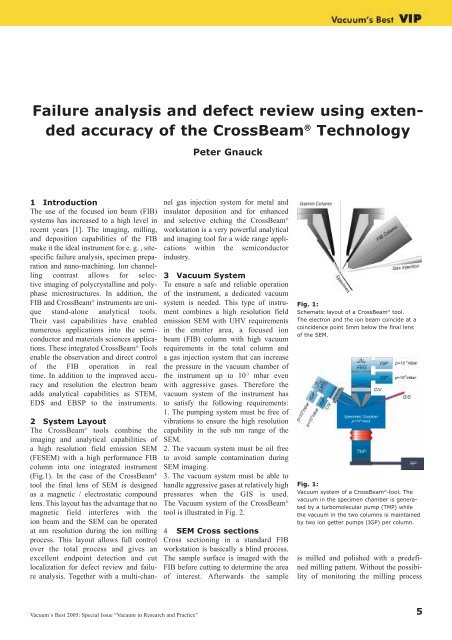
2 System Layout<br />
The CrossBeam ® tools combine the<br />
imaging <strong>and</strong> analytical capabilities of<br />
a high resolution field emission SEM<br />
(FESEM) with a high performance FIB<br />
column into one integrated instrument<br />
(Fig.1). In the case of the CrossBeam ®<br />
tool the final lens of SEM is designed<br />
as a magnetic / electrostatic compound<br />
lens. This layout has the advantage that no<br />
magnetic field interferes with the<br />
ion beam <strong>and</strong> the SEM can be operated<br />
at nm resolution during the ion milling<br />
process. This layout allows full control<br />
over the total process <strong>and</strong> gives an<br />
excellent endpoint detection <strong>and</strong> cut<br />
localization for <strong>defect</strong> <strong>review</strong> <strong>and</strong> failure<br />
<strong>analysis</strong>. Together with a multi-chan-<br />
Vacuum´s Best 2005: Special Issue “Vacuum in Research <strong>and</strong> Practice”<br />
Peter Gnauck<br />
nel gas injection system for metal <strong>and</strong><br />
insulator deposition <strong>and</strong> for enhanced<br />
<strong>and</strong> selective etching the CrossBeam ®<br />
workstation is a very powerful analytical<br />
<strong>and</strong> imaging tool for a wide range applications<br />
within the semiconductor<br />
industry.<br />
3 Vacuum System<br />
To ensure a safe <strong>and</strong> reliable operation<br />
of the instrument, a <strong>ded</strong>icated vacuum<br />
system is nee<strong>ded</strong>. This type of instrument<br />
combines a high resolution field<br />
emission SEM with UHV requirements<br />
in the emitter area, a focused ion<br />
beam (FIB) column with high vacuum<br />
requirements in the total column <strong>and</strong><br />
a gas injection system that can increase<br />
the pressure in the vacuum chamber of<br />
the instrument up to 10 -3 mbar even<br />
with aggressive gases. Therefore the<br />
vacuum system of the instrument has<br />
to satisfy the following requirements:<br />
1. The pumping system must be free of<br />
vibrations to ensure the high resolution<br />
capability in the sub nm range of the<br />
SEM.<br />
2. The vacuum system must be oil free<br />
to avoid sample contamination during<br />
SEM imaging.<br />
3. The vacuum system must be able to<br />
h<strong>and</strong>le aggressive gases at relatively high<br />
pressures when the GIS is used.<br />
The Vacuum system of the CrossBeam ®<br />
tool is illustrated in Fig. 2.<br />
4 SEM Cross sections<br />
Cross sectioning in a st<strong>and</strong>ard FIB<br />
workstation is basically a blind process.<br />
The sample surface is imaged with the<br />
FIB before cutting to determine the area<br />
of interest. Afterwards the sample<br />
Fig. 1:<br />
Schematic layout of a CrossBeam ® tool.<br />
The electron <strong>and</strong> the ion beam coincide at a<br />
coincidence point 5mm below the final lens<br />
of the SEM.<br />
Fig. 1:<br />
Vacuum system of a CrossBeam ® -tool. The<br />
vacuum in the specimen chamber is generated<br />
by a turbomolecular pump (TMP) while<br />
the vacuum in the two columns is maintained<br />
by two ion getter pumps (IGP) per column.<br />
is milled <strong>and</strong> polished with a predefined<br />
milling pattern. Without the possibility<br />
of monitoring the milling process<br />
5
Fig. 3:<br />
Three dimensional <strong>analysis</strong> of a semiconductor<br />
device. The image was taken during<br />
ion milling.<br />
Fig. 5:<br />
Steps for a pre thinned TEM sample preparation <strong>using</strong> the CrossBeam ® technology. In step<br />
1 the sample is milled <strong>and</strong> polished from the first side under continuous SEM control.<br />
In the second step the sample is rotated by 180° <strong>and</strong> the backside of the sample is milled<br />
<strong>and</strong> polished under continuous SEM control until the desired thickness is achieved.<br />
Fig. 7:<br />
TEM lift out sample preparation <strong>using</strong> the CrossBeam ® technology After the final polish the<br />
lamella is cut out of the substrate by three cuts <strong>and</strong> is transferred to a TEM grid by use of a<br />
micromanipulator <strong>and</strong> a glass needle.<br />
directly the area of interest can easily<br />
be destroyed.<br />
The unique capability of the CrossBeam ®<br />
tools to image the sample in real time<br />
at high resolution during the ion<br />
milling process gives the operator<br />
a direct interactive control to the ion<br />
milling process (Fig 3). This results in an<br />
<strong>exten</strong><strong>ded</strong> accuracy on site specific<br />
cross sections. The milling <strong>and</strong> poli-<br />
6<br />
Fig. 4:<br />
Cross section through tungsten plugs in a<br />
semiconductor device. The image was taken<br />
during ion milling. The milling process can be<br />
stopped exactly in the centre of the plugs.<br />
shing process can be directly imaged <strong>and</strong><br />
stopped exactly at the detail of interest<br />
(Fig.4).<br />
Especially in the case of TEM sample<br />
preparation the danger of destroying<br />
the fine lamella is reduced to a minimum.<br />
Another advantage of the CrossBeam ®<br />
technology is the time saving cut <strong>and</strong><br />
see operation: The sample is imaged<br />
Fig. 6:<br />
TEM sample during ion milling. The lamella<br />
can be positioned exactly at the area of interest.<br />
Note the electron transparency of the<br />
thin area.<br />
during or immediately after the polishing.<br />
This results in extremely short<br />
inspection times for each cross section.<br />
In addition avi movies that are recor<strong>ded</strong><br />
during the cutting process can be<br />
used for three dimensional reconstruction<br />
of the sample.<br />
5 TEM Sample Preparation<br />
Several TEM sample preparation techniques<br />
<strong>using</strong> FIB, such as pre-thinning<br />
(Fig. 5) <strong>and</strong> lift-out techniques (Fig. 7,<br />
8) have been published [2-4]. The FIB<br />
lift-out technique allows thin membranes<br />
to be extracted from bulk material,<br />
which saves a lot of sample pre-thinning<br />
time <strong>and</strong> is very successful in the preparation<br />
of site specific cross sections <strong>and</strong><br />
planar samples. However TEM sample<br />
preparation can be automated by <strong>using</strong><br />
scripts <strong>and</strong> macros the best accuracy is<br />
achieved if the milling is done manually<br />
with direct SEM observation. (Keep in<br />
mind that an automated process is a<br />
blind process). In a first step the sample<br />
is milled <strong>and</strong> polished from the front<br />
side under continuous SEM control<br />
until the detail of interest is visible. In<br />
the second step the sample is rotated by<br />
180° <strong>and</strong> the backside of the sample is<br />
milled <strong>and</strong> polished under continuous<br />
SEM control until the desired thickness<br />
is achieved (Fig. 6).<br />
By imaging the TEM sample in the SEM<br />
the danger of destroying the TEM lamella<br />
due to drift etc. is minimized. Another<br />
opportunity of the direct SEM imaging<br />
is a very straight control of the specimen<br />
thickness <strong>and</strong> electron transparency<br />
during the ion milling process (Fig.6).
Fig. 8:<br />
TEM lift out sample after milling <strong>and</strong> polishing.<br />
The sample is cut out of the substrate<br />
an is ready for lift out Note the electron<br />
transparency of the thin area.<br />
The best result concerning time <strong>and</strong><br />
accuracy is achieved if different samples<br />
are pre-thinned automatically overnight<br />
to a thickness of about 1µm <strong>and</strong> then<br />
polished manually under high resolution<br />
SEM observation.<br />
6 STEM imaging<br />
By inserting a multimode STEM-detector<br />
into the instrument <strong>analysis</strong> on<br />
a sub nm level is possible. Together<br />
with the real time imaging capabilities<br />
extremely accurate <strong>and</strong> site specific<br />
cross sections can be performed <strong>and</strong><br />
Fig. 9:<br />
30 kV bright field STEM image of a Semiconductor<br />
structure A very small <strong>defect</strong> was<br />
exactly hit in the centre.<br />
analyzed at a sub an level. Fig. 6 display<br />
an example of a sub µm <strong>defect</strong> in<br />
a semiconductor sample that could be<br />
located by <strong>using</strong> the live imaging possibilities<br />
of the CrossBeam ® . The image<br />
was taken <strong>using</strong> the STEM mode of the<br />
CrossBeam ® system.<br />
References<br />
[1] J. Orloff, Rev. Sci. Instr. 64, 1993, p. 1150 ff<br />
[2] L. R. Herlinger, S. Chevacharoenkul, D. C.<br />
Erwin, ISTFA 1996, p415<br />
[3] R. Rai, S. Subramanian, S. Rose, J. Conner,<br />
P. Schani, J. Moss, ISTFA 2000, p415<br />
[4] T. L. Shofner, J. L. Drown, S. R. Brown,<br />
B. B. Rossie, M. A. Decker, Y. S. Obeng,<br />
F. A. Stevie, ISTFA 2000, p45<br />
Author<br />
Dr. Peter Gnauck<br />
1995 Diploma in Physics, University of<br />
Tuebingen, Germany<br />
1995-1999 Research Scientist at NMI,<br />
Reutlingen, Germany<br />
2000 PhD in Physics, University of<br />
Tuebingen, Germany<br />
1999-2001 Project Manager in the R+D<br />
department at LEO Electron Microscopy<br />
Group<br />
since 2001 Product Manager for<br />
CrossBeam ® Systems at <strong>Carl</strong> <strong>Zeiss</strong> NTS<br />
Kontakt:<br />
Dr. Peter Gnauck,<br />
<strong>Carl</strong> <strong>Zeiss</strong> NTS GmbH,<br />
73446 Oberkochen, Germany,<br />
email: Gnauck@smt.zeiss.com<br />
TEM Lamella prepared of a<br />
DRAM device on a selected spot.<br />
The material is milled away <strong>and</strong><br />
polished with an ion-beam on both<br />
sides of the thin TEM specimen.<br />
The whole process is under constant<br />
observation with an scanning electron<br />
beam to guarantee optimum quality.<br />
(<strong>Carl</strong> <strong>Zeiss</strong> SMT, Oberkochen)<br />
7
`êçëë_É~ã∆ Ó=<br />
qÜÉ=räíáã~íÉ=PJa=oÉëÉ~êÅÜ=qççä<br />
Enabling the Nano-Age World ®<br />
<strong>Carl</strong> <strong>Zeiss</strong> SMT<br />
Nano Technology Systems Division<br />
<strong>Carl</strong>-<strong>Zeiss</strong>-Str. 56<br />
73447 Oberkochen<br />
Germany<br />
<strong>Carl</strong> <strong>Zeiss</strong> SMT – Nano Technology Systems Division<br />
Tel. +4973 64 / 20 44 88<br />
Fax +4973 64 / 20 43 43<br />
info-nts@smt.zeiss.com<br />
www.smt.zeiss.com/nts<br />
Only the 1540 XB CrossBeam ®<br />
offers the combination of ultra high<br />
resolution, simultaneous imaging,<br />
distortion-free <strong>analysis</strong> of magnetic<br />
specimens <strong>and</strong> a compact<br />
multi-channel gas injection system.<br />
It’s the ideal workstation for all<br />
your ion milling, TEM sample prep<br />
<strong>and</strong> high resolution SEM imaging<br />
requirements.