CH1-silicon wafer & Si epitaxy - KTH
CH1-silicon wafer & Si epitaxy - KTH
CH1-silicon wafer & Si epitaxy - KTH
- TAGS
- wafer
- epitaxy
- www.it.kth.se

You also want an ePaper? Increase the reach of your titles
YUMPU automatically turns print PDFs into web optimized ePapers that Google loves.
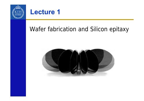
Lecture 1<br />
Wafer fabrication and <strong>Si</strong>licon <strong>epitaxy</strong>
2B1242 SPRING 2006<br />
<strong>Si</strong>licon <strong>wafer</strong> fabrication<br />
Mikael Östling <strong>KTH</strong><br />
Mag.
2B1242 SPRING 2006<br />
Wafer fabrication<br />
Starting material: Electronically-grade <strong>Si</strong> (EGS) with contamination<br />
below ppb level<br />
Czochralski method<br />
Mikael Östling <strong>KTH</strong>
2B1242 SPRING 2006<br />
Standard for CMOS.<br />
Dash method for moving dislocations out from the surface at the pulling<br />
seed.<br />
300 mm <strong>wafer</strong>s : Multi-wire slicing. <strong>Si</strong>ngle-<strong>wafer</strong> lapping. Notch marking<br />
replaces major/minor flats.<br />
Dopant incorporation: Segregation coefficient k 0 = C Solid /C liquid<br />
(Plummer Fig. 3.18 p 128)<br />
Mikael Östling <strong>KTH</strong>
2B1242 SPRING 2006<br />
Float-zone method<br />
No crucible, crystal formed in Ar atmosphere<br />
Low oxygen content<br />
High-resistivity possible<br />
Neutron Transmutation Doping for extremely high-uniform<br />
resistivity<br />
Difficult to scale up in <strong>wafer</strong> diameter<br />
Mikael Östling <strong>KTH</strong>
2B1242 SPRING 2006<br />
Defects in <strong>Si</strong><br />
Point defects :<br />
V vacancy (neutral, single- or double-charged)<br />
(see further Plummer p133-138)<br />
I interstitial or interstitialcy<br />
1-D defect: dislocation<br />
2-D defect: Stacking fault<br />
3-D defect: Precipitates<br />
(oxygen precipitation)<br />
(Plummer Fig. 3-4 p 98)<br />
Mikael Östling <strong>KTH</strong>
2B1242 SPRING 2006<br />
Oxygen in CZ- <strong>Si</strong><br />
Oxygen dissolves from quartz crucible during CZ growth<br />
~10 18 cm -3 !<br />
Three effects during circuit processing :<br />
+ <strong>Si</strong>-O-<strong>Si</strong> bindings resulting in higher mechanical strength<br />
- Oxygen donors (<strong>Si</strong>O 4). 10 16 cm -3 form at 400-500 ° C<br />
- Bulk precipitation (<strong>Si</strong>O 2) (but can be controlled by gettering)<br />
Mikael Östling <strong>KTH</strong>
2B1242 SPRING 2006<br />
SOI: <strong>Si</strong>licon-on-insulator <strong>wafer</strong>s<br />
Buried oxide layer ~10 3 Åthick<br />
SIMOX: Separation by implanted oxygen<br />
BESOI: Bonded and etch-back technology<br />
Smart-cut: H implant before BESOI process<br />
SOS <strong>wafer</strong>s: <strong>Si</strong>licon-on-sapphire<br />
(SIMOX)<br />
(BESOI)<br />
Mikael Östling <strong>KTH</strong>
2B1242 SPRING 2006<br />
Gettering<br />
Capture defects at locations far away from the device region.<br />
Damaged region will act as "sink" for unwanted elements.<br />
(Plummer Fig 4-7 p 162)<br />
Mikael Östling <strong>KTH</strong>
2B1242 SPRING 2006<br />
Extrinsic gettering:<br />
Treatment on backside of <strong>wafer</strong>, e.g. n + doping<br />
Intrinsic gettering:<br />
Intentional <strong>Si</strong>O 2 precipitation inside bulk.<br />
Requires dedicated thermal cycling:<br />
(Plummer Fig 4-12)<br />
Mikael Östling <strong>KTH</strong>
2B1242 SPRING 2006<br />
<strong>Si</strong>licon <strong>epitaxy</strong><br />
Outline:<br />
Definition and terminology<br />
Chemical vapor deposition<br />
CVD process and source gases<br />
Grove model:<br />
• Mass-transfer or surface-reaction controlled growth rate<br />
Gas flow and pressure in CVD<br />
Chlorine in <strong>Si</strong> CVD<br />
Doping<br />
• Autodoping<br />
Defects and characterization<br />
Reactor types<br />
•Batch<br />
• <strong>Si</strong>ngle-<strong>wafer</strong><br />
•MBE<br />
Applications of <strong>Si</strong> <strong>epitaxy</strong><br />
• HT <strong>epitaxy</strong>: <strong>Si</strong><br />
• LT <strong>epitaxy</strong>: <strong>Si</strong>Ge<br />
• Selective <strong>epitaxy</strong>: <strong>Si</strong> and <strong>Si</strong>Ge<br />
Mikael Östling <strong>KTH</strong>
2B1242 SPRING 2006<br />
Book references cited :<br />
S.M. Sze: Semiconductor Devices 1985<br />
S-M.Sze ed: VLSI Technology 1988<br />
Chang and S.M. Sze: ULSI Technology 1996<br />
S. Wolf and R.N. Tauber: <strong>Si</strong>licon Processing for VLSI vol. 1 1986<br />
J. Plummer, <strong>Si</strong>licon VLSI Technology 2000<br />
Mikael Östling <strong>KTH</strong>
2B1242 SPRING 2006<br />
<strong>Si</strong>licon <strong>epitaxy</strong><br />
Definition<br />
Growth of single-crystalline layer on a single-crystalline substrate (bulk)<br />
Epitaxal layer thickness: From one single atom layer up to ca 100 µm<br />
Homo<strong>epitaxy</strong> : <strong>Si</strong> on <strong>Si</strong><br />
Hetero<strong>epitaxy</strong> : e.g. <strong>Si</strong>xGe1-x on <strong>Si</strong><br />
Doping level can vary substantially between the layer and bulk<br />
Advantages with <strong>epitaxy</strong>:<br />
Lower temperature compared to implantation + diffusion �<br />
much more abrupt doping profiles<br />
Large interval of thicknesses, doping profiles, and band gap engineering �<br />
ideal for creating "artificial" semiconductor structures, e.g. HBTs, HEMTs<br />
Mikael Östling <strong>KTH</strong>
2B1242 SPRING 2006<br />
<strong>Si</strong>licon <strong>epitaxy</strong>:<br />
Conventional, or high-temperature (HT), <strong>epitaxy</strong> at T > 1000°C<br />
(on blanket or patterned <strong>wafer</strong>s)<br />
Low-temperature (LT or LTE) <strong>epitaxy</strong> at T < 1000°C.<br />
(Usually on patterned substrates)<br />
Selective <strong>epitaxy</strong> (always on patterned substrates)<br />
Terminology for CVD <strong>Si</strong>Ge <strong>epitaxy</strong>:<br />
Selective epitaxial growth: SEG<br />
Non-selective epitaxial growth: NSEG<br />
Mikael Östling <strong>KTH</strong>
2B1242 SPRING 2006<br />
Hetero<strong>epitaxy</strong> (<strong>Si</strong>Ge on <strong>Si</strong>)<br />
Strained growth conditions, so-called pseudomorphic growth<br />
h c = critical thickness<br />
Unstrained � dislocation network which are adverse for device<br />
operation<br />
g p.106<br />
(Chang p.106)<br />
Mikael Östling <strong>KTH</strong><br />
Chan
2B1242 SPRING 2006<br />
Technology of choice for <strong>Si</strong> epitaxial growth in production environment:<br />
Chemical vapor deposition (CVD)<br />
(sometimes denoted vapor phase <strong>epitaxy</strong>(VPE))<br />
Hydrogen (H 2 ) carrier gas<br />
Reactants: <strong>Si</strong>Cl 4 , <strong>Si</strong>HCl 3 , <strong>Si</strong>H 4 , + dopant gases (AsH 3 , B2H 6 …)<br />
HCl for selective growth and/or chamber cleaning<br />
N 2 for purge<br />
Mikael Östling <strong>KTH</strong>
2B1242 SPRING 2006<br />
Basic <strong>Si</strong> CVD types (both batch and single-<strong>wafer</strong> rectors)<br />
APCVD (atmospheric pressure CVD)<br />
Only for HT <strong>epitaxy</strong> (e.g. p-<strong>epitaxy</strong> on p+ bulk)<br />
LPCVD (low-pressure CVD)<br />
Deposition around 10-100 torr, e.g. for n+ HT <strong>epitaxy</strong>,<br />
LT <strong>Si</strong>Ge <strong>epitaxy</strong> or SEG<br />
UHVCVD (ultra-high vacuum CVD)<br />
Deposition around 10-3 torr. For LT <strong>Si</strong>Ge <strong>epitaxy</strong><br />
(NSEG)<br />
Mikael Östling <strong>KTH</strong>
2B1242 SPRING 2006<br />
CVD process<br />
1. Transport of reactants to the deposition region<br />
2. Transport of reactants by diffusion from the main gas stream through the<br />
boundary layer to the <strong>wafer</strong> surface<br />
3. Adsorption of reactants on the <strong>wafer</strong> surface<br />
4. Surface processes: migration, decomposition, reaction, site incorporation<br />
5. Desorption of byproducts from surface<br />
6. Transport of byproducts through the boundary layer<br />
7. Transport of byproducts from the deposition region<br />
(Plummer Fig 9-5 p 514)<br />
(Sze Fig 19 p323)<br />
Mikael Östling <strong>KTH</strong>
2B1242 SPRING 2006<br />
<strong>Si</strong> CVD sources and basic reactions for HT <strong>epitaxy</strong><br />
<strong>Si</strong>licontetrachloride: <strong>Si</strong>Cl 4 + H 2 ⇔ <strong>Si</strong> + 4HCl (~1200°C)<br />
Trichlorosilane (TCS): <strong>Si</strong>HCl 3 + H 2 ⇔ <strong>Si</strong> + 3HCl (~1150°C)<br />
Dichlorosilane (DCS): <strong>Si</strong>HCl 2 ⇔ <strong>Si</strong> + 2HCl (~1100°C)<br />
<strong>Si</strong>lane: <strong>Si</strong>H 4 ⇒ <strong>Si</strong> + 2H 2 (~1050°C)<br />
HT <strong>epitaxy</strong>: TCS or DCS<br />
LT <strong>epitaxy</strong>: DCS or silane<br />
(Sze VLSI Table I p. 65 )<br />
Mikael Östling <strong>KTH</strong>
2B1242 SPRING 2006<br />
The Grove model for epitaxial growth<br />
Growth limited by mass-transfer or surface reaction<br />
F<br />
F<br />
1<br />
2<br />
=<br />
=<br />
h<br />
k<br />
g<br />
s<br />
( C<br />
C<br />
s<br />
g<br />
− C<br />
h g = vapor mass transfer coefficient<br />
k s = surface reaction constant<br />
s<br />
)<br />
Assume:<br />
Steady state: F 1 =F 2 = F<br />
Growth rate n = F/C a where C a = number of <strong>Si</strong> atoms/cm 3<br />
(Sze Fig. 20 p 324)<br />
C g = yC t where y is the mole fraction and C t is the total number of gas molec/cm 3 �<br />
kshg<br />
v =<br />
k + h<br />
⎞<br />
⎟ y<br />
⎠<br />
k s small � Surface reaction controlled<br />
h g small � Mass-transport controlled<br />
s<br />
g<br />
⎛ Ct<br />
⎜<br />
⎝ Ca<br />
C t k s y<br />
C ⎟<br />
a<br />
⎟<br />
⎛ ⎞<br />
⎜<br />
⎝ ⎠<br />
Mikael Östling <strong>KTH</strong><br />
v<br />
v<br />
≅<br />
≅<br />
h<br />
g<br />
⎛<br />
⎜<br />
⎝<br />
C<br />
C<br />
t<br />
a<br />
⎞<br />
⎟<br />
⎠<br />
y
2B1242 SPRING 2006<br />
Consequences:<br />
(Plummer Fig 9-7)<br />
(Sze Fig 21 p. 326 )<br />
Mikael Östling <strong>KTH</strong>
2B1242 SPRING 2006<br />
Gas flow rate<br />
Mass-transport controlled regime<br />
Laminar gas flow with velocity v above a boundary layer with thickness δ<br />
(Sze Fig. 22 p.327 )<br />
Analysis of friction force � h g =D g /d ~ √v<br />
where D G is gas diffusion coefficient across δ<br />
(Chang Fig 7 p 114 )<br />
Mikael Östling <strong>KTH</strong>
2B1242 SPRING 2006<br />
Surface reaction controlled regime:<br />
Deposition not (very) sensitive to geometrical arrangement of <strong>wafer</strong>s in reactor.<br />
However, low growth rates!<br />
Can be solved by reducing total pressure which affects D G and extends surfacereaction<br />
limited region to higher T:<br />
(Plummer Fig 9-13)<br />
Mikael Östling <strong>KTH</strong>
2B1242 SPRING 2006<br />
<strong>Si</strong> epi-growth rate for Cl-based chemistry<br />
Either deposition or etching depending on T, P or concentration (mole<br />
Fraction)<br />
Reaction is complex, e.g. <strong>Si</strong>Cl 4 :<br />
<strong>Si</strong>Cl 4 + H 2 ⇔ <strong>Si</strong>HCl 3 + HCl <strong>Si</strong>HCl 3 ⇔ <strong>Si</strong>Cl 2 + HCl<br />
<strong>Si</strong>HCl 3 + H 2 ⇔ <strong>Si</strong>H 2 Cl 2 + HCl <strong>Si</strong>Cl 2 + H 2 ⇔ <strong>Si</strong> + 2HCl<br />
<strong>Si</strong>H 2 Cl 2 ⇔ <strong>Si</strong>Cl 2 + H 2<br />
Mikael Östling <strong>KTH</strong>
2B1242 SPRING 2006<br />
Reversible reactions!<br />
(Sze p. 322)<br />
Crystallinity also depends on growth rate:<br />
(Chang Fig 10 p)<br />
Mikael Östling <strong>KTH</strong>
2B1242 SPRING 2006<br />
Doping in <strong>Si</strong> <strong>epitaxy</strong><br />
Doping sources: B 2 H 6 (diborane), AsH 3 (arsine) and PH 3 (phosphine).<br />
Not standard: SbCl 5<br />
Dopant incorporation dependent upon T, growth rate, dopant/<strong>Si</strong> ratio<br />
in gas phase, reactor geometry<br />
B 2 H 6 enhances growth rate<br />
PH 3 reduced growth rate<br />
Example from <strong>KTH</strong>:<br />
Double-epi (n - /n + ) using AsH 3 on p - bulk<br />
Radamson & Grahn 98<br />
Mikael Östling <strong>KTH</strong>
2B1242 SPRING 2006<br />
Autodoping<br />
Lightly doped n-epi-layer grown on n + substrate �<br />
autodoping, i.e. unintentional doping from substrate, susceptor, adjacent <strong>wafer</strong>s etc.<br />
Both vertical and lateral autodoping may<br />
occur , e.g. during <strong>epitaxy</strong> on buried n + -<br />
layer<br />
Remedies:<br />
Low-pressure CVD for HT n-type epi<br />
Reduced deposition temperature<br />
Observe: Autodoping is not a problem for B!<br />
(Chang Fig 16 p. 120 )<br />
Mikael Östling <strong>KTH</strong>
2B1242 SPRING 2006<br />
Defects in epitaxial layers<br />
(Sze VLSI Fig. 20 p 76 )<br />
Dislocations (line defect)<br />
Stacking faults (area defect) visible as squares for (100) and triangles for (111)<br />
Precipitates (volume defect)<br />
Hillocks or voids (volume defects)<br />
Substrate surface quality and cleaning prior to <strong>epitaxy</strong> are crucial, in particular LT<br />
<strong>epitaxy</strong>.<br />
Slip in HT <strong>epitaxy</strong>:<br />
Dislocation network caused by temperature gradient across <strong>wafer</strong> during RTA-CVD<br />
(single-<strong>wafer</strong> machines)<br />
Mikael Östling <strong>KTH</strong>
2B1242 SPRING 2006<br />
Epi thin film characterization<br />
Surface smoothness:<br />
Optical microscopy<br />
Nomarski contrast microscopy<br />
Atomic force microscopy (AFM)<br />
Film thickness and doping:<br />
Secondary ion mass spectroscopy (SIMS)<br />
Fourier-transform Infrared Spectroscopy (FTIR) (see below)<br />
Crystallographic quality:<br />
High-resolution X-ray diffractometry for Ge content and thickness in <strong>Si</strong>Ge<br />
Electrical properties:<br />
Film resistivity vs doping<br />
Minority carrier life time measurment<br />
Device characteristic<br />
(Wolf Fig 24 p 151 )<br />
Mikael Östling <strong>KTH</strong>
2B1242 SPRING 2006<br />
Reactor types for <strong>Si</strong> <strong>epitaxy</strong><br />
Batch reactor types<br />
Almost only for HT <strong>epitaxy</strong> (exception UHVCVD)<br />
(Chang Fig. 20 p124 )<br />
Mikael Östling <strong>KTH</strong>
2B1242 SPRING 2006<br />
Example of batch type epi-reactors:<br />
Mikael Östling <strong>KTH</strong>
2B1242 SPRING 2006<br />
<strong>Si</strong>ngle-<strong>wafer</strong> <strong>Si</strong> <strong>epitaxy</strong><br />
RTP process!<br />
Both for HT and LT <strong>epitaxy</strong> (<strong>Si</strong>/<strong>Si</strong>Ge)<br />
Used for production of <strong>wafer</strong>s, epi on buried layers and LT epi <strong>Si</strong>Ge.<br />
Example:<br />
(ASM Epsilon 2000 at <strong>KTH</strong>)<br />
Mikael Östling <strong>KTH</strong>
2B1242 SPRING 2006<br />
UHVCVD<br />
LT non-selective epi method developed by IBM specially for <strong>Si</strong>Ge<br />
Batch method at very low temperature 500-600°C<br />
(Chang Fig 22 p 128 )<br />
Mikael Östling <strong>KTH</strong>
2B1242 SPRING 2006<br />
Special <strong>wafer</strong> cleaning developed, so-called hydrogen termination of <strong>Si</strong><br />
surface using an HF dip prior to loading.<br />
No in situ surface cleaning!<br />
(Chang Fig 23 p129)<br />
Mikael Östling <strong>KTH</strong>
2B1242 SPRING 2006<br />
<strong>Si</strong>licon Molecular Beam Epitaxy (MBE)<br />
Physical vapor deposition (PVD) method<br />
Typical for thin film research for <strong>Si</strong>Ge(C) <strong>epitaxy</strong> (not in production!)<br />
Vacuum evaporation with excellent thickness control<br />
Ultra-high vacuum<br />
Extremely low growth temperatures < 500°C<br />
In situ analysis of growing film<br />
As and, in particular, Ph dopants difficult. Often Sb for n+<br />
(Sze VLSI Fig 23 p.80 )<br />
Mikael Östling <strong>KTH</strong>
2B1242 SPRING 2006<br />
Applications of <strong>Si</strong> <strong>epitaxy</strong><br />
HT <strong>epitaxy</strong>:<br />
p- epi on p+ bulk in CMOS for suppression of latch-up<br />
n- on n+ buried collector layer in bipolar devices for reduced series resistance<br />
(single- or double epi):<br />
p +<br />
n -<br />
P plug<br />
n+ buried layer<br />
LOCOS isolation<br />
Mikael Östling <strong>KTH</strong><br />
p +<br />
Grahn ASM User meeting’99<br />
Problem: Pattern shift during n-epi on buried layer<br />
Important to control for <strong>wafer</strong> alignment<br />
on buried layer!<br />
(Chang p.123)
2B1242 SPRING 2006<br />
LT <strong>epitaxy</strong>:<br />
<strong>Si</strong>Ge epi for base in bipolars, channel for MOS<br />
Example: <strong>KTH</strong> <strong>Si</strong>Ge HBT using NSEG <strong>Si</strong>Ge<br />
p +<br />
Base Emitter Collector<br />
Poly<br />
x-base<br />
<strong>Si</strong>Ge epitaxial base<br />
n -<br />
n+ buried layer<br />
Poly emitter<br />
LTO oxide<br />
LOCOS isolation<br />
Mikael Östling <strong>KTH</strong><br />
P plug<br />
Concentration ( cm -3 )<br />
10 22<br />
10 21<br />
10 20<br />
10 19<br />
10 18<br />
10 17<br />
10 16<br />
Aluminum<br />
Poly<br />
P<br />
B<br />
p +<br />
Epi<br />
Grahn et al SSE’’00<br />
Ge<br />
2<br />
0 1000 2000 3000<br />
Depth<br />
14<br />
12<br />
10<br />
8<br />
6<br />
4<br />
Ge (%)
2B1242 SPRING 2006<br />
<strong>Si</strong>Ge LT <strong>epitaxy</strong><br />
Typically at 550-650°C using UHVCVD, LPCVD or APCVD<br />
Selective or non-selective growth<br />
Selective or non-selective growth<br />
de Boer MRS 94<br />
Mikael Östling <strong>KTH</strong>
2B1242 SPRING 2006<br />
<strong>Si</strong> SEG<br />
Conventional chemistry:<br />
Addition of HCl to DCS makes <strong>Si</strong> epi selective with respect to field oxide<br />
SEG is a difficult process in VLSI!<br />
STI isolation is the preferred process choice<br />
Mikael Östling <strong>KTH</strong>
2B1242 SPRING 2006<br />
<strong>Si</strong>Ge SEG<br />
Selective epitaxial growth (SEG) of <strong>Si</strong>Ge in a double-poly bipolar process<br />
<strong>Si</strong>Ge is self-aligned to the base poly overhang<br />
Infineon B7HF (Meister IEDM '95)<br />
Mikael Östling <strong>KTH</strong>
2B1242 SPRING 2006<br />
Advanced LT <strong>epitaxy</strong><br />
Epitaxial lateral overgrowth (ELO)<br />
Adding methylsilane (CH 3 <strong>Si</strong>H 3 ) to <strong>Si</strong>Ge <strong>epitaxy</strong> for <strong>Si</strong>GeC<br />
HBTs<br />
Examples:<br />
<strong>Si</strong> npn using LTE base + ELO for base poly<br />
From J. Burghartz, IBM<br />
Mikael Östling <strong>KTH</strong>
2B1242 SPRING 2006<br />
<strong>Si</strong>Ge (C) HBT using SEGcollector and NSEG<br />
<strong>Si</strong>Ge(C)<br />
<strong>Si</strong> CMP intermediate step between<br />
SEG and NSEG<br />
On-going <strong>KTH</strong> research project together<br />
with MIC<br />
Oxide<br />
n + -poly<br />
n-SEG<br />
Mikael Östling <strong>KTH</strong><br />
FOX<br />
NSEG p + -<strong>Si</strong>Ge<br />
n +