CH1-silicon wafer & Si epitaxy - KTH
CH1-silicon wafer & Si epitaxy - KTH
CH1-silicon wafer & Si epitaxy - KTH
- TAGS
- wafer
- epitaxy
- www.it.kth.se

You also want an ePaper? Increase the reach of your titles
YUMPU automatically turns print PDFs into web optimized ePapers that Google loves.
2B1242 SPRING 2006<br />
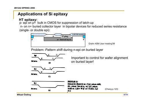
Applications of <strong>Si</strong> <strong>epitaxy</strong><br />
HT <strong>epitaxy</strong>:<br />
p- epi on p+ bulk in CMOS for suppression of latch-up<br />
n- on n+ buried collector layer in bipolar devices for reduced series resistance<br />
(single- or double epi):<br />
p +<br />
n -<br />
P plug<br />
n+ buried layer<br />
LOCOS isolation<br />
Mikael Östling <strong>KTH</strong><br />
p +<br />
Grahn ASM User meeting’99<br />
Problem: Pattern shift during n-epi on buried layer<br />
Important to control for <strong>wafer</strong> alignment<br />
on buried layer!<br />
(Chang p.123)