CH1-silicon wafer & Si epitaxy - KTH
CH1-silicon wafer & Si epitaxy - KTH
CH1-silicon wafer & Si epitaxy - KTH
- TAGS
- wafer
- epitaxy
- www.it.kth.se

Create successful ePaper yourself
Turn your PDF publications into a flip-book with our unique Google optimized e-Paper software.
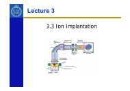
2B1242 SPRING 2006<br />
<strong>Si</strong>licon <strong>epitaxy</strong><br />
Definition<br />
Growth of single-crystalline layer on a single-crystalline substrate (bulk)<br />
Epitaxal layer thickness: From one single atom layer up to ca 100 µm<br />
Homo<strong>epitaxy</strong> : <strong>Si</strong> on <strong>Si</strong><br />
Hetero<strong>epitaxy</strong> : e.g. <strong>Si</strong>xGe1-x on <strong>Si</strong><br />
Doping level can vary substantially between the layer and bulk<br />
Advantages with <strong>epitaxy</strong>:<br />
Lower temperature compared to implantation + diffusion �<br />
much more abrupt doping profiles<br />
Large interval of thicknesses, doping profiles, and band gap engineering �<br />
ideal for creating "artificial" semiconductor structures, e.g. HBTs, HEMTs<br />
Mikael Östling <strong>KTH</strong>