CH1-silicon wafer & Si epitaxy - KTH
CH1-silicon wafer & Si epitaxy - KTH
CH1-silicon wafer & Si epitaxy - KTH
- TAGS
- wafer
- epitaxy
- www.it.kth.se

Create successful ePaper yourself
Turn your PDF publications into a flip-book with our unique Google optimized e-Paper software.
2B1242 SPRING 2006<br />
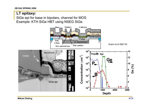
LT <strong>epitaxy</strong>:<br />
<strong>Si</strong>Ge epi for base in bipolars, channel for MOS<br />
Example: <strong>KTH</strong> <strong>Si</strong>Ge HBT using NSEG <strong>Si</strong>Ge<br />
p +<br />
Base Emitter Collector<br />
Poly<br />
x-base<br />
<strong>Si</strong>Ge epitaxial base<br />
n -<br />
n+ buried layer<br />
Poly emitter<br />
LTO oxide<br />
LOCOS isolation<br />
Mikael Östling <strong>KTH</strong><br />
P plug<br />
Concentration ( cm -3 )<br />
10 22<br />
10 21<br />
10 20<br />
10 19<br />
10 18<br />
10 17<br />
10 16<br />
Aluminum<br />
Poly<br />
P<br />
B<br />
p +<br />
Epi<br />
Grahn et al SSE’’00<br />
Ge<br />
2<br />
0 1000 2000 3000<br />
Depth<br />
14<br />
12<br />
10<br />
8<br />
6<br />
4<br />
Ge (%)