
You also want an ePaper? Increase the reach of your titles
YUMPU automatically turns print PDFs into web optimized ePapers that Google loves.
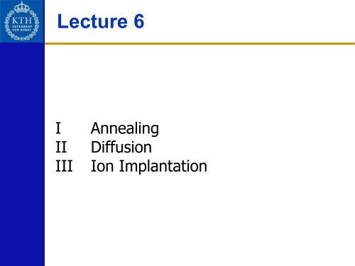
<strong>Lecture</strong> 6<br />
I Annealing<br />
II Diffusion<br />
III Ion Implantation
“Where we are today”<br />
Wafer Fabrication<br />
FEOL Processes<br />
PS: This list of co-dependencies is<br />
not complete!<br />
BEOL Fabrication<br />
Packaging<br />
Device Integration<br />
Simulation & Modeling<br />
Metrology<br />
Electrical Testing<br />
Future Technologies
<strong>Lecture</strong> 6<br />
I Annealing<br />
II Diffusion<br />
III Ion Implantation
<strong>Lecture</strong> 6<br />
Annealing<br />
Furnace Anneal (FA), Rapid Thermal Anneal (RTA), Laser Spike Anneal (LSA)
IH2655 Spring 2011<br />
Doping in Silicon Technology<br />
“Introducing a certain number and type of impurities into<br />
silicon with accurate doping profile.”<br />
Examples:<br />
NMOS<br />
p well<br />
Applications:<br />
BJT<br />
B E C<br />
p n+ n+<br />
p+ n- p+<br />
n+<br />
MOSFET: Well, Gate, Source/Drain, Channel, etc.<br />
BJT: Base, Emitter, Collector, etc.<br />
Christoph Henkel / Mikael Östling KTH 5<br />
p
IH2655 Spring 2011<br />
Doping in Silicon Technology<br />
MOSFET: Requirements on doping<br />
�Junction Depth x j<br />
�Sheet Resistance R s<br />
�Solubility<br />
Christoph Henkel / Mikael Östling KTH 6
IH2655 Spring 2011<br />
Doping in Silicon Technology: Requirements<br />
Junction Depth x i<br />
x j : At the position x = x j , C x (Diffused Impurity Concentration) = C B<br />
(Bulk Concentration)<br />
�When devices are scaled down by a factor of k, constant-field<br />
scaling principle requires x j should also be scaled down by k.<br />
Simultaneously,<br />
�Increased control over x j is required �Short Channel Effects, DIBL<br />
(drain induced barrier lowing)<br />
In modern CMOS technology, shallow junction and highconcentration<br />
doping are used to meet both the two requirements<br />
Christoph Henkel / Mikael Östling KTH 7
IH2655 Spring 2011<br />
Thermal Budget Crisis<br />
• ITRS dictates scaling demands<br />
• Technology needs to provide solutions to avoid SCEs)<br />
• E.g. Annealing is critical for formation of shallow junctions<br />
Christoph Henkel / Mikael Östling KTH 8
IH2655 Spring 2011<br />
Annealing Technology: Overview<br />
Source: www.semiconwest.com, J. Hebb, “Laser Spike Annealing: Meeting challenges for sub-40nm CMOS devices”, Ultratech<br />
Christoph Henkel / Mikael Östling KTH<br />
9
IH2655 Spring 2011<br />
Furnace Anneal (FA)<br />
• Horizontal furnaces have now largely been replaced by vertical furnaces<br />
• Example: ASM Advance 400 series<br />
• Furnace anneal can not meet thermal budget requirements. Alternatives?<br />
• Rapid thermal heating for rates of 10-100 C/s<br />
Christoph Henkel / Mikael Östling KTH 10
IH2655 Spring 2011<br />
Rapid Thermal Anneal (RTA)<br />
• Ramp rate: 50-300 C°/s<br />
• Largest concern: Temperature control<br />
• Temperature non-uniformity due to<br />
varying emissivity<br />
Christoph Henkel / Mikael Östling KTH 11
IH2655 Spring 2011<br />
Rapid Thermal Anneal (RTA)<br />
RTA is used for:<br />
• Anneal and ultra-shallow junction<br />
formation<br />
• Oxidation (RTO)<br />
• Silicon epitaxy (in particular high-<br />
temp epi)<br />
• CVD of poly and dielectrics (e.g.<br />
Centura modules)<br />
• Silicides (Ti salicide process)<br />
• Frequently integrated in single-<br />
wafer cluster tools<br />
Christoph Henkel / Mikael Östling KTH 12
IH2655 Spring 2011<br />
Laser Thermal Annealing (LTA) / Laser Spike Anneal (LSA)<br />
Advantages of LTA/LSA<br />
• Low thermal budget<br />
• Ultra-fast annealing (< µs)<br />
• Melt vs. non-melt or submelt process<br />
• Diffusionless activation (non-melt)<br />
• E.g. non-melt millisecond laser for<br />
45nm CMOS<br />
• Used heavily in Thin Film Transistor<br />
(TFT) applications to crystallize<br />
polysilicon<br />
• For TFT, reduces temperatures from<br />
~ 1000 C to ~ 400 C<br />
Christoph Henkel / Mikael Östling KTH<br />
Non-melt (red)<br />
Source: www.excico.com<br />
“Microscale Process Uniformity by Excico LTA“<br />
13
IH2655 Spring 2011<br />
Laser Thermal Annealing (LTA) / Laser Spike Anneal (LSA)<br />
Logic device applications today … and in the future<br />
Christoph Henkel / Mikael Östling KTH<br />
Long dwell applications<br />
• Defect anneal (replace RTA<br />
spike anneal)<br />
• Stress reduction<br />
• Solid Phase Epitaxy (SPE)<br />
applications (e.g., Si:C, FINFET)<br />
Low temp applications<br />
• Nickel silicide formation<br />
(replace RTP for one or both<br />
steps)<br />
• Post silicide activation<br />
Source: www.semiconwest.com, J. Hebb, “Laser Spike Annealing: Meeting challenges for sub-40nm CMOS devices”, Ultratech<br />
14
<strong>Lecture</strong> 6<br />
I Annealing<br />
II Diffusion<br />
III Ion Implantation
IH2655 Spring 2011<br />
Diffusion in Silicon<br />
• Introduction<br />
• Dopants in Silicon Devices<br />
• Technology for diffusion<br />
• Diffusion<br />
• Solid solubility<br />
• Intrinsic diffusion and diffusion constant<br />
• Extrinsic diffusion and electrical field effect<br />
• Microscopic description<br />
• Diffusion during Thermal Oxidation<br />
• Dopant-Defect Interactions<br />
• Diffusion in polysilicon<br />
• Characterization<br />
Christoph Henkel / Mikael Östling KTH 16
IH2655 Spring 2011<br />
Introducing Dopants into Silicon<br />
In the past:<br />
Pre-deposition of dopants from gas, liquid or solid followed by diffusion ("drive-in”)<br />
Dominating since late 70's:<br />
Ion implantation of dopant ions followed by activation and crystal repair ("anneal")<br />
Diffusion<br />
Ion Implantation<br />
(Sze p. 381)<br />
Christoph Henkel / Mikael Östling KTH 17
IH2655 Spring 2011<br />
Pre-deposition of dopants: “Classical” technology<br />
Fig. 4.29 Planar source arrangement<br />
Christoph Henkel / Mikael Östling KTH 18
IH2655 Spring 2011<br />
Diffusion in Silicon<br />
• Introduction<br />
• Dopants in Silicon Devices<br />
• Technology for diffusion<br />
• Diffusion<br />
• Solid solubility<br />
• Intrinsic diffusion and diffusion constant (Fick’s Law)<br />
• Extrinsic diffusion and electrical field effect<br />
• Microscopic description<br />
• Diffusion during thermal oxidation<br />
• Dopant-Defect Interactions<br />
• Diffusion in polysilicon<br />
• Characterization<br />
Christoph Henkel / Mikael Östling KTH 19
IH2655 Spring 2011<br />
Dopant Solid Solubility<br />
� Solid solubility: The maximum concentration in equilibrium states for<br />
impurities dissolved in silicon but without any segregation phase.<br />
� Solid solubility-the maximum thermodynamic concentration<br />
� The maximum impurity concentration below which the electrical activity<br />
can be restricted/changed dynamically -electrical solid solubility<br />
� Impurities beyond electrical solid solubility may form neutral complex<br />
and hence have no contribution to carriers in the doped region<br />
n-type: P, As, Sb<br />
p-type: B, Al, Ga, Al<br />
-for most dopants<br />
highest concentration<br />
below the melting point<br />
of Si<br />
Christoph Henkel / Mikael Östling KTH 20
IH2655 Spring 2011<br />
Active and Inactive Dopants in Silicon<br />
Substituional<br />
Solid solubility of As in silicon: 2�10 21 cm -3<br />
Electrically-activable concentration of As: 2�10 20 cm -3<br />
Christoph Henkel / Mikael Östling KTH 21
IH2655 Spring 2011<br />
Intrinsic Diffusion (classical case)<br />
Fick's two diffusion laws<br />
Fick I:<br />
where D = diffusion constant (or diffusivity) [cm 2 /s]<br />
Continuity equation:<br />
Fick II:<br />
F<br />
�C<br />
�t<br />
�C<br />
� �D<br />
�x<br />
�C<br />
�F<br />
� �<br />
�t<br />
�x<br />
� � �C<br />
�<br />
�<br />
� D �<br />
�x<br />
� �x<br />
�<br />
Assume D is independent of C (and hence x) �<br />
�C<br />
�t<br />
2<br />
� C<br />
� D 2<br />
�x<br />
F = flow of atoms [cm -2 s -1 ]<br />
C= C(x,t) = dopant concentration [cm -3 ]<br />
Simple solution: no variation over time (C= a + bx, see oxidation).<br />
Boundary conditions yield two different analytical solutions for C(x,t).<br />
Christoph Henkel / Mikael Östling KTH 22<br />
(1)<br />
(2)<br />
“What goes in and does<br />
not go out, stays there.”
IH2655 Spring 2011<br />
Solution 1: Constant number of Dopants on the Surface<br />
For example from a low-energy ion implant followed by anneal<br />
C(x,0) = 0 C( � ,t) = 0<br />
�<br />
� C ( x,<br />
t ) dx<br />
0<br />
� S<br />
Solution to Eq. (2) is a Gaussian profile:<br />
C(<br />
x,<br />
t)<br />
�<br />
C s<br />
C<br />
s<br />
( t)<br />
e<br />
2<br />
�x<br />
/ 4Dt<br />
S<br />
( t)<br />
�<br />
Dt<br />
�Dt<br />
= diffusion length<br />
(Sze p 387 )<br />
Christoph Henkel / Mikael Östling KTH 23
IH2655 Spring 2011<br />
Solution 2: Infinite number of Dopants on the Surface<br />
Corresponds to a constant surface concentration (= C s )<br />
For example from a deposited chemical dopant<br />
source (POCl 3 …) followed by drive-in<br />
C(x,0) = 0 C( � ,t)=0<br />
C(0,t) = C s<br />
Solution to Eq. (2) is a so-called<br />
complementary error function erfc<br />
C( x,<br />
t)<br />
� C erfc<br />
�<br />
s �<br />
� 2<br />
erfc(<br />
z)<br />
�1<br />
�<br />
2<br />
� �<br />
z<br />
2<br />
a<br />
e da<br />
0<br />
x<br />
Dt<br />
�<br />
�<br />
�<br />
� (Sze p 387)<br />
Christoph Henkel / Mikael Östling KTH 24
IH2655 Spring 2011<br />
Diffusion: Temperature dependence<br />
D<br />
�<br />
D<br />
o<br />
e<br />
�E<br />
a<br />
/ kT<br />
Dopant diffusion in Si: E a= 3.5-4.5 eV<br />
Self-diffusion in Si: E a = 5 eV<br />
(Sze p. 384)<br />
Process Integration:<br />
Thermal budget in a process is often attributed<br />
to the Dt product. Total process thermal budget:<br />
Dt = D 1 t 1 + D 2 t 2 + D 3 t 3 + …<br />
where E a = activation energy<br />
Christoph Henkel / Mikael Östling KTH 26
IH2655 Spring 2011<br />
Extrinsic Diffusion: Concentration Dependence<br />
High impurity concentrations 10 19 - 10 20 cm -3<br />
Denoted extrinsic diffusion case since<br />
C > n i (intrinsic carrier concentration) �<br />
D = D(C) � Solution of Eq. (1) required (numerically computed)<br />
E.g. N i (T=1000ºC) = 7x10 18 cm -3<br />
(Sze p. 392)<br />
Christoph Henkel / Mikael Östling KTH 27
IH2655 Spring 2011<br />
Extrinsic Diffusion: Concentration Dependence<br />
Modifications to Fick’s law:<br />
Generalized D expression (n-type Si):<br />
0 � �<br />
��<br />
n � ��<br />
n �<br />
D � D � D<br />
�<br />
�<br />
�<br />
� � D<br />
�<br />
�<br />
� ni<br />
� � ni<br />
�<br />
Christoph Henkel / Mikael Östling KTH 28<br />
2<br />
On atomic level, D-terms are<br />
determined by neutral and<br />
charged point defects (D + for<br />
p-type)<br />
Result:<br />
"Box-like" diffusion profiles
IH2655 Spring 2011<br />
Extrinsic Diffusion: Electrical Field Effect<br />
• For extrinsic diffusion, electrical fields<br />
from dopants affect final profiles.<br />
• E.g. electrons diffuse faster than donors<br />
(Plummer p 408)<br />
(Plummer p 406)<br />
• Electrical field drags dopants into the<br />
bulk: Enhanced diffusion by a factor 1-2<br />
• Simulation example pn junction<br />
Process simulators include concentration dependence and electric field effect<br />
Christoph Henkel / Mikael Östling KTH 29
IH2655 Spring 2011<br />
Diffusion: Dopant Pileup (on addition to Segregation)<br />
Christoph Henkel / Mikael Östling KTH 30
IH2655 Spring 2011<br />
Diffusion in Silicon<br />
• Introduction<br />
• Dopants in Silicon Devices<br />
• Technology for diffusion<br />
• Diffusion<br />
• Solid solubility<br />
• Intrinsic diffusion and diffusion constant (Fick’s Law)<br />
• Extrinsic diffusion and electrical field effect<br />
• Microscopic description<br />
• Diffusion during Thermal Oxidation<br />
• Dopant-Defect Interactions<br />
• Diffusion in polysilicon<br />
• Characterization<br />
Christoph Henkel / Mikael Östling KTH 31
IH2655 Spring 2011<br />
Microscopic Description of Diffusion<br />
• The extended diffusion model is not able to explain several<br />
anomalies observed in diffusion of impurities in Si.<br />
• A microscopic (atomistic) description is needed.<br />
• Diffusion is the interaction between individual impurity atoms and<br />
point defects in the lattice:<br />
Vacancy-assisted diffusion: (V) Sb, partly As<br />
Large atoms e.g. Sb prefer V<br />
Christoph Henkel / Mikael Östling KTH 32
IH2655 Spring 2011<br />
Microscopic Description of Diffusion<br />
Interstitial-assisted diffusion: (I) B,Ph, partly As<br />
(Plummer p 418-9)<br />
Formulation: A + I � AI where A is impurity atom<br />
Defects I and V can be neutral or charged<br />
Small atoms, e.g. B prefer I<br />
Christoph Henkel / Mikael Östling KTH 33
IH2655 Spring 2011<br />
Diffusion during Thermal Oxidation<br />
Formation of SiO2 � volume expansion � compressive stress which is relieved<br />
by injection of I<br />
Consequences:<br />
Diffusion of B and Ph enhanced<br />
OED = oxidation-enhanced diffusion<br />
Diffusion of Sb retarded<br />
ORD = oxidation-retarded diffusion<br />
Concentration of V is reduced by recombination with I<br />
Diffusion of As somewhat enhanced<br />
Simulations: Experiment:<br />
(Plummer p 420) (Plummer p 422 )<br />
Also oxidation-induced stacking faults (OSF) explained by I injection<br />
Christoph Henkel / Mikael Östling KTH 35
IH2655 Spring 2011<br />
Diffusion during Thermal Oxidation<br />
Christoph Henkel / Mikael Östling KTH 36
IH2655 Spring 2011<br />
Dopant-Defect Interactions<br />
• P diffusion at high conc. generates silicon interstitials which are<br />
"pumped" into the bulk<br />
• � from surfaces a strong source of interstitials from kinks and ledges,<br />
this causes a supersaturation of interstitials in the substrate<br />
Christoph Henkel / Mikael Östling KTH 37
IH2655 Spring 2011<br />
Dopant-Defect Interactions<br />
Example:<br />
• Pumping of I from kink region is responsible for the "emitter<br />
push" effect in bipolar transisitors, i.e. base widening<br />
• The injected I from the emitter will act to enhance B diffusion<br />
• Primary reason why As replaced P as emitter dopant<br />
B<br />
Christoph Henkel / Mikael Östling KTH 38<br />
P
IH2655 Spring 2011<br />
Dominant Diffusion Mechanism<br />
Dopants diffuse with a fraction<br />
f I interstitial-type diffusion mechanism<br />
AND with a fraction<br />
f V = 1 – f I vacancy-type mechanism<br />
Christoph Henkel / Mikael Östling KTH 39
IH2655 Spring 2011<br />
Diffusion in silicon<br />
• Introduction<br />
• Dopants in Silicon Devices<br />
• Technology for diffusion<br />
• Diffusion<br />
• Solid solubility<br />
• Intrinsic diffusion and diffusion constant (Fick’s Law)<br />
• Extrinsic diffusion and electrical field effect<br />
• Microscopic description<br />
• Diffusion during thermal oxidation<br />
• Dopant-Defect Interactions<br />
• Diffusion in Polysilicon<br />
• Characterization<br />
Christoph Henkel / Mikael Östling KTH 40
IH2655 Spring 2011<br />
Impurity Diffusion in Polysilicon<br />
Diffusion of dopants occurs both inside grains and between grains (i.e. in grain<br />
boundaries)<br />
• Diffusion in grain-boundary is typically 100-1000 larger than inside a grain<br />
• Texture and grain size of the poly largely influence the electrical properties<br />
• Impurities themselves also affect grain growth (e.g. P enhances grain growth)<br />
• During activation of heavily-doped polysilicon segregates P and As impurities to grain<br />
boundaries (but not B!)<br />
Lattice diffusion<br />
Grain Boundary diffusion<br />
Christoph Henkel / Mikael Östling KTH 41
IH2655 Spring 2011<br />
Diffusion in silicon<br />
• Introduction<br />
• Dopants in Silicon Devices<br />
• Technology for diffusion<br />
• Diffusion<br />
• Solid solubility<br />
• Intrinsic diffusion and diffusion constant (Fick’s Law)<br />
• Extrinsic diffusion and electrical field effect<br />
• Microscopic description<br />
• Diffusion during thermal oxidation<br />
• Dopant-Defect Interactions<br />
• Diffusion in Polysilicon<br />
• Characterization<br />
Christoph Henkel / Mikael Östling KTH 42
IH2655 Spring 2011<br />
Characterization of Diffused Profiles<br />
1-D profiles:<br />
Chemical profile:<br />
SIMS (Secondary ion mass spectrometry) gives chemical concentration<br />
with very good sensitivity (ppb) and resolution<br />
Electrically-activated dopants:<br />
Sheet resistance<br />
Spreading resistance (see picture on next slide)<br />
Differential conductivity such as Hall (DHE) (anodic oxidation for depth<br />
profiling)<br />
C-V<br />
Christoph Henkel / Mikael Östling KTH 43
IH2655 Spring 2011<br />
Characterization of Diffused Profiles (SSRM)<br />
2-D profiling very difficult (but needed for deep-submicron MOSFETs)<br />
• XTEM + FIB with chemical etches<br />
• Scanning capacitance microscopy (SCM)<br />
• Scanning Spreading Resistance Microscopy (SSRM)<br />
• E.g. fine tune the Kinetic Monte Carlo simulations<br />
of laser annealing<br />
Source: IMEC<br />
Christoph Henkel / Mikael Östling KTH 44
IH2655 Spring 2011<br />
Summary of key ideas<br />
• Selective doping is a key process in fabricating semiconductor devices.<br />
• Doping atoms generally must sit on substitutional sites to be electrically<br />
active.<br />
• Both doping concentration and profile shape are critical in device<br />
electrical characteristics.<br />
• Ion implantation is the dominant process used to introduce dopant<br />
atoms. This creates damage and thermal annealing is required to<br />
repair this damage.<br />
• During this anneal dopants can diffuse much faster than normal<br />
• Atomistic diffusion processes occur by pairing between dopant atoms<br />
and point defects.<br />
• In general diffusivities are proportional to the local point defect<br />
concentration.<br />
• Point defect concentrations depend exponentially on temperature, and<br />
on Fermi level, ion implant damage, and surface processes like<br />
oxidation.<br />
• As a result dopant diffusivities depend on time and spatial position<br />
during a high temperature step.<br />
• Powerful simulation tools exist today which model these processes and<br />
which \ can predict complex doping profiles.<br />
Christoph Henkel / Mikael Östling KTH<br />
45
<strong>Lecture</strong> 6<br />
I Annealing<br />
II Diffusion<br />
III Ion Implantation
IH2655 Spring 2011<br />
<strong>Lecture</strong> 6: Overview<br />
• Introduction<br />
• Technology and Applications<br />
• Classical Distribution Model for a-Si<br />
• Extended Model for a-Si<br />
• Channelling<br />
• Annealing<br />
• Damage<br />
• Activation<br />
Christoph Henkel / Mikael Östling KTH 47
IH2655 Spring 2011<br />
Ion Implantation: Introduction<br />
Doping method Control parameters<br />
Diffusion Time and temperature<br />
Ion implantation (I/I) Current (dose) and voltage (energy)<br />
Diffusion<br />
Ion Implantation<br />
(Sze p.381)<br />
Christoph Henkel / Mikael Östling KTH 48
IH2655 Spring 2011<br />
Ion Implantation: Introduction<br />
Advantages of Ion Implantation (I/I):<br />
• Low temperature process (hardened resist mask can be used up to<br />
~120�C)<br />
• Accurate measurement of dose using a Faraday cup<br />
• Good control of resulting vertical dopant profile<br />
• Lateral engineering possible by tilted implants<br />
• Very uniform doping across wafer<br />
Disadvantages of I/I:<br />
• I/I introduces crystal damage which requires subsequent annealing<br />
at high temperature<br />
• Anomalous enhanced impurity diffusion during annealing after I/I<br />
Christoph Henkel / Mikael Östling KTH 49
IH2655 Spring 2011<br />
<strong>Lecture</strong> 6: Overview<br />
• Introduction<br />
• Technology and Applications<br />
• Classical Distribution Model for a-Si<br />
• Extended Model for a-Si<br />
• Channelling<br />
• Annealing<br />
• Damage<br />
• Activation<br />
Christoph Henkel / Mikael Östling KTH 50
IH2655 Spring 2011<br />
Ion Implantation Technology<br />
Schematics of an Implantation Tool<br />
Christoph Henkel / Mikael Östling KTH 51
IH2655 Spring 2011<br />
Ion Implantation Technology<br />
Basic Operation<br />
Energy range 200 eV up to several MeV<br />
Ion current I Up to 30 mA<br />
Dose range 10 11 up to 2x10 16 cm -2<br />
Gaseous ion sources BF 3 (for BF 2 and B), Ar<br />
Solid ion sources As, Sb, Ph, Ge, Si<br />
Dose �<br />
A �<br />
1<br />
I<br />
dt<br />
q<br />
Mass separation<br />
V= extraction voltage<br />
B = magnetic field<br />
R = radius of analyzing magnet<br />
v = ion velocity<br />
where A = implanted area<br />
Mv<br />
R<br />
RB<br />
2MV<br />
q<br />
Christoph Henkel / Mikael Östling KTH 52<br />
2<br />
�<br />
� �<br />
� q �v<br />
� B<br />
Permits separation of ion<br />
with mass M and charge q
IH2655 Spring 2011<br />
Ion Implantation: Application in ICs<br />
CMOS<br />
Manufacturing<br />
9-10 different I/I<br />
identified !<br />
Christoph Henkel / Mikael Östling KTH 53
IH2655 Spring 2011<br />
Ion Implantation: Application in SOI Wafer Fabrication<br />
Separation by<br />
Implantation of Oxygen<br />
Christoph Henkel / Mikael Östling KTH 54
IH2655 Spring 2011<br />
Ion Implantation: Application in SOI Wafer Fabrication<br />
Christoph Henkel / Mikael Östling KTH 55
IH2655 Spring 2011<br />
<strong>Lecture</strong> 6-2: Overwiew<br />
• Introduction<br />
• Technology and Applications<br />
• Classical Distribution Model for a-Si<br />
• Extended Model for a-Si<br />
• Channelling<br />
• Annealing<br />
• Damage<br />
• Activation<br />
Christoph Henkel / Mikael Östling KTH 56
IH2655 Spring 2011<br />
Range of Implanted Ions<br />
• Random collisions in crystal determine the ion path<br />
• First-order model neglecting backscattering, sputtering, secondary e -<br />
(Sze p. 406)<br />
Schematic of the ion range R<br />
and projected range R p<br />
Statistical fluctuations in R� standard deviation expressed as:<br />
Projected straggle = DR p ,<br />
Lateral straggle = DR �<br />
Two-dimensional distribution<br />
of the implanted ions<br />
Christoph Henkel / Mikael Östling KTH 57
IH2655 Spring 2011<br />
Ion Implantation: Basic Theory<br />
Range R is calculated from:<br />
R E0<br />
dE<br />
R � � dx � �<br />
0 0 S ( E)<br />
� S ( E)<br />
n<br />
e<br />
M 1 = Ion mass<br />
M 2 = Target atom mass<br />
E 0 = Initial energy<br />
where S n (E) and S e (E)are the nuclear and electronic<br />
stopping power, respectively.<br />
1. Nuclear stopping S n (E)<br />
Elastic collisions � S n (E) � E at low<br />
energies, then decreases [screening function]<br />
2. Electronic stopping Se(E) � E ½<br />
Polarization lags behind moving ion<br />
Christoph Henkel / Mikael Östling KTH 58<br />
1.<br />
2.
IH2655 Spring 2011<br />
Basic theory cont'<br />
dE<br />
S � � Sn<br />
( E)<br />
� Se(<br />
E)<br />
dx<br />
Total stopping: [eV/Å]<br />
R p and DR p from the Lindhard-Scharff-Schiott theory:<br />
Range and straggle for amorphous Si:<br />
Christoph Henkel / Mikael Östling KTH 59<br />
R<br />
p<br />
DR<br />
R<br />
�<br />
M 2<br />
1�<br />
3M<br />
p<br />
�<br />
1<br />
2 � M 1M<br />
2<br />
�<br />
3 ��<br />
M 1 � M<br />
2<br />
�<br />
�R<br />
��<br />
p
IH2655 Spring 2011<br />
Distribution of Implanted Ions<br />
• Profiles can often be described by a Gaussian distribution, with a<br />
projected range and standard deviation<br />
• Example: 200keV implants of Sb, As, P and B<br />
Christoph Henkel / Mikael Östling KTH 60
IH2655 Spring 2011<br />
Distribution of Implanted Ions<br />
Simplest model:<br />
Gaussian with standard deviation DR p symmetric around R P<br />
N(<br />
x)<br />
N<br />
0<br />
�<br />
�<br />
N<br />
�<br />
0<br />
2�<br />
DR<br />
e<br />
p<br />
� �(<br />
x�R<br />
�<br />
�<br />
� 2DR<br />
(peak concentration)<br />
Definition implanted dose:<br />
However, experimental profiles are<br />
quite different, e.g. B<br />
Primarily because of backscattering<br />
of B ions during I/I.<br />
� Extended Model �<br />
p<br />
2<br />
p<br />
)<br />
2<br />
�<br />
�<br />
�<br />
�<br />
��<br />
�<br />
��<br />
� � N ( x)<br />
dx<br />
Schematic of the interactions of primary<br />
energetic He ions with a graphene layer on<br />
SiO2 substrate, showing the production of<br />
secondary electrons (SEI at the primary beam<br />
and SEII at the secondary scattered ion exiting<br />
the surface), back scattered ions (BSI) and<br />
secondary ions (SI).<br />
Bell et al. Nanotechnology 20 (2009) 455301<br />
Christoph Henkel / Mikael Östling KTH 61
IH2655 Spring 2011<br />
<strong>Lecture</strong> 6-2: Overwiew<br />
• Introduction<br />
• Technology and Applications<br />
• Classical Distribution Model for a-Si<br />
• Extended Model for a-Si<br />
• Channelling<br />
• Annealing<br />
• Damage<br />
• Activation<br />
Christoph Henkel / Mikael Östling KTH 62
IH2655 Spring 2011<br />
Extended Model: Four-moment distribution<br />
Realistic profiles using the so-called Pearson IV distribution<br />
asymmetry of distribution<br />
flatness of top region<br />
“peakedness”<br />
(Sze, VLSI p 335)<br />
Provided Si surface amorphous, the Pearson IV can also be applied to crystalline Si.<br />
Christoph Henkel / Mikael Östling KTH 63
IH2655 Spring 2011<br />
<strong>Lecture</strong> 6-2: Overwiew<br />
• Introduction<br />
• Technology and Applications<br />
• Classical Distribution Model for a-Si<br />
• Extended Model for a-Si<br />
• Channelling<br />
• Annealing<br />
• Damage<br />
• Activation<br />
Christoph Henkel / Mikael Östling KTH 64
IH2655 Spring 2011<br />
Channelling<br />
<br />
<br />
Random orientation<br />
Christoph Henkel / Mikael Östling KTH 65
IH2655 Spring 2011<br />
Channelling<br />
Channel tails in B profiles implanted in Si<br />
Zero tilt and rotation<br />
c-Si<br />
(Plummer p. 462)<br />
Christoph Henkel / Mikael Östling KTH 66<br />
a-Si
IH2655 Spring 2011<br />
Channelling<br />
Two distributions ("dual-Pearson") needed to describe I/I in crystalline Si.<br />
Further on, dose dependence must be added.<br />
Dose dependence: Channeling<br />
decreases with dose because of<br />
accumulated damage<br />
(Sze p. 414)<br />
Channeling in Si reduced by:<br />
Wafer tilt typically around 7� during I/I<br />
Pre-amorphize surface by Ar, Si or Ge<br />
implant through surface oxide and/or nitride<br />
thin layer<br />
(Sze p. 413)<br />
Christoph Henkel / Mikael Östling KTH 67
IH2655 Spring 2011<br />
<strong>Lecture</strong> 6-2: Overwiew<br />
• Introduction<br />
• Technology and Applications<br />
• Classical Distribution Model for a-Si<br />
• Extended Model for a-Si<br />
• Channelling<br />
• Annealing<br />
• Damage<br />
• Activation<br />
Christoph Henkel / Mikael Östling KTH 68
IH2655 Spring 2011<br />
Lattice disorder caused by I/I in crystalline material<br />
Light ions (B): mainly electronic stopping<br />
Heavy ions (P, As, Sb): mainly nuclear stopping � amorphous layer created!<br />
(compare schematic on slide 24)<br />
(Sze p. 416) (VLSI p. 343)<br />
Christoph Henkel / Mikael Östling KTH 69
IH2655 Spring 2011<br />
Lattice disorder caused by I/I in crystalline material<br />
E d= 15eV<br />
(displacement energy in silicon)<br />
Christoph Henkel / Mikael Östling KTH 70
IH2655 Spring 2011<br />
Damage annealing<br />
� Remove damages caused by implantation and recover si<br />
lattice to its original perfect crystalline structure<br />
� Drive impurity into electrically active sites-substitutional sites<br />
� Restore carrier mobility<br />
Note: Annealing should avoid substantial impurity redistribution.<br />
Before<br />
As ion<br />
Si atom<br />
Annealing<br />
As ion<br />
Si atom<br />
Annealing<br />
Christoph Henkel / Mikael Östling KTH 71
IH2655 Spring 2011<br />
Damage annealing<br />
Anneling:<br />
Repairing lattice damage and dopant activation<br />
Furnace anneal and/or RTA<br />
Plot of required anneal temperature<br />
for 90% activation:<br />
(Sze p. 417)<br />
Drastic reduction in anneal temp. for Ph dose > 1E15 cm -2 due to amorphization<br />
Leads to solid phase epitaxy (SPE) of damaged material.<br />
SPE is rapid and requires relatively low temperatures.<br />
Christoph Henkel / Mikael Östling KTH 72
IH2655 Spring 2011<br />
Damage annealing: SPE<br />
Problem during SPE<br />
• Material below amorphization threshold can be very difficult to anneal out:<br />
• End-of-Range (EOR) defects<br />
(Plummer p. 481)<br />
Christoph Henkel / Mikael Östling KTH 73
IH2655 Spring 2011<br />
Damage annealing: SPE<br />
Christoph Henkel / Mikael Östling KTH 74
IH2655 Spring 2011<br />
Anomalies during dopant activation<br />
1. Reverse annealing of implanted B and Ph<br />
In certain region, dopant activation<br />
decreases with T!<br />
Explanation:<br />
• Implantation generates silicon interstitials.<br />
• These compete with B / Ph for<br />
substitutional sites (e.g. B S + I � B I )<br />
• Interstitial pairing of inactive complexes<br />
Solved by increasing temperature (must be traded off against diffusion!)<br />
Christoph Henkel / Mikael Östling KTH 75
IH2655 Spring 2011<br />
Anomalies during dopant activation (TED)<br />
2. Transient enhanced diffusion (TED) of B<br />
Diffusion in implanted B sample larger for an activation of 800�C, 2<br />
min than 1000�C, 10 s!<br />
Burst of diffusion several 1000 times faster than undamaged<br />
(Plummer p. 486)<br />
Christoph Henkel / Mikael Östling KTH 76
IH2655 Spring 2011<br />
Anomalies during dopant activation (TED)<br />
Explanation:<br />
• Implant damage, in particular interstitial-type, is much slower restored at<br />
lower temperatures.<br />
• These interstitials enhance B diffusion which then can be much larger<br />
than what is expected from normal thermal diffusion.<br />
• TED is a problem in modern<br />
CMOS and bipolar technology<br />
• Mitigated by low-energy I/I trend<br />
• Simulation example: Buried B<br />
profile is affected by surface As I/I<br />
• SPE regrowth in As region<br />
• Interstitials affect mainly B region<br />
900�, 1 s<br />
(Plummer p. 486)<br />
Christoph Henkel / Mikael Östling KTH 77
IH2655 Spring 2011<br />
Christoph Henkel / Mikael Östling KTH 78