Chi-Ming Lee Chief of Combustion Branch NASA Glenn Research ...
Chi-Ming Lee Chief of Combustion Branch NASA Glenn Research ...
Chi-Ming Lee Chief of Combustion Branch NASA Glenn Research ...

You also want an ePaper? Increase the reach of your titles
YUMPU automatically turns print PDFs into web optimized ePapers that Google loves.
SiC Electronics Status 03/22/2010<br />
• A wafer <strong>of</strong> multilevel interconnect test structures is approximately 50% completed and should be finished<br />
in about 6 weeks. These test structures will verify the newly developed multilevel interconnect process<br />
which will be used to configure tens <strong>of</strong> SiC transistors in integrated circuits for use at temperatures to 500<br />
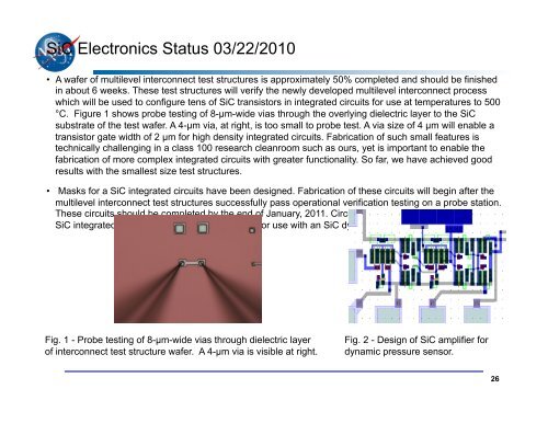
°C. Figure 1 shows probe testing <strong>of</strong> 8-µm-wide vias through the overlying dielectric layer to the SiC<br />
substrate <strong>of</strong> the test wafer. A 4-µm via, at right, is too small to probe test. A via size <strong>of</strong> 4 µm will enable a<br />
transistor gate width <strong>of</strong> 2 µm for high density integrated circuits. Fabrication <strong>of</strong> such small features is<br />
technically challenging in a class 100 research cleanroom such as ours, yet is important to enable the<br />
fabrication <strong>of</strong> more complex integrated circuits with greater functionality. So far, we have achieved good<br />
results with the smallest size test structures.<br />
• Masks for a SiC integrated circuits have been designed. Fabrication <strong>of</strong> these circuits will begin after the<br />
multilevel interconnect test structures successfully pass operational verification testing on a probe station.<br />
These circuits should be completed by the end <strong>of</strong> January, 2011. Circuits to be fabricated include a 500 °C<br />
SiC integrated circuit amplifier (shown in Fig. 2) for use with an SiC dynamic pressure sensor.<br />
Fig. 1 - Probe testing <strong>of</strong> 8-µm-wide vias through dielectric layer<br />
<strong>of</strong> interconnect test structure wafer. A 4-µm via is visible at right.<br />
Fig. 2 - Design <strong>of</strong> SiC amplifier for<br />
dynamic pressure sensor.<br />
26