

Progetto di un capacimetro a microcontrollore per fotodiodi SPAD
Progetto di un capacimetro a microcontrollore per fotodiodi SPAD
Progetto di un capacimetro a microcontrollore per fotodiodi SPAD

You also want an ePaper? Increase the reach of your titles
YUMPU automatically turns print PDFs into web optimized ePapers that Google loves.
CAPITOLO 3. <strong>SPAD</strong>CAPMETER<br />
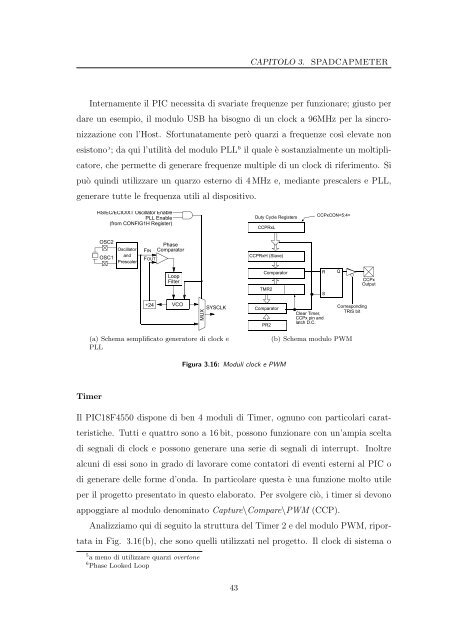
Internamente il PIC necessita <strong>di</strong> svariate frequenze <strong>per</strong> f<strong>un</strong>zionare; giusto <strong>per</strong><br />
dare <strong>un</strong> esempio, il modulo USB ha bisogno <strong>di</strong> <strong>un</strong> clock a 96MHz <strong>per</strong> la sincro-<br />
nizzazione con l’Host. Sfort<strong>un</strong>atamente <strong>per</strong>ò quarzi a frequenze così elevate non<br />
esistono 5 ; da qui l’utilità del modulo PLL 6 il quale è sostanzialmente <strong>un</strong> moltipli-<br />
catore, che <strong>per</strong>mette <strong>di</strong> generare frequenze multiple <strong>di</strong> <strong>un</strong> clock <strong>di</strong> riferimento. Si<br />
può quin<strong>di</strong> utilizzare <strong>un</strong> quarzo esterno <strong>di</strong> 4 MHz e, me<strong>di</strong>ante prescalers e PLL,<br />
generare tutte le frequenza utili al <strong>di</strong>spositivo.<br />
HS/EC/ECIO/XT Oscillator Enable<br />
PLL Enable<br />
(from CONFIG1H Register)<br />
OSC2<br />
OSC1<br />
Oscillator<br />
and<br />
Prescaler<br />
FIN<br />
FOUT<br />
÷24<br />
Phase<br />
Comparator<br />
Loop<br />
Filter<br />
VCO<br />
MUX<br />
SYSCLK<br />
(a) Schema semplificato generatore <strong>di</strong> clock e<br />
PLL<br />
Timer<br />
Duty Cycle Registers<br />
CCPRxL<br />
CCPRxH (Slave)<br />
Comparator<br />
TMR2<br />
Comparator<br />
PR2<br />
Figura 3.16: Moduli clock e PWM<br />
CCPxCON<br />
R<br />
S<br />
Clear Timer,<br />
CCPx pin and<br />
latch D.C.<br />
Q<br />
Correspon<strong>di</strong>ng<br />
TRIS bit<br />
(b) Schema modulo PWM<br />
CCPx<br />
Output<br />
Il PIC18F4550 <strong>di</strong>spone <strong>di</strong> ben 4 moduli <strong>di</strong> Timer, ogn<strong>un</strong>o con particolari carat-<br />
teristiche. Tutti e quattro sono a 16 bit, possono f<strong>un</strong>zionare con <strong>un</strong>’ampia scelta<br />
<strong>di</strong> segnali <strong>di</strong> clock e possono generare <strong>un</strong>a serie <strong>di</strong> segnali <strong>di</strong> interrupt. Inoltre<br />
alc<strong>un</strong>i <strong>di</strong> essi sono in grado <strong>di</strong> lavorare come contatori <strong>di</strong> eventi esterni al PIC o<br />
<strong>di</strong> generare delle forme d’onda. In particolare questa è <strong>un</strong>a f<strong>un</strong>zione molto utile<br />
<strong>per</strong> il progetto presentato in questo elaborato. Per svolgere ciò, i timer si devono<br />
appoggiare al modulo denominato Capture\Compare\PWM (CCP).<br />
Analizziamo qui <strong>di</strong> seguito la struttura del Timer 2 e del modulo PWM, ripor-<br />
tata in Fig. 3.16(b), che sono quelli utilizzati nel progetto. Il clock <strong>di</strong> sistema o<br />
5 a meno <strong>di</strong> utilizzare quarzi overtone<br />
6 Phase Looked Loop<br />
43