pci express 3.0 jitter requirements - Silicon Laboratories Inc.
pci express 3.0 jitter requirements - Silicon Laboratories Inc.
pci express 3.0 jitter requirements - Silicon Laboratories Inc.

Create successful ePaper yourself
Turn your PDF publications into a flip-book with our unique Google optimized e-Paper software.
PCI EXPRESS <strong>3.0</strong> JITTER REQUIREMENTS<br />
1. Introduction<br />
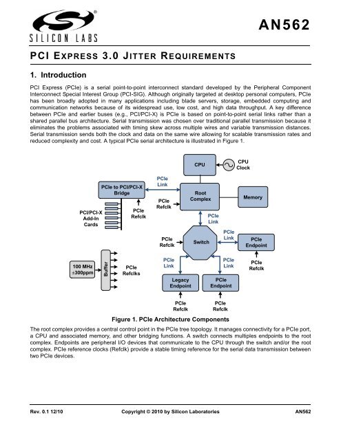
AN562<br />
PCI Express (PCIe) is a serial point-to-point interconnect standard developed by the Peripheral Component<br />
Interconnect Special Interest Group (PCI-SIG). Although originally targeted at desktop personal computers, PCIe<br />
has been broadly adopted in many applications including blade servers, storage, embedded computing and<br />
communication networks because of its widespread use, low cost, and high data throughput. A key difference<br />
between PCIe and earlier buses (e.g., PCI/PCI-X) is PCIe is based on point-to-point serial links rather than a<br />
shared parallel bus architecture. Serial transmission was chosen over traditional parallel transmission because it<br />
eliminates the problems associated with timing skew across multiple wires and variable transmission distances.<br />
Serial transmission sends both the clock and data on the same wire allowing for scalable transmission rates and<br />
reduced complexity and cost. A typical PCIe serial architecture is illustrated in Figure 1.<br />
PCI/PCI-X<br />
Add-In<br />
Cards<br />
100 MHz<br />
±300ppm<br />
PCIe to PCI/PCI-X<br />
Bridge<br />
Buffer<br />
PCIe<br />
Refclk<br />
PCIe<br />
Refclks<br />
PCIe<br />
Link<br />
PCIe<br />
Refclk<br />
PCIe<br />
Refclk<br />
PCIe<br />
Link<br />
Legacy<br />
Endpoint<br />
PCIe<br />
Refclk<br />
Figure 1. PCIe Architecture Components<br />
The root complex provides a central control point in the PCIe tree topology. It manages connectivity for a PCIe port,<br />
a CPU and associated memory, and other bridging functions. A switch connects multiples endpoints to the root<br />
complex. Endpoints are peripheral I/O devices that communicate to the CPU through the switch and/or the root<br />
complex. PCIe reference clocks (Refclk) provide a stable timing reference for the serial data transmission between<br />
two PCIe devices.<br />
Rev. 0.1 12/10 Copyright © 2010 by <strong>Silicon</strong> <strong>Laboratories</strong> AN562<br />
CPU<br />
Root<br />
Complex<br />
Switch<br />
PCIe<br />
Link<br />
PCIe<br />
Link<br />
PCIe<br />
Endpoint<br />
PCIe<br />
Refclk<br />
CPU<br />
Clock<br />
Memory<br />
PCIe<br />
Link PCIe<br />
Endpoint<br />
PCIe<br />
Refclk
AN562<br />
2. PCI Express Link<br />
A PCIe link is made up of one or more lanes which consists of a transmit and receive differential pair. Support for<br />
x1, x2, x4, x8, x12, x16, x32 lanes per link enables a scalable bandwidth to meet the needs of a wide variety of<br />
applications. With the introduction of PCIe 1.0 in 2003, a lane rate of 2.5 GBps was defined, which resulted in a<br />
data throughput of 500 MBps per lane using 8B/10B encoding (2.5 GBps � 10 bits/Byte x 2 directions). In 2007,<br />
PCIe 2.0 doubled the data throughput by increasing the lane rate to 5.0 GBps. PCIe <strong>3.0</strong> released in 2010 once<br />
again doubled the data throughput by increasing the lane rate to 8 GBps and changing to a more efficient<br />
scrambling and encoding scheme (128B/130B). Figure 2 illustrates the flexible data throughput of the PCIe link for<br />
the three PCIe standards.<br />
Number of Lanes per PCIe Link<br />
x1 x2 x4 x8 x12 x16 x32<br />
PCIe 1.1 500 MBps 1 GBps 2 GBps 4 GBps 6 GBps 8 GBps 16 GBps<br />
PCIe 2.1 1 GBps 2 GBps 4 GBps 8 GBps 12 GBps 16 GBps 32 GBps<br />
PCIe <strong>3.0</strong> 2 GBps 4 GBps 8 GBps 16 GBps 24 GBps 32 GBps 64 GBps<br />
Figure 2. PCIe Link and Effective Data Throughput<br />
2 Rev. 0.1<br />
Total Data Throughput per PCIe Link
3. Refclk and Clocking Architectures<br />
AN562<br />
An external clock reference clock (Refclk) is required for transmitting data between two PCIe devices. A Refclk<br />
frequency of 100 MHz ±300 ppm is specified for all line three rates (2.5 GBps, 5.0 GBps, 8.0 GBps). The burden<br />
has been placed on the TX PLL to multiply the 100 MHz Refclk frequency to the desired data rate. Although the<br />
Refclk frequency has remained the same, the <strong>jitter</strong> performance <strong>requirements</strong> of the Refclk have improved to<br />
support the higher data rates prevalent with PCI Express 2.1 and <strong>3.0</strong>. We will look at the Refclk <strong>jitter</strong> <strong>requirements</strong><br />
in the following sections.<br />
The PCIe standards allow for some flexibility in how Refclk is distributed to the PCIe devices in a system. The three<br />
supported clocking architectures are illustrated in Figure 3. The Common Clock RX Architecture is the simplest<br />
and most widely used form of clock distribution between PCIe devices. In this architecture the same 100 MHz<br />
Refclk source is distributed to both the transmitting and receiving PCIe device. In the Data Clocked RX<br />
Architecture, the receiving device does not require a Refclk. Instead it recovers the clock embedded in the<br />
transmitted datastream. The Separate Clocking Architecture uses different clocks for the transmitting and receiving<br />
devices. This is possible because the standard allows up to 600 ppm of frequency separation between the<br />
transmitter and receiver.<br />
Among the deciding factors in selecting the best clocking architecture are system partitioning and Refclk <strong>jitter</strong><br />
performance <strong>requirements</strong>. We will explore these factors in the following sections.<br />
Common Clock Rx Architecture<br />
PCIe<br />
Device A<br />
PCIe<br />
Link<br />
100 MHz<br />
±300ppm<br />
PCIe<br />
Device B<br />
Separate Clock Architecture<br />
PCIe<br />
Device A<br />
100 MHz<br />
±300ppm<br />
PCIe<br />
Link<br />
PCIe<br />
Device B<br />
100 MHz<br />
±300ppm<br />
Figure 3. PCIe Clock Architectures<br />
Data Clocked Rx Architecture<br />
PCIe<br />
Device A<br />
100 MHz<br />
±300ppm<br />
PCIe<br />
Link<br />
PCIe<br />
Device B<br />
Rev. 0.1 3
AN562<br />
4. Refclk Jitter Requirements<br />
Jitter of the reference clock has a direct impact on the efficiency of the data transfer between two PCIe devices.<br />
The data recovery process is able to track a portion of the <strong>jitter</strong> frequencies that are within its bandwidth, but it is<br />
the <strong>jitter</strong> frequencies that it cannot track that must be limited. This untrackable <strong>jitter</strong> spectrum is easily defined using<br />
a series of transfer functions that represent the loop bandwidths of the PLLs and the CDR that affect the data<br />
recovery process. The PCIe standards defines the overall transfer function, parameters (bandwidth and peaking),<br />
and <strong>jitter</strong> limits for each of the three clocking architectures.<br />
4.1. Jitter Requirements for the Common Refclk RX Architecture<br />
Since the reference clock for the Common Clock RX Architecture is distributed to both the transmit and receive<br />
PCIe devices, its overall transfer function, H(s), becomes the difference between the transfer functions of the<br />
transmit path and receive paths. The transfer functions relevant to the PCIe 1.1, 2.1, and <strong>3.0</strong> standards for the<br />
Common Clock RX Architecture are shown in Figure 4.<br />
4 Rev. 0.1
PCIe<br />
Device A<br />
H1(s)<br />
f1_3dB<br />
Tx<br />
Latch<br />
Tx<br />
PLL<br />
PCIe<br />
Link<br />
T1 T2<br />
PCIe<br />
Device B<br />
Rx<br />
Latch<br />
CDR<br />
Rx<br />
PLL<br />
H3(s)<br />
f3_3dB<br />
H2(s)<br />
PCIe 1.1 H( s)<br />
H1( s)<br />
H2( s)<br />
e s � T �<br />
�<br />
� � � �<br />
� H ��<br />
�<br />
3 ( s)<br />
f2_3dB<br />
Overall Jitter Transfer Functions Transfer Function Parameters Defined<br />
PCIe 2.1 H( s)<br />
H1( s)<br />
e s � T �<br />
�� �<br />
� � � H2 ( s)<br />
�<br />
�<br />
PCIe <strong>3.0</strong><br />
100 MHz<br />
±300ppm<br />
where T = 10 ns max<br />
where T = 12 ns max<br />
H( s)<br />
H1( s)<br />
e s � T �<br />
�<br />
� � � H2 ( s)<br />
�<br />
� H ��<br />
� 3 ( s)<br />
H( s)<br />
H2( s)<br />
e s � T �<br />
�<br />
� � � H1 ( s)<br />
�<br />
� H ‘ ��<br />
� 3 ( s)<br />
where T = 12 ns max<br />
f1_3dB<br />
22.0 MHz<br />
f2_3dB<br />
1.5 MHz<br />
f3_3dB<br />
1.5 MHz<br />
f1_3dB<br />
5.0 MHz<br />
f1_3dB<br />
8.0 MHz<br />
f2_3dB<br />
16.0 MHz<br />
f1_3dB<br />
2.0 MHz<br />
f1_3dB<br />
4.0 MHz<br />
f2_3dB<br />
2.0 MHz<br />
f2_3dB<br />
5.0 MHz<br />
f3_3dB<br />
10.0 MHz<br />
PLL and CDR Transfer Functions<br />
2<br />
2�s��1��n1 � �n1 H1 ( s)<br />
s 2<br />
� 2�s��1��n1 �n1 2<br />
��<br />
�<br />
2�s��2��n2 �n2<br />
H2 ( s)<br />
2<br />
�<br />
s 2<br />
��<br />
2<br />
� 2�s��2��n2 � �n2 Refclk Path Delay Difference:<br />
<strong>3.0</strong> dB Peaking<br />
�n1 �� 11.83��2� Mrad/s<br />
�1 �� 0.54<br />
<strong>3.0</strong> dB Peaking<br />
�n2 �� 0.807�� 2 Mrad/s<br />
�2 �� 0.54<br />
1.0 dB Peaking<br />
�n1 �� 1.82�2� Mrad/s<br />
�1 �� 1.16<br />
<strong>3.0</strong> dB Peaking<br />
�n2 �� 8.61�� 2 Mrad/s<br />
�2 �� 0.54<br />
0.01 dB Peaking<br />
�n1 �� 0.448 Mrad/s<br />
�1 �� 14<br />
�n1 �� 0.896Mrad/s<br />
�1 �� 14<br />
0.01 dB Peaking<br />
�n2 �� 0.448 Mrad/s<br />
�2 �� 14<br />
�n2 �� 1.12 Mrad/s<br />
�2 �� 14<br />
<strong>3.0</strong> dB Peaking<br />
Figure 4. Jitter Transfer Functions For The Common Clocked RX Architecture<br />
Tx<br />
PLL<br />
Rx<br />
PLL<br />
CDR<br />
AN562<br />
s<br />
H3( s)<br />
�� �n3 �� 2��� f 3_3dB<br />
s � �n3 T = | T1 – T2 |<br />
�n1 �� 4.31�2� Mrad/s<br />
�1 �� 0.54<br />
2.0 dB Peaking<br />
�n1 �� 6.02 Mrad/s<br />
�1 �� 0.73<br />
�n1 ��12.04 Mrad/s<br />
�1 �� 0.73<br />
1.0 dB Peaking<br />
�n2 �� 4.62 Mrad/s<br />
�2 �� 1.15<br />
�n2 ��11.53 Mrad/s<br />
�2 �� 1.15<br />
Rev. 0.1 5
AN562<br />
Using PCIe 1.1 as an example, the overall transfer function H(s) becomes a bandpass filter as shown in Figure 5.<br />
The area under the curve becomes the untracked <strong>jitter</strong> that needs to be limited to ensure efficient data<br />
transmission.<br />
Gain (dB)<br />
10<br />
0<br />
10<br />
20<br />
30<br />
40<br />
50<br />
60<br />
70<br />
80<br />
90<br />
1 �10 4<br />
100<br />
1 � 10 5<br />
Hs ( ) H1( s)<br />
H2( s)<br />
e s � T �<br />
�<br />
� � � �<br />
� H ��<br />
�<br />
3 ( s)<br />
1 � 10 6<br />
Untracked<br />
Jitter<br />
. Frequency (Hz)<br />
Figure 5. PCIe 1.1 Overall Transfer Function for the Common Clock RX Architecture<br />
As shown in Figure 4 there are two possible TX PLL bandwidths available for PCIe 2.1, so we need to compute the<br />
worst case Refclk <strong>jitter</strong> using the two different bandwidth combination. PCIe <strong>3.0</strong> standard allows even more TX PLL<br />
and RX PLL bandwidth flexibility with 16 different bandwidth combinations and two transfer functions resulting in 32<br />
unique combinations. Again, the resulting worst case <strong>jitter</strong> from these 32 combinations must be below the <strong>jitter</strong><br />
limits specified by the PCIe standards. Refer to the Appendices at the end of this document for a listing all possible<br />
parameter combinations and associated transfer functions.<br />
The Refclk <strong>jitter</strong> limits for all three PCIe standards after the overall transfer function(s) have been applied is shown<br />
in Table 1.<br />
Table 1: Common Refclk RX Architecture Jitter Limits<br />
6 Rev. 0.1<br />
Description Symbol Limit Units<br />
PCIe 1.1 Random Jitter R j 4.7 ps pk-pk<br />
Deterministic Jitter D j 41.9 ps pk-pk<br />
Total Jitter<br />
where Tj = Dj + 14.069 x Rj (for BER 10 -12 )<br />
PCIe 2.1 High Frequency RMS Jitter<br />
Measured from 1.5 MHz to Nyquist (or f REFCLK � 2)<br />
Low Frequency RMS Jitter<br />
Measured from 10 kHz to 1.5 MHz<br />
T j 108 ps pk-pk<br />
J RMS-HF 3.1 ps RMS<br />
J RMS-LF <strong>3.0</strong> ps RMS<br />
PCIe <strong>3.0</strong> Random Jitter J RMS 1.0 ps RMS<br />
Note: All <strong>jitter</strong> measurements are filtered using the overall transfer function(s) defined in Figure 4 after all combinations of<br />
parameters have been exercised. See Appendix A–D.<br />
1 � 10 7<br />
1 � 10 8<br />
f1_3dB: 22.0 MHz , <strong>3.0</strong> dB peaking<br />
f2_3dB: 1.5 MHz , <strong>3.0</strong> dB peaking<br />
f3_3dB: 1.5 MHz
4.2. Jitter Requirements for the Data Clocked RX Architecture<br />
AN562<br />
The Refclk transmission path in a data clock RX architecture is much simpler than in the common clocked RX<br />
architecture since it only has one path. The <strong>jitter</strong> transfer functions for PCIe 2.1 and <strong>3.0</strong> are shown in Figure 6. The<br />
data clocked RX architecture is not defined for PCIe 1.1. Jitter limits are determined using all possible parameter<br />
combinations as outlined in Appendix A. The <strong>jitter</strong> limits for the data clocked RX architecture are shown in Table 2.<br />
H1(s)<br />
f1_3dB<br />
PCIe 1.1<br />
PCIe 2.1 H( s)<br />
��<br />
PCIe <strong>3.0</strong><br />
PCIe<br />
Device A<br />
Tx<br />
Latch<br />
Tx<br />
PLL<br />
100 MHz<br />
±300ppm<br />
PCIe<br />
Link<br />
PCIe<br />
Device B<br />
Rx<br />
Latch<br />
CDR<br />
H3(s)<br />
f3_3dB<br />
PLL and CDR Transfer Functions<br />
2<br />
2�s��1��n1 � �n1 H1 ( s)<br />
s 2<br />
� 2�s��1��n1 �n1 2<br />
��<br />
�<br />
2�s��3��n3 �n3<br />
H3( s)<br />
2<br />
�<br />
s 2<br />
��<br />
2<br />
� 2�s��3��n3 � �n3 Overall Jitter Transfer Functions Transfer Function Parameters<br />
Not defined in PCIe standards<br />
H1 ( s)<br />
� �<br />
Hs ( ) �� H1( s)<br />
� 1 � H3 ( s)<br />
f1_3dB<br />
16.0 MHz<br />
f1_3dB<br />
2.0 MHz<br />
f1_3dB<br />
2.0 MHz<br />
f1_3dB<br />
4.0 MHz<br />
f1_3dB<br />
5.0 MHz<br />
f3_3dB<br />
10 MHz<br />
Figure 6. Jitter Transfer Functions For The Data Clocked RX Architecture<br />
Tx<br />
PLL<br />
CDR<br />
0.5 dB Peaking <strong>3.0</strong> dB Peaking<br />
�n1 �� 8.61�2� Mrad/s<br />
�1 �� 1.75<br />
0.01 dB Peaking<br />
�n1 �� 0.448 Mrad/s<br />
�1 �� 14<br />
2.0 dB Peaking<br />
�n1 �� 6.02 Mrad/s<br />
�1 ��<br />
0.73<br />
�n1 �� 8.61�2� Mrad/s<br />
�1 �� 0.54<br />
0.01 dB Peaking 2.0 dB Peaking<br />
�n1 ��0.896 Mrad/s<br />
�1 �� 14<br />
0.01 dB Peaking 1.0 dB Peaking<br />
�n1 �� 1.12 Mrad/s<br />
�1 �� 14<br />
0.5 dB Peaking 2.0 dB Peaking<br />
�n3 ��16.57 Mrad/s<br />
�3 �� 1.75<br />
1.0 dB Peaking<br />
�n1 �� 4.62 Mrad/s<br />
�1 �� 1.15<br />
�n1 ��12.04 Mrad/s<br />
�1 �� 0.73<br />
�n1 ��11.53 Mrad/s<br />
�1 �� 1.15<br />
�n3 �� 33.8 Mrad/s<br />
�3 �� 0.73<br />
Rev. 0.1 7
AN562<br />
Table 2: Data Refclk RX Architecture Jitter Limits<br />
PCIe 1.1 Not defined in PCIe standards<br />
PCIe 2.1 High Frequency RMS Jitter<br />
Measured from 1.5 MHz to Nyquist (or f REFCLK � 2)<br />
Low Frequency RMS Jitter<br />
Measured from 10 kHz to 1.5 MHz<br />
4.3. Jitter Requirements for the Separate Clock Architecture<br />
The separate clock architecture uses two independent reference clocks for the transmitting and receiving PCIe<br />
devices as shown in Figure 7. Using two separate Refclks of 100 MHz ±300 ppm is possible because the PCIe<br />
standards allow for up to 600 ppm frequency separation between clocks. The consequence of using the entire<br />
frequency margin is that spread spectrum must be turned off for both Refclk sources.<br />
Figure 7. Separate Clock Architecture<br />
There is no overall <strong>jitter</strong> transfer function defined in the PCIe standards for this architecture. Since both Refclks are<br />
independent, their phase <strong>jitter</strong> is passed through the TX and RX PLLs independently and a maximum PLL<br />
bandwidth of 16 MHz with <strong>3.0</strong> dB of peaking should be assumed. Since both Refclks are independent, the random<br />
<strong>jitter</strong> components of each clock are added as a root sum square (RSS).<br />
The PCIe standards do not specify <strong>jitter</strong> limits for this clock architecture, although it states that <strong>jitter</strong> must be<br />
considerably tighter than for the other two architectures. Ultimately the <strong>jitter</strong> limits will depend on the TX and RX<br />
PCIe device specifications.<br />
8 Rev. 0.1<br />
Description Symbol Limit Units<br />
J RMS-HF 4.0 ps RMS<br />
J RMS-LF 7.5 ps RMS<br />
PCIe <strong>3.0</strong> Random Jitter J RMS 1.0 ps RMS<br />
Note: All <strong>jitter</strong> measurements are filtered using the overall transfer function(s) defined in Figure 4 after all combinations of<br />
parameters have been exercised. See Appendix A.<br />
PCIe<br />
Device A<br />
H1(s)<br />
f1_3dB<br />
Tx<br />
Latch<br />
Tx<br />
PLL<br />
100 MHz<br />
±300ppm<br />
PCIe<br />
Link<br />
� � 2<br />
Xs ( ) �� X1( s)<br />
�H<br />
1( s)<br />
PCIe<br />
Device B<br />
Rx<br />
Latch<br />
CDR<br />
Rx<br />
PLL<br />
100 MHz<br />
±300ppm<br />
�X2( s)<br />
�H<br />
2( s)<br />
� 2<br />
�<br />
H2(s)<br />
f2_3dB<br />
2<br />
2�s��1��n1 � �n1 H1 ( s)<br />
s 2<br />
��<br />
2<br />
� 2�s��1��n1 � �n1 2�s��2��n2 �n2<br />
H2 ( s)<br />
2<br />
�<br />
s 2<br />
��<br />
2<br />
� 2�s��2��n2 � �n2 f1_3dB<br />
16.0 MHz<br />
f2_3dB<br />
16.0 MHz<br />
<strong>3.0</strong> dB Peaking<br />
�n1 �� 8.61� 2� Mrad/s<br />
�1 �� 0.54<br />
<strong>3.0</strong> dB Peaking<br />
�n2 �� 8.61�2� Mrad/s<br />
�2 �� 0.54<br />
where, X( s)<br />
– Total Jitter<br />
X 1( s)<br />
– Tx Refclk Jitter<br />
X 2( s)<br />
– Rx Refclk Jitter
5. Spread Spectrum Clocking (SSC)<br />
AN562<br />
Spread spectrum clocking is a technique used to lower the amount of radiated electromagnetic interference (EMI)<br />
that is generated from high speed digital signals. Spread spectrum clocks use low frequency modulation of the<br />
carrier frequency to spread out the radiated energy across a broader range of frequencies. The frequency<br />
spectrum of a clock with and without spread spectrum is illustrated in Figure 8. Radiation from data lines<br />
transmitted with a device using a spread spectrum clock reference will also benefit from the same EMI reduction.<br />
Reduced<br />
Amplitude and<br />
EMI<br />
Clock with<br />
SSC On<br />
(downspread)<br />
Carrier Frequency<br />
Clock with<br />
SSC Off<br />
Figure 8. Spectrum Analyzer Plot of a Clock With and Without Spread Spectrum<br />
PCIe devices are specified to reliably transmit data when using a Refclk with a spread spectrum modulation rate of<br />
30–33 kHz and modulation amplitude of 0 to –0.5% (i.e., downspread 0.5% in reference to the carrier frequency).<br />
Because each PCIe device must transmit within a bit rate of ±300 ppm of each other, the same Refclk must be<br />
supplied to both devices if SSC is used. The separate clocking architecture will therefore not work if SSC is turned<br />
on unless both clocks are synchronized to a common source. The bandwidth of such a synchronizing clock (i.e., a<br />
phase-locked loop) must be high enough to track the 30–33 kHz modulation rate. For practical purposes, this<br />
means a clock generator must have a loop bandwidth greater than 1.5 MHz to ensure the SSC clock is tracked.<br />
Using SSC is possible for the Common Clocked RX Architecture and Data Clocked RX Architecture since they use<br />
a single Refclk.<br />
f<br />
Rev. 0.1 9
AN562<br />
6. HCSL Output Signal Format<br />
The host clock signal level (HCSL) is the output signal format specified by the PCI Express Card<br />
Electromechanical Specification 2.0 for the Refclk signal and it is commonly found in the PC and Server markets.<br />
Using a standardized signalling level for Refclk ensures compatibility between PC motherboards and add-in cards<br />
manufactured by different vendors.<br />
HCSL is a differential current mode signal that nominally swings from 0 V to 700 mV. HCSL is a point-to-point<br />
signal format meaning that a separate output driver is required to drive each PCIe device. Multidrop connections<br />
(one output driver to multiple devices) are not supported. HCSL drivers are source terminated as shown in<br />
Figure 9.<br />
Refclk<br />
PCI Express<br />
Clock Driver<br />
22-33�<br />
22-33�<br />
50 �<br />
Keep very<br />
close to driver<br />
50 �<br />
Figure 9. HCSL Output Driver Termination<br />
Systems that don’t require compatibility with PCIe add-in cards or PCIe functions implemented in FPGAs can use<br />
other Refclk signal formats. LVDS, LVPECL, and even LVCMOS are common.<br />
10 Rev. 0.1<br />
50 �<br />
50 �<br />
PCIe<br />
Connector<br />
PCI Express<br />
Add-In Card<br />
Refclk
7. A Typical PCI Express Application<br />
AN562<br />
<strong>Silicon</strong> Labs offers a variety of clock devices that allows for flexible PCIe Refclk distribution. For example, the<br />
Si5338 I 2 C Programmable Any-Frequency, Any-Output Quad Clock Generator is an ideal device for generating<br />
PCIe clocks:<br />
� Compliant with PCI Express <strong>3.0</strong> and legacy standards (2.1, 1.1)<br />
� PCI Express <strong>3.0</strong> <strong>jitter</strong> = 0.12 ps RMS (10x lower than the requirement)<br />
� Generates up to four 100 MHz HCSL output clocks but is programmable with other frequencies and signal<br />
formats. This allows one clock device to generate PCIe Refclks and other board clocks of different frequencies<br />
and signal formats.<br />
� Output frequencies are programmable per output from 5 MHz to 710 MHz.<br />
� Independent VDDO for each output clock enables integrated level translation.<br />
� Output signal formats are programmable per output as HCSL, LVDS, LVPECL or LVCMOS.<br />
� Excellent <strong>jitter</strong> performance allows Refclk generation for Common Refclk RX, Data Clocked RX, and Separate<br />
Clock Architectures.<br />
� Spread spectrum can be enabled or disabled per output with programmable modulation rate and modulation<br />
amplitude per output.<br />
� Built-in HCSL terminations.<br />
� Small 4x4 mm package<br />
A typical use of the Si5338 in a PCIe application is shown in Figure 10. In this example the Si5338 replaces a<br />
100 MHz clock oscillator with spread spectrum, a 1:2 HCSL buffer, a 66.6667 MHz clock oscillator, and a 125 MHz<br />
clock oscillator.<br />
Motherboard<br />
25 MHz<br />
XTAL<br />
+/- 100ppm<br />
Si5338 Quad Clock Generator<br />
OSC<br />
PLL<br />
Multi-<br />
Synth 0<br />
Multi-<br />
Synth 1<br />
Multi-<br />
Synth 2<br />
Multi-<br />
Synth 3<br />
CPU<br />
66.66 MHz<br />
LVCMOS<br />
100 MHz HCSL<br />
100 MHz HCSL<br />
Ethernet<br />
125 MHz<br />
LVCMOS<br />
PCIe<br />
Device<br />
Add-In Board<br />
PCIe<br />
Device<br />
Figure 10. PCIe Application Using the Si5338 as the Refclk Generator<br />
Rev. 0.1 11
AN562<br />
8. Conclusion<br />
There are several things to consider when choosing the right reference clock for a PCI Express application. Jitter<br />
performance is a key consideration for ensuring efficient and reliable data transfer between two PCIe devices. This<br />
can only be guaranteed by choosing a device that specifies <strong>jitter</strong> across all PLL and CDR bandwidths and clocking<br />
architecture transfer functions. A clock with selectable spread spectrum can also be an important consideration for<br />
meeting EMI <strong>requirements</strong>. In some cases PCIe clocks need flexible output signal formats and frequencies other<br />
than the standard 100 MHz HCSL signal format. A clock generator like the Si5338 provides the reliability and<br />
flexibility needed to meet all PCI Express applications and <strong>requirements</strong>.<br />
9. References<br />
� PCI Express Base Specification Revision 1.1, March 28, 2005.<br />
� PCI Express Jitter and BER Revision 1.0, February, 2005.<br />
� PCI Express Card Electromechanical Specification Revision 2.0, April 11, 2007.<br />
� PCI Express Base Specification Revision 2.1, March 4, 2009.<br />
� PCI Express Base Specification Revision <strong>3.0</strong>, November 10, 2010.<br />
� <strong>Silicon</strong> Labs Si5338 I 2 C Programmable Any-Frequency, Any-Output Quad Clock Generator data sheet.<br />
12 Rev. 0.1
AN562<br />
APPENDIX A—PCIE JITTER PARAMETERS AND LIMITS<br />
Table 3 lists all bandwidth combinations for all three clock architecture defined by the PCIe standards. Jitter<br />
performance of the Si5338/Si5334 are listed for comparison.<br />
Table 3. PCIe Jitter Transfer Function Parameters and Jitter Limits<br />
# Parameters Jitter Limits<br />
PCIe 1.1 1 22 MHz/<br />
<strong>3.0</strong> dB<br />
PCIe 2.1 1 5.0 MHz/<br />
1.0 dB<br />
f1_3dB /peak f2_3dB /peak f3_3dB /peak T Symbol PCIe<br />
Rqmt<br />
Common Clocked RX Architecture<br />
2 8.0 MHz/<br />
<strong>3.0</strong> dB<br />
Si5338/34<br />
Measured<br />
Units<br />
1.5MHz/ <strong>3.0</strong>dB 1.5MHz 10ns Rj 4.7 — ps<br />
RMS<br />
Dj 41.9 — ps pkpk<br />
Tj 108 11.2 ps pkpk<br />
16.0 MHz/ <strong>3.0</strong> dB No CDR BW/<br />
Peak specified<br />
12 ns J RMS-HF 3.1 0.49 ps<br />
RMS<br />
J RMS-LF <strong>3.0</strong> 0.25<br />
16.0MHz/ <strong>3.0</strong>dB JRMS-HF 3.1 0.49<br />
JRMS-LF <strong>3.0</strong> 0.21<br />
Rev. 0.1 13
AN562<br />
Table 3. PCIe Jitter Transfer Function Parameters and Jitter Limits<br />
# Parameters Jitter Limits<br />
f 1_3dB /peak f 2_3dB /peak f 3_3dB /peak T Symbol PCIe<br />
Rqmt<br />
PCIe <strong>3.0</strong> 1<br />
2<br />
2.0 MHz/<br />
0.01 dB<br />
2.0 MHz/ 0.01 dB<br />
2.0 MHz/1.0 dB<br />
10 MHz/Peak<br />
not specified<br />
12 ns JRMS 1.0<br />
1.0<br />
0.04<br />
0.03<br />
ps<br />
RMS<br />
3 5.0 MHz/0.01 dB 1.0 0.12<br />
4 5.0 MHz/1.0 dB 1.0 0.11<br />
5 2.0 MHz/ 2.0 MHz/0.01 dB 1.0 0.06<br />
6 2.0 dB 2.0 MHz/1.0 dB 1.0 0.05<br />
7 5.0 MHz/0.01 dB 1.0 0.14<br />
8 5.0 MHz/1.0 dB 1.0 0.14<br />
9 4.0 MHz/ 2.0 MHz/0.01 dB 1.0 0.07<br />
10 0.01 dB 2.0 MHz/1.0 dB 1.0 0.08<br />
11 5.0 MHz/0.01 dB 1.0 0.09<br />
12 5.0 MHz/1.0 dB 1.0 0.08<br />
13 4.0 MHz/ 2.0 MHz/0.01 dB 1.0 0.08<br />
14 2.0 dB 2.0 MHz/1.0 dB 1.0 0.08<br />
15 5.0 MHz/0.01 dB 1.0 0.12<br />
16 5.0 MHz/1.0 dB 1.0 0.10<br />
1’<br />
2’<br />
2.0 MHz/<br />
0.01 dB<br />
2.0MHz/0.01dB<br />
2.0 MHz/1.0 dB<br />
10MHz/Peak<br />
not specified<br />
12 ns JRMS 1.0<br />
1.0<br />
0.04<br />
0.05<br />
ps<br />
RMS<br />
3’ 5.0 MHz/0.01 dB 1.0 0.09<br />
4’ 5.0 MHz/1.0 dB 1.0 0.09<br />
5’ 2.0 MHz/ 2.0 MHz/0.01 dB 1.0 0.05<br />
6’ 2.0 dB 2.0 MHz/1.0 dB 1.0 0.04<br />
7’ 5.0 MHz/0.01 dB 1.0 0.12<br />
8’ 5.0 MHz/1.0 dB 1.0 0.12<br />
9’ 4.0 MHz/ 2.0 MHz/0.01 dB 1.0 0.09<br />
10’ 0.01 dB 2.0 MHz/1.0 dB 1.0 0.10<br />
11’ 5.0 MHz/0.01 dB 1.0 0.08<br />
12’ 5.0 MHz/1.0 dB 1.0 0.09<br />
13’ 4.0 MHz/ 2.0 MHz/0.01 dB 1.0 0.08<br />
14’ 2.0 dB 2.0 MHz/1.0 dB 1.0 0.09<br />
15’ 5.0 MHz/0.01 dB 1.0 0.12<br />
16’ 5.0 MHz/1.0 dB 1.0 0.07<br />
14 Rev. 0.1<br />
Si5338/34<br />
Measured<br />
Units
Table 3. PCIe Jitter Transfer Function Parameters and Jitter Limits<br />
AN562<br />
# Parameters Jitter Limits<br />
f1_3dB /peak f2_3dB /peak f3_3dB /peak T Symbol PCIe<br />
Rqmt<br />
Si5338/34<br />
Measured<br />
Units<br />
PCIe 1.1<br />
Data Clocked RX Architecture<br />
Not specified in PCIe standards<br />
PCIe 2.1 1 16.0 MHz/<br />
0.5 dB<br />
N/A N/A N/A JRMS-HF JRMS-LF 4.0<br />
7.5<br />
0.65<br />
0.79<br />
ps<br />
RMS<br />
2 16.0 MHz/<br />
<strong>3.0</strong> dB<br />
JRMS-HF JRMS-LF 4.0<br />
7.5<br />
0.62<br />
0.784<br />
ps<br />
RMS<br />
PCIe <strong>3.0</strong> 1 2.0 MHz/<br />
0.01 dB<br />
N/A 10 MHz/<br />
0.5 dB<br />
N/A JRMS 1.0 0.10 ps<br />
RMS<br />
2 2.0 MHz/<br />
1.0 dB<br />
0.10<br />
3 2.0 MHz/<br />
2.0 dB<br />
0.10<br />
4 4.0 MHz/<br />
0.01 dB<br />
0.14<br />
5 4.0 MHz/<br />
2.0 dB<br />
0.15<br />
6 5.0 MHz/<br />
0.5 dB<br />
0.16<br />
7 5.0 MHz/<br />
2.0 dB<br />
0.17<br />
8 2.0 MHz/<br />
10 MHz/<br />
0.09<br />
0.01 dB<br />
2.0 dB<br />
9 2.0 MHz/<br />
1.0 dB<br />
0.08<br />
10 2.0 MHz/<br />
2.0 dB<br />
0.07<br />
11 4.0 MHz/<br />
0.01 dB<br />
0.15<br />
12 4.0 MHz/<br />
2.0 dB<br />
0.14<br />
13 5.0 MHz/<br />
0.5 dB<br />
0.17<br />
14 5.0 MHz/<br />
2.0 dB<br />
0.16<br />
PCIe 1.1<br />
Separate Clock Architecture<br />
Not specified in PCIe standards<br />
PCIe 2.1<br />
PCIe <strong>3.0</strong><br />
1<br />
1<br />
16.0 MHz/<br />
<strong>3.0</strong> dB<br />
16.0 MHz/<strong>3.0</strong> dB N/A N/A JRMS No<br />
Spec<br />
—<br />
—<br />
ps<br />
RMS<br />
Rev. 0.1 15
AN562<br />
APPENDIX B—COMMON CLOCK RX ARCHITECTURE<br />
OVERALL TRANSFER FUNCTIONS<br />
Gain (dB)<br />
log� H�sk� �<br />
� Hs � k�<br />
�<br />
� � � �<br />
Gain (dB)<br />
H 1 s k<br />
10<br />
0<br />
10<br />
20<br />
30<br />
40<br />
50<br />
60<br />
70<br />
80<br />
90<br />
1 �10 4<br />
100<br />
10<br />
0<br />
10<br />
20<br />
30<br />
40<br />
50<br />
60<br />
70<br />
80<br />
90<br />
1 �10 4<br />
100<br />
PCIe 1.1 H() s H1() s H2()e s<br />
s � T �<br />
���<br />
� � � �<br />
��H3() s<br />
1 � 10 5<br />
1 �10 5<br />
1 �10 6<br />
fk f (Hz)<br />
Frequency (Hz)<br />
1 �10 6<br />
fk f (Hz)<br />
Frequency (Hz)<br />
1 � 10 7<br />
PCIe 2.1 H() s H1()e s<br />
s � T �<br />
���<br />
� � �H2<br />
() s �<br />
�<br />
1 �10 7<br />
16 Rev. 0.1<br />
.<br />
.<br />
1 � 10 8<br />
1 �10 8<br />
f1_3dB = 22.0 MHz @ <strong>3.0</strong> dB peaking<br />
f2_3dB = 1.5 MHz @ <strong>3.0</strong> dB peaking<br />
f3_3dB = 1.5 MHz, T = 10 ns<br />
f1_3dB = 5.0 MHz @ 1.0 dB peaking<br />
f2_3dB = 16.0 MHz @ <strong>3.0</strong> dB peaking<br />
T = 12 ns<br />
f1_3dB = 8.0 MHz @ <strong>3.0</strong>dB peaking<br />
f2_3dB = 16.0 MHz @ <strong>3.0</strong>dB peaking<br />
T = 12 ns
g� Ha�sk� �<br />
g� Hb�sk� �<br />
Gain (dB)<br />
� � � �<br />
g H c s k<br />
� � � �<br />
g H d s k<br />
� Ha�sk� �<br />
� Hb�sk� �<br />
Gain (dB)<br />
� � � �<br />
H c s k<br />
� Hd�sk� �<br />
g� Ha�sk� �<br />
g� Hb�sk� �<br />
Gain (dB)<br />
� � � �<br />
g H c s k<br />
� � � �<br />
g H d s k<br />
10<br />
10<br />
0<br />
10<br />
20<br />
30<br />
40<br />
50<br />
60<br />
70<br />
80<br />
90<br />
0<br />
10<br />
20<br />
30<br />
40<br />
50<br />
60<br />
70<br />
80<br />
90<br />
1 �10 4<br />
100<br />
1 �10 4<br />
100<br />
10<br />
0<br />
10<br />
20<br />
30<br />
40<br />
50<br />
60<br />
70<br />
80<br />
90<br />
1 �10 4<br />
100<br />
PCIe <strong>3.0</strong> Hs () H1()e s<br />
s � T �<br />
���<br />
� � �H2()<br />
s �<br />
� �H3()<br />
s<br />
1 �10 5<br />
PCIe <strong>3.0</strong> Hs () H1()e s<br />
s � T �<br />
���<br />
� � �H2()<br />
s �<br />
� �H3()<br />
s<br />
1 �10 5<br />
1 �10 5<br />
1 �10 6<br />
fk f (Hz)<br />
Frequency (Hz)<br />
1 �10 6<br />
fk f (Hz)<br />
Frequency (Hz)<br />
1 �10 6<br />
fk f (Hz)<br />
1 �10 7<br />
PCIe <strong>3.0</strong> Hs () H1()e s<br />
s � T �<br />
���<br />
� � �H2()<br />
s �<br />
� �H3()<br />
s<br />
Frequency (Hz)<br />
.<br />
1 �10 7<br />
.<br />
1 �10 7<br />
1 �10 8<br />
1 �10 8<br />
1 �10 8<br />
AN562<br />
f1_3dB = 2.0 MHz @ 0.01 dB peaking<br />
f2_3dB = 2.0 MHz @ 1.0 dB peaking<br />
f3_3dB = 10.0 MHz, T = 12 ns<br />
f1_3dB = 2.0 MHz @ 0.01 dB peaking<br />
f2_3dB = 2.0 MHz @ 1.0 dB peaking<br />
f3_3dB = 10.0 MHz, T = 12 ns<br />
f1_3dB = 2.0 MHz @ 0.01 dB peaking<br />
f2_3dB = 5.0 MHz @ 0.01 dB peaking<br />
f3_3dB = 10.0 MHz, T = 12 ns<br />
f1_3dB = 2.0 MHz @ 0.01 dB peaking<br />
f2_3dB = 5.0 MHz @ 1.0 dB peaking<br />
f3_3dB = 10.0 MHz, T = 12 ns<br />
f1_3dB = 2.0 MHz @ 2.0 dB peaking<br />
f2_3dB = 2.0 MHz @ 1.0 dB peaking<br />
f3_3dB = 10.0 MHz, T = 12 ns<br />
f1_3dB = 2.0 MHz @ 2.0 dB peaking<br />
f2_3dB = 2.0 MHz @ 1.0 dB peaking<br />
f3_3dB = 10.0 MHz, T = 12 ns<br />
f1_3dB = 2.0 MHz @ 2.0 dB peaking<br />
f2_3dB = 5.0 MHz @ 0.01 dB peaking<br />
f3_3dB = 10.0 MHz, T = 12 ns<br />
f1_3dB = 2.0 MHz @ 2.0 dB peaking<br />
f2_3dB = 5.0 MHz @ 1.0 dB peaking<br />
f3_3dB = 10.0 MHz, T = 12 ns<br />
f1_3dB = 4.0 MHz @ 0.01 dB peaking<br />
f2_3dB = 2.0 MHz @ 1.0 dB peaking<br />
f3_3dB = 10.0 MHz, T = 12 ns<br />
f1_3dB = 4.0 MHz @ 0.01 dB peaking<br />
f2_3dB = 2.0 MHz @ 1.0 dB peaking<br />
f3_3dB = 10.0 MHz, T = 12 ns<br />
f1_3dB = 4.0 MHz @ 0.01 dB peaking<br />
f2_3dB = 5.0 MHz @ 0.01 dB peaking<br />
f3_3dB = 10.0 MHz, T = 12 ns<br />
f1_3dB = 4.0 MHz @ 0.01 dB peaking<br />
f2_3dB = 5.0 MHz @ 1.0 dB peaking<br />
f3_3dB = 10.0 MHz, T = 12 ns<br />
Rev. 0.1 17
AN562<br />
� Ha�sk� �<br />
� Hb�sk� �<br />
Gain (dB)<br />
� Hc�sk� �<br />
� � � �<br />
H d s k<br />
Hap�sk� �<br />
Hbp�sk� �<br />
Gain (dB)<br />
� � �<br />
H cp s k<br />
� � �<br />
H dp s k<br />
Hap�sk� �<br />
Hbp�sk� �<br />
Gain (dB)<br />
� � �<br />
H cp s k<br />
� � �<br />
H dp s k<br />
10<br />
0<br />
10<br />
20<br />
30<br />
40<br />
50<br />
60<br />
70<br />
80<br />
90<br />
1 �10 4<br />
100<br />
10<br />
0<br />
10<br />
20<br />
30<br />
40<br />
50<br />
60<br />
70<br />
80<br />
90<br />
1 �10 4<br />
100<br />
10<br />
0<br />
10<br />
20<br />
30<br />
40<br />
50<br />
60<br />
70<br />
80<br />
90<br />
1 �10 4<br />
100<br />
PCIe <strong>3.0</strong> Hs () H1()e s<br />
s � T �<br />
���<br />
� � �H2()<br />
s �<br />
� �H3()<br />
s<br />
1 �10 5<br />
PCIe <strong>3.0</strong> Hs () H2()e s<br />
s<br />
‘ � � T�<br />
��� � � H1( s)<br />
�<br />
� �H3()<br />
s<br />
1 �10 5<br />
1 � 10 5<br />
1 �10 6<br />
fk f (Hz)<br />
Frequency (Hz)<br />
1 �10 6<br />
fk f (Hz)<br />
Frequency (Hz)<br />
1 �10 6<br />
fk f (Hz)<br />
Frequency (Hz)<br />
1 �10 7<br />
PCIe <strong>3.0</strong> Hs () H2()e s<br />
s<br />
‘ � � T�<br />
��� � � H1( s)<br />
�<br />
� �H3()<br />
s<br />
18 Rev. 0.1<br />
.<br />
1 �10 7<br />
.<br />
1 � 10 7<br />
1 �10 8<br />
1 �10 8<br />
1 � 10 8<br />
f1_3dB = 4.0 MHz @ 2.0 dB peaking<br />
f2_3dB = 2.0 MHz @ 1.0 dB peaking<br />
f3_3dB = 10.0 MHz, T = 12 ns<br />
f1_3dB = 4.0 MHz @ 2.0 dB peaking<br />
f2_3dB = 2.0 MHz @ 1.0 dB peaking<br />
f3_3dB = 10.0 MHz, T = 12 ns<br />
f1_3dB = 4.0 MHz @ 2.0 dB peaking<br />
f2_3dB = 5.0 MHz @ 0.01 dB peaking<br />
f3_3dB = 10.0 MHz, T = 12 ns<br />
f1_3dB = 4.0 MHz @ 2.0 dB peaking<br />
f2_3dB = 5.0 MHz @ 1.0 dB peaking<br />
f3_3dB = 10.0 MHz, T = 12 ns<br />
f1_3dB = 2.0 MHz @ 0.01 dB peaking<br />
f2_3dB = 2.0 MHz @ 1.0 dB peaking<br />
f3_3dB = 10.0 MHz, T = 12 ns<br />
f1_3dB = 2.0 MHz @ 0.01 dB peaking<br />
f2_3dB = 2.0 MHz @ 1.0 dB peaking<br />
f3_3dB = 10.0 MHz, T = 12 ns<br />
f1_3dB = 2.0 MHz @ 0.01 dB peaking<br />
f2_3dB = 5.0 MHz @ 0.01 dB peaking<br />
f3_3dB = 10.0 MHz, T = 12 ns<br />
f1_3dB = 2.0 MHz @ 0.01 dB peaking<br />
f2_3dB = 5.0 MHz @ 1.0 dB peaking<br />
f3_3dB = 10.0 MHz, T = 12 ns<br />
f1_3dB = 2.0 MHz @ 2.0 dB peaking<br />
f2_3dB = 2.0 MHz @ 1.0 dB peaking<br />
f3_3dB = 10.0 MHz, T = 12 ns<br />
f1_3dB = 2.0 MHz @ 2.0 dB peaking<br />
f2_3dB = 2.0 MHz @ 1.0 dB peaking<br />
f3_3dB = 10.0 MHz, T = 12 ns<br />
f1_3dB = 2.0 MHz @ 2.0 dB peaking<br />
f2_3dB = 5.0 MHz @ 0.01 dB peaking<br />
f3_3dB = 10.0 MHz, T = 12 ns<br />
f1_3dB = 2.0 MHz @ 2.0 dB peaking<br />
f2_3dB = 5.0 MHz @ 1.0 dB peaking<br />
f3_3dB = 10.0 MHz, T = 12 ns
Hap�sk� �<br />
Hbp�sk� �<br />
Gain (dB)<br />
� � �<br />
H cp s k<br />
� � �<br />
H dp s k<br />
Hap�sk� �<br />
Hbp�sk� �<br />
Gain (dB)<br />
� � �<br />
H cp s k<br />
� � �<br />
H dp s k<br />
10<br />
0<br />
10<br />
20<br />
30<br />
40<br />
50<br />
60<br />
70<br />
80<br />
90<br />
1 �10 4<br />
100<br />
10<br />
0<br />
10<br />
20<br />
30<br />
40<br />
50<br />
60<br />
70<br />
80<br />
90<br />
1 �10 4<br />
100<br />
PCIe <strong>3.0</strong> Hs () H2()e s<br />
s<br />
‘<br />
� � T�<br />
��� � � H1( s)<br />
�<br />
� �H3()<br />
s<br />
1 �10 5<br />
PCIe <strong>3.0</strong> Hs () H2()e s<br />
s<br />
‘ � � T�<br />
��� � � H1( s)<br />
�<br />
� �H3()<br />
s<br />
1 �10 5<br />
1 �10 6<br />
fk f (Hz)<br />
Frequency (Hz)<br />
1 �10 6<br />
fk f (Hz)<br />
Frequency (Hz)<br />
.<br />
.<br />
1 �10 7<br />
1 �10 7<br />
1 �10 8<br />
1 �10 8<br />
AN562<br />
f1_3dB = 4.0 MHz @ 0.01 dB peaking<br />
f2_3dB = 2.0 MHz @ 1.0 dB peaking<br />
f3_3dB = 10.0 MHz, T = 12 ns<br />
f1_3dB = 4.0 MHz @ 0.01 dB peaking<br />
f2_3dB = 2.0 MHz @ 1.0 dB peaking<br />
f3_3dB = 10.0 MHz, T = 12 ns<br />
f1_3dB = 4.0 MHz @ 0.01 dB peaking<br />
f2_3dB = 5.0 MHz @ 0.01 dB peaking<br />
f3_3dB = 10.0 MHz, T = 12 ns<br />
f1_3dB = 4.0 MHz @ 0.01 dB peaking<br />
f2_3dB = 5.0 MHz @ 1.0 dB peaking<br />
f3_3dB = 10.0 MHz, T = 12 ns<br />
f1_3dB = 4.0 MHz @ 2.0 dB peaking<br />
f2_3dB = 2.0 MHz @ 1.0 dB peaking<br />
f3_3dB = 10.0 MHz, T = 12 ns<br />
f1_3dB = 4.0 MHz @ 2.0 dB peaking<br />
f2_3dB = 2.0 MHz @ 1.0 dB peaking<br />
f3_3dB = 10.0 MHz, T = 12 ns<br />
f1_3dB = 4.0 MHz @ 2.0 dB peaking<br />
f2_3dB = 5.0 MHz @ 0.01 dB peaking<br />
f3_3dB = 10.0 MHz, T = 12 ns<br />
f1_3dB = 4.0 MHz @ 2.0 dB peaking<br />
f2_3dB = 5.0 MHz @ 1.0 dB peaking<br />
f3_3dB = 10.0 MHz, T = 12 ns<br />
Rev. 0.1 19
AN562<br />
APPENDIX C—DATA CLOCKED RX ARCHITECTURE<br />
OVERALL TRANSFER FUNCTIONS<br />
H1�sk� �<br />
� � �<br />
Gain (dB)<br />
H 2 s k<br />
Ha�sk� �<br />
Hb�sk� �<br />
� � �<br />
Gain (dB)<br />
H c s k<br />
10<br />
0<br />
10<br />
20<br />
30<br />
40<br />
50<br />
60<br />
70<br />
80<br />
90<br />
1 �10 4<br />
100<br />
10<br />
0<br />
10<br />
20<br />
30<br />
40<br />
50<br />
60<br />
70<br />
80<br />
90<br />
1 �10 4<br />
100<br />
1 � 10 5<br />
1 �10 5<br />
PCIe 2.1 Hs ()�� H1() s<br />
1 �10 6<br />
fk f (Hz)<br />
Frequency (Hz)<br />
1 �10 6<br />
fk f (Hz)<br />
1 � 10 7<br />
PCIe <strong>3.0</strong> Hs () ��H1s<br />
() ��1�H3()<br />
s �<br />
Frequency (Hz)<br />
1 �10 7<br />
20 Rev. 0.1<br />
.<br />
.<br />
1 � 10 8<br />
1 �10 8<br />
f1_3dB = 16.0 MHz @ 0.5 dB peaking<br />
f1_3dB = 16.0 MHz @ <strong>3.0</strong> dB peaking<br />
f1_3dB = 2.0 MHz @ 0.01 dB peaking<br />
f3_3dB = 10.0 MHz @ 0.5 dB peaking<br />
f1_3dB = 2.0 MHz @ 1.0 dB peaking<br />
f3_3dB = 10.0 MHz @ 0.5 dB peaking<br />
f1_3dB = 2.0 MHz @ 2.0 dB peaking<br />
f3_3dB = 10.0 MHz @ 0.5 dB peaking
Ha2�sk� �<br />
Hb2�sk� �<br />
Gain (dB)<br />
� � �<br />
H c2 s k<br />
Ha�sk� �<br />
Hb�sk� �<br />
Gain (dB)<br />
� � �<br />
H a2 s k<br />
� � �<br />
H b2 s k<br />
Ha�sk� �<br />
Hb�sk� �<br />
Gain (dB)<br />
� � �<br />
H a2 s k<br />
� � �<br />
H b2 s k<br />
10<br />
0<br />
10<br />
20<br />
30<br />
40<br />
50<br />
60<br />
70<br />
80<br />
90<br />
1 �10 4<br />
100<br />
10<br />
0<br />
10<br />
20<br />
30<br />
40<br />
50<br />
60<br />
70<br />
80<br />
90<br />
1 �10 4<br />
100<br />
10<br />
0<br />
10<br />
20<br />
30<br />
40<br />
50<br />
60<br />
70<br />
80<br />
90<br />
1 �10 4<br />
100<br />
PCIe <strong>3.0</strong> Hs () ��H1s<br />
() ��1�H3()<br />
s �<br />
1 �10 5<br />
1 � 10 5<br />
1 �10 6<br />
fk f (Hz)<br />
Frequency (Hz)<br />
1 �10 6<br />
fk f (Hz)<br />
Frequency (Hz)<br />
.<br />
.<br />
1 �10 7<br />
PCIe <strong>3.0</strong> Hs () ��H1s<br />
() ��1�H3()<br />
s �<br />
1 �10 5<br />
1 �10 6<br />
fk f (Hz)<br />
1 � 10 7<br />
PCIe <strong>3.0</strong> Hs () ��H1s<br />
() ��1�H3()<br />
s �<br />
Frequency (Hz)<br />
1 �10 7<br />
1 �10 8<br />
1 � 10 8<br />
1 �10 8<br />
AN562<br />
f1_3dB = 2.0 MHz @ 0.01 dB peaking<br />
f3_3dB = 10.0 MHz @ 2.0 dB peaking<br />
f1_3dB = 2.0 MHz @ 1.0 dB peaking<br />
f3_3dB = 10.0 MHz @ 2.0 dB peaking<br />
f1_3dB = 2.0 MHz @ 2.0 dB peaking<br />
f3_3dB = 10.0 MHz @ 2.0 dB peaking<br />
f1_3dB = 4.0 MHz @ 0.01 dB peaking<br />
f3_3dB = 10.0 MHz @ 0.5 dB peaking<br />
f1_3dB = 4.0 MHz @ 0.01 dB peaking<br />
f3_3dB = 10.0 MHz @ 2.0 dB peaking<br />
f1_3dB = 4.0 MHz @ 2.0 dB peaking<br />
f3_3dB = 10.0 MHz @ 0.5 dB peaking<br />
f1_3dB = 4.0 MHz @ 2.0 dB peaking<br />
f3_3dB = 10.0 MHz @ 2.0 dB peaking<br />
f1_3dB = 5.0 MHz @ 0.01 dB peaking<br />
f3_3dB = 10.0 MHz @ 0.5 dB peaking<br />
f1_3dB = 5.0 MHz @ 0.01 dB peaking<br />
f3_3dB = 10.0 MHz @ 2.0 dB peaking<br />
f1_3dB = 5.0 MHz @ 1.0 dB peaking<br />
f3_3dB = 10.0 MHz @ 0.5 dB peaking<br />
f1_3dB = 5.0 MHz @ 1.0 dB peaking<br />
f3_3dB = 10.0 MHz @ 2.0 dB peaking<br />
Rev. 0.1 21
AN562<br />
APPENDIX D—SEPARATE CLOCK ARCHITECTURE<br />
TRANSFER FUNCTION<br />
Gain (dB)<br />
H1�sk� �<br />
10<br />
0<br />
10<br />
20<br />
30<br />
40<br />
50<br />
60<br />
70<br />
80<br />
90<br />
1 �10 4<br />
100<br />
1 �10 5<br />
2s � ����n�n Hs ()<br />
2<br />
�<br />
s 2 �2s � ����n�n 2<br />
��<br />
�<br />
�<br />
1 �10 6<br />
fk f (Hz)<br />
Frequency (Hz)<br />
1 �10 7<br />
22 Rev. 0.1<br />
.<br />
1 �10 8<br />
f3dB = 16.0 MHz @ <strong>3.0</strong> dB peaking
NOTES:<br />
AN562<br />
Rev. 0.1 23
AN562<br />
CONTACT INFORMATION<br />
<strong>Silicon</strong> <strong>Laboratories</strong> <strong>Inc</strong>.<br />
400 West Cesar Chavez<br />
Austin, TX 78701<br />
Tel: 1+(512) 416-8500<br />
Fax: 1+(512) 416-9669<br />
Toll Free: 1+(877) 444-3032<br />
Please visit the <strong>Silicon</strong> Labs Technical Support web page:<br />
https://www.silabs.com/support/pages/contacttechnicalsupport.aspx<br />
and register to submit a technical support request.<br />
The information in this document is believed to be accurate in all respects at the time of publication but is subject to change without notice.<br />
<strong>Silicon</strong> <strong>Laboratories</strong> assumes no responsibility for errors and omissions, and disclaims responsibility for any consequences resulting from<br />
the use of information included herein. Additionally, <strong>Silicon</strong> <strong>Laboratories</strong> assumes no responsibility for the functioning of undescribed features<br />
or parameters. <strong>Silicon</strong> <strong>Laboratories</strong> reserves the right to make changes without further notice. <strong>Silicon</strong> <strong>Laboratories</strong> makes no warranty, representation<br />
or guarantee regarding the suitability of its products for any particular purpose, nor does <strong>Silicon</strong> <strong>Laboratories</strong> assume any liability<br />
arising out of the application or use of any product or circuit, and specifically disclaims any and all liability, including without limitation consequential<br />
or incidental damages. <strong>Silicon</strong> <strong>Laboratories</strong> products are not designed, intended, or authorized for use in applications intended to<br />
support or sustain life, or for any other application in which the failure of the <strong>Silicon</strong> <strong>Laboratories</strong> product could create a situation where personal<br />
injury or death may occur. Should Buyer purchase or use <strong>Silicon</strong> <strong>Laboratories</strong> products for any such unintended or unauthorized application,<br />
Buyer shall indemnify and hold <strong>Silicon</strong> <strong>Laboratories</strong> harmless against all claims and damages.<br />
<strong>Silicon</strong> <strong>Laboratories</strong> and <strong>Silicon</strong> Labs are trademarks of <strong>Silicon</strong> <strong>Laboratories</strong> <strong>Inc</strong>.<br />
Other products or brandnames mentioned herein are trademarks or registered trademarks of their respective holders.<br />
24 Rev. 0.1