

Xcell Journal Issue 78: Charge to Market with Xilinx 7 Series ...
Xcell Journal Issue 78: Charge to Market with Xilinx 7 Series ...
Xcell Journal Issue 78: Charge to Market with Xilinx 7 Series ...

Create successful ePaper yourself
Turn your PDF publications into a flip-book with our unique Google optimized e-Paper software.
<strong>Xcell</strong> ISSUE <strong>78</strong>, FIRST QUARTER 2012<br />
journal<br />
SOLUTIONS FOR A PROGRAMMABLE WORLD<br />
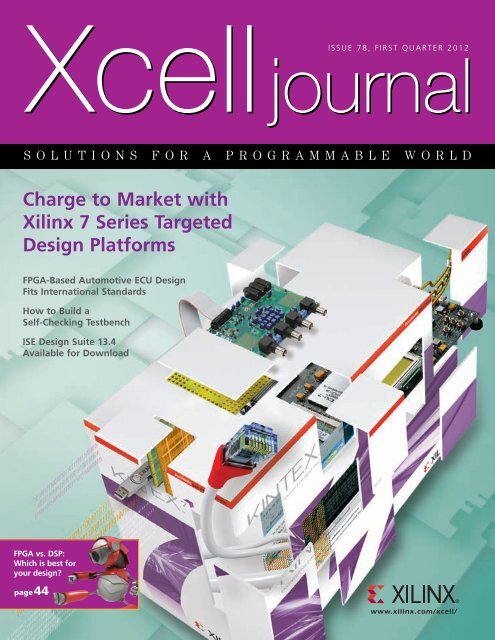
<strong>Charge</strong> <strong>to</strong> <strong>Market</strong> <strong>with</strong><br />
<strong>Xilinx</strong> 7 <strong>Series</strong> Targeted<br />
Design Platforms<br />
FPGA-Based Au<strong>to</strong>motive ECU Design<br />
Fits International Standards<br />
How <strong>to</strong> Build a<br />
Self-Checking Testbench<br />
ISE Design Suite 13.4<br />
Available for Download<br />
FPGA vs. DSP:<br />
Which is best for<br />
your design?<br />
page44<br />
www.xilinx.com/xcell/
Compact, Easy-<strong>to</strong>-Use Kit<br />
Demonstrates the Versatility<br />
of Spartan-6 FPGAs<br />
The low-cost Spartan ® -6 FPGA LX9 MicroBoard<br />
is the perfect solution for designers interested<br />
in exploring the MicroBlaze soft processor or<br />
Spartan-6 FPGAs in general. The kit comes <strong>with</strong><br />
several pre-built MicroBlaze “systems” allowing<br />
users <strong>to</strong> start software development just like<br />
any standard off-the-shelf microprocessor. The<br />
included Software Development Kit (SDK) provides<br />
a familiar Eclipse-based environment for writing and<br />
debugging code. Experienced FPGA users will find<br />
the MicroBoard a valuable <strong>to</strong>ol for general-purpose<br />
pro<strong>to</strong>typing and testing. The included peripherals<br />
and expansion interfaces make the kit ideal for a<br />
wide variety of applications.<br />
<strong>Xilinx</strong> ® Spartan ® -6 FPGA<br />
LX9 MicroBoard Features<br />
©Avnet, Inc. 2011. All rights reserved. AVNET is a registered trademark of Avnet, Inc.<br />
Avnet Spartan-6 FPGA LX9 MicroBoard<br />
ISE ® WebPACK ® software <strong>with</strong> device<br />
locked SDK and ChipScope licenses<br />
Micro-USB and USB extension cables<br />
Price: $89<br />
To purchase this kit, visit<br />
www.em.avnet.com/s6microboard<br />
or call 800.332.8638.
Add it up: 10 GbE, 40 GbE, and 100GbE ports offer more capacity and versatility than any High<br />
Speed Serial I/O board – ever. The <strong>Xilinx</strong>,Virtex 6, HXT FPGA provides user program-ability and data<br />
rates <strong>to</strong> 11 GB/s. ASIC designers, Network engineers, and IP developers, can use this <strong>to</strong>ol <strong>to</strong><br />
pro<strong>to</strong>type, emulate, model and test your most challenging projects. The board maybe used standalone,<br />
PCIe hosted, or plugged in<strong>to</strong> any Dini Group ASIC pro<strong>to</strong>typing board. Users will appreciate<br />
the scope of interfaces:<br />
• CFP Module—100 GbE or Single/Dual 40 GbE<br />
• 2-QSFP+ Modules—40 GbE<br />
• 4-SFP+ Modules—40 GbE<br />
• 8-SFP+ Modules—8 GbE<br />
All FPGA resources are user available and supported by a 240-pin DDR3<br />
UDIMM bulk memory. Daughter cards are accommodated for expansion,<br />
cus<strong>to</strong>mization, and FMC (Vita-57). Put your high speed serial designs <strong>to</strong> work.<br />
Here is a Dini board just for you.<br />
www.dinigroup.com • 7469 Draper Avenue • La Jolla, CA 92037 • (858) 454-3419 • e-mail: sales@dinigroup.com
<strong>Xcell</strong> journal<br />
PUBLISHER Mike Santarini<br />
mike.santarini@xilinx.com<br />
408-626-5981<br />
EDITOR Jacqueline Damian<br />
ART DIRECTOR Scott Blair<br />
DESIGN/PRODUCTION Teie, Gelwicks & Associates<br />
1-800-493-5551<br />
ADVERTISING SALES Dan Teie<br />
1-800-493-5551<br />
xcelladsales@aol.com<br />
INTERNATIONAL Melissa Zhang, Asia Pacific<br />
melissa.zhang@xilinx.com<br />
<strong>Xilinx</strong>, Inc.<br />
2100 Logic Drive<br />
San Jose, CA 95124-3400<br />
Phone: 408-559-77<strong>78</strong><br />
FAX: 408-879-4<strong>78</strong>0<br />
www.xilinx.com/xcell/<br />
Christelle Moraga, Europe/<br />
Middle East/Africa<br />
christelle.moraga@xilinx.com<br />
Miyuki Takegoshi, Japan<br />
miyuki.takegoshi@xilinx.com<br />
REPRINT ORDERS 1-800-493-5551<br />
www.xilinx.com/xcell/<br />
© 2012 <strong>Xilinx</strong>, Inc. All rights reserved. XILINX,<br />
the <strong>Xilinx</strong> Logo, and other designated brands included<br />
herein are trademarks of <strong>Xilinx</strong>, Inc. All other trademarks<br />
are the property of their respective owners.<br />
The articles, information, and other materials included<br />
in this issue are provided solely for the convenience of<br />
our readers. <strong>Xilinx</strong> makes no warranties, express,<br />
implied, statu<strong>to</strong>ry, or otherwise, and accepts no liability<br />
<strong>with</strong> respect <strong>to</strong> any such articles, information, or other<br />
materials or their use, and any use thereof is solely at<br />
the risk of the user. Any person or entity using such<br />
information in any way releases and waives any claim it<br />
might have against <strong>Xilinx</strong> for any loss, damage, or<br />
expense caused thereby.<br />
L E T T E R F R O M T H E P U B L I S H E R<br />
Peter Alfke Remembered, 1931-2011<br />
Not long ago we learned of the death of our old friend and <strong>Xilinx</strong> colleague Peter<br />
Alfke. If you’re a longtime <strong>Xilinx</strong> user or even new <strong>to</strong> FPGA design, chances are<br />
you’ve read some pearls of FPGA or general engineering wisdom from Peter at one<br />
time or another. He joined <strong>Xilinx</strong> in 1988 (employee number 109) as the direc<strong>to</strong>r of application<br />
engineering and later that year started <strong>Xcell</strong> <strong>Journal</strong>.<br />
Peter once <strong>to</strong>ld me that he came from a long line of educa<strong>to</strong>rs and had a passion for<br />
teaching. That’s why he loved being an FAE, started <strong>Xcell</strong> and later became the direc<strong>to</strong>r<br />
of technical applications at <strong>Xilinx</strong>, where he was responsible for technical cus<strong>to</strong>mer support,<br />
documentation and software QA. This passion for education and engineering was<br />
evident in his speeches and in his many writings—articles, forums and newsletters. In<br />
later years, he wrote the wonderfully practical “User<br />
Guide Lite” series that really cut <strong>to</strong> the good stuff,<br />
pointing users <strong>to</strong> the essentials of a given device. In<br />
the days when EE Times’ pldesignline.com would<br />
track “most read” and “most popular” articles, he <strong>to</strong>ok<br />
great pride in seeing each new <strong>to</strong>me sitting a<strong>to</strong>p both<br />
those lists—in some cases, for months.<br />
In September 2009 at the age of 77, he had been struggling<br />
<strong>with</strong> a growing list of health issues, and so one day<br />
at lunch, he turned <strong>to</strong> his group of friends sitting around<br />
the table and said, “Boys, I’ve decided <strong>to</strong> retire before<br />
they have <strong>to</strong> take me out of here on a stretcher.” We<br />
threw him a retirement party and I wrote a piece for EE<br />
Times announcing his departure. Peter was <strong>to</strong>uched by<br />
the response. He particularly loved one comment from a<br />
comp.arch.fpga member who wrote, “I use <strong>Xilinx</strong><br />
because Peter Alfke <strong>to</strong>ld me <strong>to</strong>.”<br />
Peter and I stayed in <strong>to</strong>uch after his retirement and whenever a new issue of <strong>Xcell</strong> <strong>Journal</strong><br />
came out, I would soon receive an e-mail or a call from Peter telling me what he liked or disliked<br />
about a particular article. At the same time, he would matter-of-factly mention that he<br />
was visiting a doc<strong>to</strong>r <strong>to</strong> have, first, a hip replacement, then a part of his lung removed and<br />
later, treatment for spreading cancer. One day I received a contributed piece on FIFOs that<br />
was a bit over my head. I naturally asked Peter <strong>to</strong> give it a read. He answered <strong>with</strong>in minutes.<br />
Michael, this is a bad paper.<br />
The author does not understand our asynchronous FIFO design, does not understand<br />
metastability issues and never explained the unorthodox features of his particular design.<br />
He writes 10 times faster in<strong>to</strong> than he reads from the FIFO. Nevertheless he worries<br />
about going empty ??? There must be some peculiar burst situations...<br />
Our FIFO is very sophisticated in resolving asynchronous timing issues, but is very<br />
straightforward in its functionality: Everything you write in<strong>to</strong> it, you must read out in<br />
the same sequence. Additional features, like idle codes, you should design as synchronous<br />
extensions on either side.<br />
I am back out of Stanford Hospital, recovering at home, but stuff like this will drive me<br />
out of bed anytime.<br />
Cheers,<br />
Peter<br />
Unfortunately, that was the last correspondence we had. And of course, I didn’t run the<br />
article. Who could argue <strong>with</strong> a legend?<br />
Mike Santarini<br />
Publisher<br />
Peter Alfke (second from right) on a 2008<br />
trip <strong>to</strong> CERN <strong>with</strong> <strong>Xilinx</strong> colleagues<br />
Patrick Lysaght (left) and Marc Defossez.
C O N T E N T S<br />
VIEWPOINTS XCELLENCE BY DESIGN<br />
20<br />
APPLICATION FEATURES<br />
Letter From the Publisher<br />
Peter Alfke<br />
Remembered, 1931-2011… 4<br />
Xpert Opinion<br />
Embedded Vision: FPGAs’<br />
Next Notable Technology<br />
Opportunity… 14<br />
32<br />
Cover S<strong>to</strong>ry<br />
<strong>Charge</strong> <strong>to</strong> <strong>Market</strong> <strong>with</strong><br />
<strong>Xilinx</strong> ®<br />
7 <strong>Series</strong> Targeted<br />
Design Platforms<br />
8<br />
<strong>Xcell</strong>ence in Au<strong>to</strong>motive<br />
FPGA-Based Au<strong>to</strong>motive ECU<br />
Design Addresses AUTOSAR,<br />
ISO 26262 Standards… 20<br />
<strong>Xcell</strong>ence in Pro<strong>to</strong>typing<br />
Lowering the Barriers<br />
<strong>to</strong> a Successful FPGA-Based<br />
Pro<strong>to</strong>type Project… 32
THE XILINX XPERIENCE FEATURES<br />
Xplanation: FPGA 101<br />
Ins and Outs of Digital Filter<br />
Design and Implementation… 36<br />
Xplanation: FPGA 101<br />
Using FPGAs <strong>to</strong> Solve Tough<br />
DSP Design Challenges… 42<br />
Xplanation: FPGA 101<br />
Tips and Tricks for Better Floating-Point<br />
Calculations in Embedded Systems… 48<br />
Ask FAE-X<br />
How <strong>to</strong> Build a<br />
Self-Checking Testbench… 52<br />
XTRA READING<br />
Tools of <strong>Xcell</strong>ence A new class of<br />
DC/DC turns down the noise… 58<br />
Xtra, Xtra The latest <strong>Xilinx</strong><br />
<strong>to</strong>ol updates and patches,<br />
as of January 2012… 64<br />
Xclamations! Share your wit and<br />
wisdom by supplying a caption for our<br />
techy car<strong>to</strong>on, for a chance <strong>to</strong> win an<br />
Avnet Spartan ® -6 LX9 MicroBoard… 66<br />
FIRST QUARTER 2012, ISSUE <strong>78</strong><br />
42<br />
Excellence in Magazine & <strong>Journal</strong> Writing<br />
2010, 2011<br />
2011<br />
36<br />
52<br />
Excellence in Magazine & <strong>Journal</strong> Design and Layout<br />
2010, 2011
COVER STORY<br />
<strong>Charge</strong> <strong>to</strong> <strong>Market</strong> <strong>with</strong><br />
<strong>Xilinx</strong> 7 <strong>Series</strong> Targeted<br />
Design Platforms<br />
Bored <strong>with</strong> just a board? New Kintex-7 and<br />
Virtex-7 kits accelerate FPGA development.<br />
by Mike Santarini<br />
Publisher, <strong>Xcell</strong> <strong>Journal</strong><br />
<strong>Xilinx</strong>, Inc.<br />
mike.santarini@xilinx.com<br />
8 <strong>Xcell</strong> <strong>Journal</strong> First Quarter 2012
To help cus<strong>to</strong>mers evaluate which<br />
FPGAs best suit their needs and get<br />
their designs up and running fast, <strong>Xilinx</strong><br />
Inc. has announced the release of the<br />
first three Targeted Design Platforms in<br />
support of its 28-nanometer, 7 series<br />
FPGAs. Base kits for the Virtex ® T<br />
-7 and<br />
Kintex-7 FPGAs include Agile Mixed-<br />
Signal daughtercards as well as industry-standard<br />
FMC connec<strong>to</strong>rs. In addition<br />
<strong>to</strong> these base kits, Avnet is also<br />
releasing its <strong>Xilinx</strong> Kintex-7 FPGA DSP<br />
Kit for cus<strong>to</strong>mers eager <strong>to</strong> take advantage<br />
of the fact that FPGAs can do the<br />
job of multiple DSPs and perform faster.<br />
The three new kits represent the<br />
first deliverables of <strong>Xilinx</strong>’s secondgeneration<br />
platforms for FPGA system<br />
development. <strong>Xilinx</strong> introduced<br />
its Targeted Design Platform (TDP)<br />
strategy back in 2009 in support of its<br />
6 series devices (see cover s<strong>to</strong>ry, <strong>Xcell</strong><br />
<strong>Journal</strong> <strong>Issue</strong> 68). <strong>Xilinx</strong> describes<br />
the platform strategy as a pyramid<br />
consisting of four layers: base platforms,<br />
domain-specific platforms,<br />
market-specific platforms and, at the<br />
apex, cus<strong>to</strong>mer designs (Figure 1).<br />
The TDP approach allows cus<strong>to</strong>mers<br />
<strong>to</strong> take advantage of prebuilt solutions<br />
from <strong>Xilinx</strong> and the <strong>Xilinx</strong><br />
ecosystem, and easily add these <strong>to</strong><br />
their FPGA design projects. With the<br />
TDP as their design’s foundation, cus<strong>to</strong>mers<br />
can focus on features that will<br />
differentiate their products.<br />
COVER STORY<br />
In the <strong>Xilinx</strong> TDP hierarchy, base<br />
platforms like the new Virtex-7 FPGA<br />
VC707 Evaluation Kit and Kintex-7<br />
FPGA KC705 Evaluation Kit are the primary<br />
means for evaluating <strong>Xilinx</strong>’s<br />
device families. On <strong>to</strong>p of the base<br />
TDPs, domain-specific kits like the one<br />
from Avnet further help cus<strong>to</strong>mers targeting<br />
designs in the DSP, embedded<br />
and connectivity domains. For even<br />
greater design acceleration, <strong>Xilinx</strong> also<br />
offers market-specific development<br />
platforms for segments such as aerospace<br />
and defense, au<strong>to</strong>motive, consumer,<br />
wireless and wired communications,<br />
professional broadcast and industrial,<br />
scientific and medical. Versions of<br />
these market-specific kits for the 7<br />
series are forthcoming.<br />
All <strong>Xilinx</strong> TDPs include not only<br />
development boards and the software<br />
<strong>to</strong> program the FPGAs, but also internal<br />
and third-party IP, reference designs<br />
and documentation, and a broad portfolio<br />
of internally and partner-developed<br />
FPGA Mezzanine Card (FMC) daughtercards.<br />
All these assets combine in<strong>to</strong><br />
a powerful vehicle <strong>to</strong> help users get<br />
their designs working at a system level<br />
sooner than ever before possible.<br />
<strong>Xilinx</strong> offers all three types of<br />
TDPs for its 6 series devices and is<br />
now beginning <strong>to</strong> roll out the TDPs<br />
for the 7 series. The VC707, KC705<br />
and Kintex DSP Kit are the first of<br />
many 7 series kits that will debut in<br />
the coming months.<br />
Mark Moran, senior strategic marketing<br />
manager <strong>with</strong> <strong>Xilinx</strong>, is emphatic<br />
in noting that TDPs are not your traditional<br />
development kits. All programmable<br />
chip vendors offer kits,<br />
which usually include a development<br />
board, a power cord, software and<br />
sometimes connec<strong>to</strong>rs.<br />
“In a typical kit, you load the software<br />
in<strong>to</strong> your PC, plug in the board,<br />
power it up and pretty much all you<br />
see is an LED light up <strong>to</strong> let you know<br />
it’s working…and that’s it,” said<br />
Moran. “If you want more, you typically<br />
First Quarter 2012 <strong>Xcell</strong> <strong>Journal</strong> 9
COVER STORY<br />
CUSTOMER INNOVATION<br />
have <strong>to</strong> go <strong>to</strong> the vendor’s website <strong>to</strong><br />
search for documentation and IP that’s<br />
appropriate for your chip and board.<br />
In most cases, you’ll be lucky if you<br />
find even basic building blocks. And if<br />
you do, they are often out of date.<br />
Some vendors may even require that<br />
you purchase standard IP blocks just<br />
<strong>to</strong> get up and running. Buying a kit at<br />
some vendors is a lot like buying a car<br />
<strong>with</strong>out tires—you can sit in the driver’s<br />
seat and turn it on, but you can’t<br />
drive it anywhere.”<br />
Worse, many chip vendors offer a<br />
dizzying array of kits <strong>with</strong> overlapping<br />
purposes. That, he said, makes it hard<br />
for the user <strong>to</strong> discern which one is<br />
best, while at the same time making it<br />
difficult for the vendor <strong>to</strong> offer quality<br />
support. “With the Targeted Design<br />
Platform approach, <strong>Xilinx</strong> is offering a<br />
lot more than what folks find in a typical<br />
kit,” said Moran. “Instead of a car <strong>with</strong><br />
no tires, we are offering the board equivalent<br />
<strong>to</strong> a Ferrari that has race tires<br />
installed, a full tank of gas, is tuned up<br />
and ready <strong>to</strong> go—ready <strong>to</strong> go fast.”<br />
Evan Leal, senior product marketing<br />
manager, Targeted Design Platforms, at<br />
<strong>Xilinx</strong>, said that in addition <strong>to</strong> the<br />
board, connec<strong>to</strong>rs and design software,<br />
Targeted Design Platform kits include<br />
multiple types of reference designs,<br />
free IP and, in some cases, bundled<br />
FMC cards. There is immediate access<br />
<strong>to</strong> IP libraries and a catalog of plug-and-<br />
FOCUS ON DIFFERENTIATION<br />
WIRED, WIRELESS, BROADCAST, DEFENSE, CONSUMER AND MORE<br />
EMBEDDED, DSP, CONNECTIVITY, ANALOG, VIDEO<br />
DOMAIN IP, DOMAIN TOOLS, FMC RADIO DAUGHTERCARDS<br />
ARTIX KINTEX VIRTEX<br />
BASE IP, ISE DESIGN SUITE, BASE BOARDS<br />
Figure 1 – The <strong>Xilinx</strong> Targeted Design Platform concept allows users <strong>to</strong> focus their design efforts<br />
on product differentiation and get products <strong>to</strong> market quickly.<br />
play FMC daughtercards from <strong>Xilinx</strong><br />
and third-party vendors. “Because this<br />
is our second TDP generation, we<br />
already have in place a very formidable<br />
ecosystem <strong>to</strong> support these new kits,”<br />
said Moran. “Further, <strong>with</strong> this generation<br />
of devices we’ve made it even easier<br />
for cus<strong>to</strong>mers <strong>to</strong> get up and running<br />
quickly.” The hundreds of board, design<br />
service, IP and <strong>to</strong>ol vendors that make<br />
up the <strong>Xilinx</strong> Alliance Program<br />
(http://www.xilinx.com/alliance/index<br />
.htm) provide a rich diversity of solutions<br />
and applications that enable<br />
<strong>Xilinx</strong> Targeted Design Platforms.<br />
<strong>Xilinx</strong> worked closely <strong>with</strong> 4DSP Inc.,<br />
Analog Devices Inc., Avnet, Northwest<br />
Logic, The Mathworks, Texas<br />
Instruments and Xylon <strong>to</strong> bring the<br />
Kintex-7 FPGA and Virtex-7 FPGA<br />
kits <strong>to</strong> market.<br />
PLUG-AND-PLAY FMC CARDS<br />
In fact, one of the keys <strong>to</strong> <strong>Xilinx</strong>’s TDP<br />
approach is the industry-standard FMC<br />
connec<strong>to</strong>rs on all kits starting <strong>with</strong><br />
those supporting Virtex-6 and Spartan ® -<br />
6 FPGA families. The addition of FMC<br />
connec<strong>to</strong>rs allows IP vendors, fellow<br />
chip makers and design services companies<br />
<strong>to</strong> field daughtercards that<br />
designers can use <strong>to</strong> quickly connect<br />
boards <strong>to</strong> <strong>Xilinx</strong> kits and test their<br />
designs <strong>with</strong>in a system-level context.<br />
Moran said that since its launch<br />
<strong>with</strong> the 6 series in 2009, the TDP<br />
CUSTOMER DESIGN<br />
MARKET-SPECIFIC<br />
DOMAIN-SPECIFIC<br />
BASE PLATFORM<br />
ecosystem now boasts more than 100<br />
FMC cards from over 30 partners. In<br />
recent months, <strong>Xilinx</strong> has held<br />
plugfests in which more than 30 of<br />
these FMCs have been verified <strong>to</strong><br />
work <strong>with</strong> the new 7 series platforms,<br />
covering a wide range of applications.<br />
In the coming months <strong>Xilinx</strong> anticipates<br />
a greater number of FMC cards<br />
will become available.<br />
The 7 series also lends some inherent<br />
improvements <strong>to</strong> the TDP strategy.<br />
For example, Moran points out that<br />
<strong>with</strong> the introduction of the 7 series<br />
devices last year, <strong>Xilinx</strong> embraced the<br />
ARM ® AMBA ® AXI4 interface. AXI4<br />
allows users <strong>to</strong> more easily integrate<br />
<strong>Xilinx</strong>, third-party and internally<br />
developed IP in<strong>to</strong> <strong>Xilinx</strong> 7 series<br />
devices. It also allows cus<strong>to</strong>mers and<br />
the <strong>Xilinx</strong> IP ecosystem <strong>to</strong> focus on<br />
one IP interconnect structure rather<br />
than several, so as <strong>to</strong> refine IP offerings<br />
and develop new ones faster.<br />
Another key benefit of the new-generation<br />
TDPs comes from the fact that<br />
<strong>Xilinx</strong> implemented all its 7 series<br />
devices—the Virtex-7, Kintex-7 and<br />
Artix-7—as well as the Zynq-7000<br />
Extensible Processing Platform<br />
devices on a scalable programmable<br />
logic architecture. Moran said this unified<br />
architecture allows users <strong>to</strong> implement<br />
their IP and migrate their designs<br />
more easily between FPGA families as<br />
their design requirements evolve. This<br />
10 <strong>Xcell</strong> <strong>Journal</strong> First Quarter 2012
simplifies and streamlines design reuse<br />
and evaluation for end users.<br />
Moran said that another huge bonus<br />
of the 7 series is that even the Kintex-7<br />
devices now include Agile Mixed-Signal<br />
(AMS) blocks, which allow users <strong>to</strong><br />
moni<strong>to</strong>r and test the internal blocks in<br />
the design and even implement analog<br />
functions (such as ADCs) on the FPGA<br />
itself, instead of on discrete external circuitry.<br />
Doing so improves performance,<br />
saves board space and reduces the bill<br />
of materials. It also allows users <strong>to</strong> moni<strong>to</strong>r<br />
the power consumption of the<br />
device and confirms the superiority of<br />
the <strong>Xilinx</strong> 7 series over competing<br />
devices, he said (see cover s<strong>to</strong>ry, <strong>Xcell</strong><br />
<strong>Journal</strong> <strong>Issue</strong> 76).<br />
“This AMS block has been a feature<br />
that up until the 7 series we’ve only had<br />
in our Virtex devices,” said Moran.<br />
“With the 7 series, the AMS block is<br />
available in our Kintex devices as well.<br />
There will be a whole new group of<br />
users that will now be able <strong>to</strong> reap<br />
great benefits from these blocks.”<br />
Moran said the first three 7 series<br />
TDPs are loaded <strong>with</strong> features <strong>to</strong> help<br />
users get up and designing extremely<br />
fast. The feature set of each of these<br />
kits is quite extensive and can be<br />
found on www.xilinx.com. Moran and<br />
Leal walked us through the high points<br />
of each.<br />
THE VIRTEX-7 FPGA VC707<br />
EVALUATION KIT<br />
The <strong>Xilinx</strong> Virtex-7 FPGA VC707 Evaluation<br />
Kit is the base TDP for designers<br />
looking for a combination of break-<br />
through performance, capacity and<br />
power efficiency required in the many<br />
applications the Virtex-7 FPGA serves,<br />
Moran said. These include advanced systems<br />
for wired and wireless communications,<br />
aerospace and defense, medical<br />
and broadcasting markets (Figure 2).<br />
This kit is based specifically on the<br />
VX485T-2 FPGA, a midsize Virtex-7<br />
FPGA device.<br />
In terms of software, it comes <strong>with</strong><br />
an ISE ® Design Suite Logic edition<br />
that is device-locked <strong>to</strong> the Virtex-7<br />
VX485T-2 FPGA. For serial connectivity,<br />
it has Gigabit Ethernet (GMII,<br />
COVER STORY<br />
Even the Kintex devices now include Agile Mixed-Signal technology.<br />
AMS blocks allow users <strong>to</strong> moni<strong>to</strong>r and test the internal blocks in<br />
the design and even implement analog functions on the FPGA<br />
itself instead of on discrete external circuitry. This improves<br />
performance, saves board space and reduces the bill of materials.<br />
RGMII and SGMII), an SFP/SFP+ transceiver<br />
connec<strong>to</strong>r, a GTX port (TX, RX)<br />
<strong>with</strong> four SMA connec<strong>to</strong>rs and a PCI<br />
Express ® x8 edge connec<strong>to</strong>r.<br />
For parallel connectivity, the kit has<br />
two FMC-HPC connec<strong>to</strong>rs (eight GTX<br />
Figure 2 – The <strong>Xilinx</strong> Virtex-7 FPGA VC707 Evaluation Kit is the base TDP for designers<br />
looking for a combination of breakthrough performance, capacity and power efficiency<br />
required in the many applications the Virtex-7 FPGA serves.<br />
transceivers, 160 single-ended or 80 differential<br />
user-defined signals). For<br />
memory, it includes SODIMM DDR3<br />
memory at 1,600 Mbps, a 1-Gbit (128-<br />
Mbyte) BPI flash for PCIe ® configuration,<br />
an SD card interface and an 8kbyte<br />
IIC EEPROM.<br />
Additional connectivity includes<br />
HDMI video out, a UART-<strong>to</strong>-USB<br />
First Quarter 2012 <strong>Xcell</strong> <strong>Journal</strong> 11
COVER STORY<br />
The ROHS-compliant Kintex-7 FPGA KC705 Evaluation Kit<br />
includes a number of high-impact and cost-saving features. It's built<br />
for maximum flexibility, <strong>to</strong> accelerate a broad range of applications.<br />
bridge, a 2x16 LCD header, 8x LEDs,<br />
IIC and an analog mixed-signal port.<br />
“This evaluation kit comes <strong>with</strong> an<br />
AMS evaluation card <strong>to</strong> help designers<br />
quickly assess the value of the AMS<br />
feature,” said Leal.<br />
The kit also comes <strong>with</strong> reference<br />
designs and demonstrations, along<br />
<strong>with</strong> comprehensive documentation <strong>to</strong><br />
allow users <strong>to</strong> get <strong>to</strong> work immediately.<br />
Example designs and demonstrations<br />
include a board diagnostic demo,<br />
ChipScope Pro Serial I/O Toolkit,<br />
IBERT transceiver test design, multiboot<br />
reference design, PCI Express<br />
Gen 2 (x8) test design and DDR3 memory<br />
interface design.<br />
In terms of documentation, the kit<br />
includes a Getting Started Guide,<br />
Hardware User’s Guide and Reference<br />
Design and Example Guide. It also<br />
comes <strong>with</strong> schematics and UCF files,<br />
providing the information needed <strong>to</strong><br />
accelerate board layout and development<br />
based upon best practices.<br />
For further details about the board<br />
such as device configuration, clocking,<br />
controls and power, visit the Virtex-7<br />
FPGA VC707 Evaluation Kit TDP kit<br />
page at http://www.xilinx.com/<br />
products/boards-and-kits/EK-V7-<br />
VC707-G.htm.<br />
KINTEX-7 FPGA KC705<br />
EVALUATION KIT<br />
The base TDP for the Kintex-7 family is<br />
the Kintex-7 FPGA KC705 Evaluation<br />
Kit, featuring an XC7K325T-FF900-2<br />
FPGA. Moran said the kit is built for<br />
maximum flexibility <strong>to</strong> help designers<br />
accelerate development of a broad<br />
range of applications, including<br />
radio/baseband, radar, Edge QAM,<br />
triple-rate SDI and others that demand<br />
power-efficient, high-speed communications<br />
and processing (Figure 3).<br />
The ROHS-compliant Kintex-7 FPGA<br />
KC705 Evaluation Kit includes a number<br />
of high-impact and cost-saving features.<br />
It comes <strong>with</strong> the ISE Design<br />
Suite: Logic Edition device-locked <strong>to</strong><br />
the Kintex-7 XC7K325T FPGA.<br />
Serial connectivity includes Gigabit<br />
Ethernet, SFP/SFP+ transceiver connec<strong>to</strong>r,<br />
a GTX port (TX, RX) <strong>with</strong> four SMA<br />
connec<strong>to</strong>rs, a UART-<strong>to</strong>-USB bridge and<br />
a PCI Express x8 edge connec<strong>to</strong>r.<br />
Parallel connectivity includes an<br />
FMC-HPC connec<strong>to</strong>r (four GTX transceivers,<br />
116 single-ended or 58 differential—34<br />
LA and 24 HA—user-defined signals)<br />
and an FMC-LPC connec<strong>to</strong>r (one<br />
GTX transceiver, 68 single-ended or 34<br />
differential user-defined signals).<br />
Additional connectivity includes<br />
HDMI video out, a 2x16 LCD display<br />
connec<strong>to</strong>r, 8x LEDs, IIC, LCD header<br />
and an analog mixed-signal port.<br />
Memory includes SODIMM DDR3<br />
memory at 1,600 Mbps, a 1-Gbit (128-<br />
Mbyte) BPI flash for PCIe configuration,<br />
an SDIO-SD card interface, a 16-<br />
Mbyte quad SPI flash and an 8-kbyte<br />
IIC EEPROM.<br />
The kit includes a board diagnostic<br />
demo, a ChipScope Pro Serial I/O<br />
Toolkit, an IBERT transceiver test<br />
Figure 3 – The Kintex-7 FPGA KC705 Evaluation Kit is aimed at a broad range of applications<br />
that demand power-efficient, high-speed communications and processing.<br />
design, a multiboot reference design, a<br />
PCI Express Gen 2 (x8) test design and<br />
a DDR3 memory interface design.<br />
“Further, this evaluation kit comes <strong>with</strong><br />
a targeted reference design featuring<br />
PCIe x4 Gen 2 and DDR3 <strong>to</strong> enable<br />
designers <strong>to</strong> get started quickly integrating<br />
some of the most popular features<br />
used by FPGA designers,” said Leal.<br />
Documentation includes a Getting<br />
Started Guide, Hardware User’s Guide,<br />
12 <strong>Xcell</strong> <strong>Journal</strong> First Quarter 2012
Figure 4 – The Kintex-7 FPGA DSP Kit from Avnet targets cus<strong>to</strong>mers looking <strong>to</strong><br />
use FPGAs <strong>to</strong> do the job of multiple DSPs, and do it faster.<br />
Reference Design and Example User<br />
Guide, along <strong>with</strong> schematics and<br />
UCF files. “Like the VC707, the KC705<br />
Evaluation Kit comes <strong>with</strong> an AMS<br />
evaluation card <strong>to</strong> help designers<br />
quickly assess the value of the AMS<br />
feature,” said Leal.<br />
It also comes <strong>with</strong> a number of<br />
cables and adapters (namely, a universal<br />
12-volt power supply, two USB<br />
cables, one Ethernet cable and one<br />
HDMI-<strong>to</strong>-DVI adapter).<br />
For further details about the board<br />
such as device configuration, clocking,<br />
controls and power, visit the<br />
Kintex-7 FPGA KC705 Evaluation Kit<br />
TDP kit page at http://www.xilinx.com/<br />
products/boards-and-kits/EK-K7-<br />
KC705-G.htm.<br />
THE KINTEX-7 FPGA DSP KIT<br />
In addition <strong>to</strong> these base platforms,<br />
Avnet is releasing the <strong>Xilinx</strong> Kintex-7<br />
FPGA DSP Kit Targeted Design Platform<br />
for cus<strong>to</strong>mers looking <strong>to</strong> use<br />
FPGAs <strong>to</strong> do the job of multiple<br />
DSPs—and do it faster. Built around<br />
the Kintex-7 KX325T FPGA, the TDP<br />
includes an integrated high-speed<br />
analog FMC <strong>to</strong> interface <strong>to</strong> realworld<br />
signals (Figure 4).<br />
The high-speed analog daughtercard<br />
is the FMC150 by 4DSP. This<br />
card provides two 14-bit, 250-<br />
Msample/second A/D channels and<br />
two 16-bit, 800-MSPS D/A channels<br />
that can be clocked by an internal<br />
clock source or an externally supplied<br />
sample clock.<br />
The Kintex-7 DSP kit ships <strong>with</strong> a<br />
targeted DSP reference design that<br />
includes a high-speed analog interface<br />
<strong>with</strong> digital upconversion (DUC)<br />
and digital downconversion (DDC).<br />
End users can place it right in<strong>to</strong> their<br />
designs, saving weeks of development<br />
time.<br />
For further details about the board<br />
such as device configuration, clocking,<br />
controls and power, visit the<br />
Kintex-7 FPGA DSP Kit page at<br />
http://www.xilinx.com/products/boards<br />
-and-kits/AES-K7DSP-325T-G.htm.<br />
In the coming months, <strong>Xilinx</strong> will be<br />
releasing several new boards in support<br />
of its 7 series devices. To see what<br />
boards are available <strong>to</strong>day and <strong>to</strong> learn<br />
more, visit http://www.xilinx.com/<br />
products/boards-and-kits/index.htm.<br />
To learn more about FMC daughtercards,<br />
visit http://www.xilinx.com/<br />
products/boards_kits/fmc.htm.<br />
COVER STORY<br />
First Quarter 2012 <strong>Xcell</strong> <strong>Journal</strong> 13
XPERT OPINION<br />
Embedded Vision:<br />
FPGAs’ Next Notable<br />
Technology Opportunity<br />
By Brian Dipert<br />
Edi<strong>to</strong>r-In-Chief<br />
Embedded Vision Alliance<br />
dipert@embedded-vision.com<br />
José Alvarez<br />
Engineering Direc<strong>to</strong>r, Video Technology<br />
<strong>Xilinx</strong>, Inc.<br />
jose.alvarez@xilinx.com<br />
Mihran Touriguian<br />
Senior DSP Engineer<br />
BDTI (Berkeley Design Technology, Inc.)<br />
<strong>to</strong>uriguian@bdti.com<br />
14 <strong>Xcell</strong> <strong>Journal</strong> First Quarter 2012
A jointly developed reference<br />
design validates the potential<br />
of <strong>Xilinx</strong>’s Zynq device in a<br />
burgeoning application category.<br />
What up-and-coming innovation<br />
can help you design a<br />
system that alerts users <strong>to</strong><br />
a child struggling in a swimming pool,<br />
or <strong>to</strong> an intruder attempting <strong>to</strong> enter a<br />
residence or business? It’s the same<br />
technology that can warn drivers of<br />
impending hazards on the roadway,<br />
and even prevent them from executing<br />
lane-change, acceleration and<br />
other maneuvers that would be hazardous<br />
<strong>to</strong> themselves and others. It<br />
can equip a military drone or other<br />
robot <strong>with</strong> electronic “eyes” that<br />
enable limited-<strong>to</strong>-full au<strong>to</strong>nomous<br />
operation. It can assist a human<br />
physician in diagnosing a patient’s illness.<br />
It can uniquely identify a face,<br />
subsequently initiating a variety of<br />
actions (au<strong>to</strong>matically logging in<strong>to</strong> a<br />
user account, for example, or pulling<br />
up relevant news and other information),<br />
interpreting gestures and even<br />
discerning a person’s emotional state.<br />
And in conjunction <strong>with</strong> GPS, compass,<br />
accelerometer, gyroscope and<br />
other features, it can deliver a dataaugmented<br />
presentation of a scene.<br />
The technology common <strong>to</strong> all of<br />
these application examples is embedded<br />
vision, which is poised <strong>to</strong> enable<br />
the next generation of electronic-system<br />
success s<strong>to</strong>ries. Embedded vision<br />
got its start in traditional computer<br />
vision applications such as assembly<br />
line inspection, optical character<br />
recognition, robotics, surveillance and<br />
military systems. In recent years, however,<br />
the decreasing costs and increasing<br />
capabilities of key technology<br />
building blocks have broadened and<br />
accelerated vision’s penetration in<strong>to</strong><br />
key high-volume markets.<br />
Driven by expanding and evolving<br />
application demands, for example,<br />
image sensors are making notable<br />
improvements in key attributes such<br />
as resolution, low-light performance,<br />
frame rate, size, power consumption<br />
and cost. Similarly, embedded vision<br />
applications require processors <strong>with</strong><br />
high performance, low prices, low<br />
power consumption and flexible programmability,<br />
all ideal attributes that<br />
are increasingly becoming a reality in<br />
numerous product implementation<br />
forms. Similar benefits are being<br />
accrued by latest-generation optics<br />
systems, lighting modules, volatile and<br />
nonvolatile memories, and I/O standards.<br />
And algorithms are up <strong>to</strong> the<br />
challenge, leveraging these hardware<br />
improvements <strong>to</strong> deliver more robust<br />
and reliable analysis results.<br />
Embedded vision refers <strong>to</strong> machines<br />
that understand their environment<br />
through visual means. By “embedded,”<br />
we’re referring <strong>to</strong> any image-sensorinclusive<br />
system that isn’t a general-purpose<br />
computer. Embedded might mean,<br />
for example, a cellular phone or tablet<br />
computer, a surveillance system, an<br />
earth-bound or flight-capable robot, a<br />
vehicle containing a 360° suite of cameras<br />
or a medical diagnostic device. Or<br />
it could be a wired or wireless user<br />
interface peripheral; Microsoft’s Kinect<br />
for the Xbox 360 game console, perhaps<br />
the best-known example of this latter<br />
category, sold 8 million units in its first<br />
two months on the market.<br />
THE FPGA OPPORTUNITY:<br />
A CASE STUDY<br />
A diversity of robust embedded vision<br />
processing product options exist:<br />
XPERT OPINION<br />
microprocessors and embedded controllers,<br />
application-tailored SoCs,<br />
DSPs, graphics processors, ASICs<br />
and FPGAs. An FPGA is an intriguing<br />
silicon platform for realizing embedded<br />
vision, because it approximates<br />
the combination of the hardware<br />
attributes of an ASIC—high performance<br />
and low power consumption—<br />
<strong>with</strong> the flexibility and time-<strong>to</strong>-market<br />
advantages of the software algorithm<br />
alternative running on a CPU,<br />
GPU or DSP. Flexibility is a particularly<br />
important fac<strong>to</strong>r at this nascent<br />
stage in embedded vision’s market<br />
development, where both rapid bug<br />
fixes and feature set improvements<br />
are the norm rather than the exception,<br />
as is the desire <strong>to</strong> support a<br />
diversity of algorithm options. An<br />
FPGA’s hardware configurability also<br />
enables straightforward design adaptation<br />
<strong>to</strong> image sensors supporting<br />
various serial and parallel (and analog<br />
and digital) interfaces.<br />
The Embedded Vision Alliance is a<br />
unified worldwide alliance of technology<br />
developers and providers chartered<br />
<strong>with</strong> transforming embedded vision’s<br />
potential in<strong>to</strong> reality in a rich, rapid<br />
and efficient manner (see sidebar).<br />
Two of its founding members, BDTI<br />
(Berkeley Design Technology, Inc.) and<br />
<strong>Xilinx</strong>, partnered <strong>to</strong> co-develop a reference<br />
design that exemplifies not only<br />
embedded vision’s compelling promise<br />
but also the role that FPGAs might play<br />
in actualizing it. The goal of the project<br />
was <strong>to</strong> explore the typical architectural<br />
decisions a system designer would<br />
make when creating highly complex<br />
intelligent vision platforms containing<br />
elements requiring intensive hardware<br />
processing and complex software and<br />
algorithmic control.<br />
BDTI and <strong>Xilinx</strong> partitioned the<br />
design so that the FPGA fabric would<br />
handle digital signal-processing-intensive<br />
operations, <strong>with</strong> a CPU performing<br />
complex control and prediction<br />
algorithms. The explora<strong>to</strong>ry implementation<br />
described here connected the<br />
CPU board <strong>to</strong> the FPGA board via an<br />
First Quarter 2012 <strong>Xcell</strong> <strong>Journal</strong> 15
XPERT OPINION<br />
Ethernet interface. The FPGA performed<br />
high-bandwidth processing,<br />
<strong>with</strong> only metadata interchanged<br />
through the network tether. This project<br />
also explored the simultaneous development<br />
of hardware and software,<br />
which required the use of accurate simulation<br />
models well ahead of the final<br />
FPGA hardware implementation.<br />
PHASE 1: ROAD SIGN DETECTION<br />
This portion of the project, along <strong>with</strong><br />
the next phase, leveraged two specific<br />
PC-based functions: a simulation<br />
model of under-development <strong>Xilinx</strong><br />
video IP blocks, and a BDTI-developed<br />
processing application (Figure<br />
1). The input data consisted of a 720p<br />
HD resolution, 60-frame/second (fps)<br />
YUV-encoded video stream representing<br />
the images that a vehicle’s frontfacing<br />
camera might capture. And the<br />
goal was <strong>to</strong> identify (albeit not “read”<br />
using optical character recognition,<br />
although such an added capability<br />
would be a natural extension) four<br />
types of objects in the video frames<br />
as a driver-assistance scheme:<br />
• Green directional signs<br />
• Yellow and orange hazard signs<br />
• Blue informational signs, and<br />
• Orange traffic barrels<br />
The <strong>Xilinx</strong>-provided IP block simulation<br />
models output metadata that<br />
identified the locations and sizes of<br />
various-colored groups of pixels in<br />
each frame, the very same metadata<br />
generated by the final hardware IP<br />
blocks. The accuracy of many embedded<br />
vision systems is affected by<br />
external fac<strong>to</strong>rs such as noise from<br />
imaging sensors, unexpected changes<br />
in illumination and unpredictable<br />
external motion. The mandate for this<br />
project was <strong>to</strong> allow the FPGA hardware<br />
<strong>to</strong> process the images and create<br />
metadata in the presence of external<br />
disturbances <strong>with</strong> parsimonious<br />
use of hardware resources, augmented<br />
by predictive software that would<br />
allow for such disturbances <strong>with</strong>out<br />
decreasing detection accuracy.<br />
BDTI optimized the IP blocks’<br />
extensive set of configuration parameters<br />
for the particular application in<br />
question, and BDTI’s postprocessing<br />
algorithms provided further refinement<br />
and prediction capabilities. In some<br />
cases, for example, the hardware was<br />
only partially able <strong>to</strong> identify the<br />
objects in one frame, but the application-layer<br />
software continued <strong>to</strong> predict<br />
the location of the object using<br />
tracking algorithms. This approach<br />
worked very well, since in many cases<br />
the physical detection may not be consistent<br />
across time. Therefore, the software<br />
intelligent layer is the key <strong>to</strong> providing<br />
consistent prediction.<br />
As another example, black or white<br />
letters contained <strong>with</strong>in a green highway<br />
sign might confuse the IP blocks’<br />
generic image-analysis functions, there-<br />
EMBEDDED VISION ALLIANCE SEES SUCCESS<br />
Embedded vision technology has the potential <strong>to</strong><br />
enable a wide range of electronic products that<br />
are more intelligent and responsive than before,<br />
and thus more valuable <strong>to</strong> users. It can add helpful features<br />
<strong>to</strong> existing products. And it can provide significant<br />
new markets for hardware, software and semiconduc<strong>to</strong>r<br />
manufacturers. The Embedded Vision Alliance,<br />
a unified worldwide organization of technology developers<br />
and providers, will transform this potential in<strong>to</strong><br />
reality in a rich, rapid and efficient manner.<br />
The alliance has developed a full-featured website,<br />
freely accessible <strong>to</strong> all and including (among other things)<br />
articles, videos, a daily news portal and a multisubject discussion<br />
forum staffed by a diversity of technology experts.<br />
Registered website users can receive the alliance’s monthly<br />
e-mail newsletter; they also gain access <strong>to</strong> the Embedded<br />
Vision Academy, containing numerous tu<strong>to</strong>rial presentations,<br />
technical papers and file downloads, intended <strong>to</strong><br />
enable new players in the embedded vision application<br />
space <strong>to</strong> rapidly ramp up their expertise.<br />
Other envisioned future aspects of the alliance’s charter<br />
may include:<br />
■ The incorporation, and commercialization, of technology<br />
breakthroughs originating in universities and research<br />
labora<strong>to</strong>ries around the world,<br />
■ The codification of hardware, semiconduc<strong>to</strong>r and software<br />
standards that will accelerate new technology<br />
adoption by eliminating the confusion and inefficiency<br />
of numerous redundant implementation alternatives,<br />
■ Development of robust benchmarks <strong>to</strong> enable clear and<br />
comprehensive evaluation and selection of various<br />
embedded vision system building blocks, such as<br />
processors and software algorithms, and<br />
■ The proliferation of hardware and software reference<br />
designs, emula<strong>to</strong>rs and other development aids that will<br />
enable component suppliers, systems implementers<br />
and end cus<strong>to</strong>mers <strong>to</strong> develop and select products that<br />
optimally meet unique application needs.<br />
For more information, please visit www.embedded-vision.com. Contact the Embedded Vision Alliance at<br />
info@embedded-vision.com and (510) 451-1800. – Brian Dipert<br />
16 <strong>Xcell</strong> <strong>Journal</strong> First Quarter 2012
Model<br />
Config.<br />
File<br />
MATLAB Model of the <strong>Xilinx</strong> Video Analytics IP<br />
Metadata<br />
File<br />
Appl.<br />
Config.<br />
File<br />
Road sign recognition using<br />
<strong>Xilinx</strong> IP only<br />
Road signs are split<br />
by incorrectly subdividing the sign in<strong>to</strong><br />
multiple-pixel subgroups (Figure 2).<br />
The IP blocks might also incorrectly<br />
interpret other vehicles’ rear driving or<br />
brake lights as cones or signs by confusing<br />
red <strong>with</strong> orange, depending on<br />
the quality and setup of the imaging<br />
sensor used for the application.<br />
The BDTI-developed algorithms<br />
therefore served <strong>to</strong> further process the<br />
<strong>Xilinx</strong>-supplied metadata in an appli-<br />
Parser Tracker Identifier<br />
Get one<br />
frame of<br />
metadata,<br />
parse and<br />
preclassify<br />
Match metadata<br />
objects <strong>to</strong><br />
tracked objects<br />
Host PC<br />
Predict motion<br />
of each<br />
tracked object<br />
Tracked<br />
objects list<br />
Once per frame<br />
Identify tracked<br />
objects by<br />
category<br />
cation-tailored manner. They knew, for<br />
example, what signs were supposed <strong>to</strong><br />
look like (size, shape, color, pattern,<br />
location <strong>with</strong>in the frame and so on),<br />
and therefore were able <strong>to</strong> combine<br />
relevant pixel clusters in<strong>to</strong> larger<br />
groups. Similarly, the algorithms determined<br />
when it was appropriate <strong>to</strong> discard<br />
seemingly close-in-color pixel<br />
clusters that weren’t signs, such as the<br />
aforementioned vehicle brake lights.<br />
XPERT OPINION<br />
PHASE 2: PEDESTRIAN<br />
DETECTION AND TRACKING<br />
In the first phase of this project, the<br />
camera was in motion but the objects<br />
(that is, signs) being recognized were<br />
stationary. In the second phase targeting<br />
security, on the other hand, the<br />
camera was stationary but objects<br />
(people, in this case) were not. Also,<br />
this time the video-analytics algorithms<br />
were unable <strong>to</strong> rely on predetermined<br />
colors, patterns or other<br />
object characteristics; people can<br />
wear a diversity of clothing, for example,<br />
and come in various shapes, skin<br />
<strong>to</strong>nes and hair colors and styles (not <strong>to</strong><br />
mention might wear head-obscuring<br />
hats, sunglasses and the like). And the<br />
software was additionally challenged<br />
<strong>with</strong> not only identifying and tracking<br />
people but also generating an alert<br />
when an individual traversed a digital<br />
“trip wire” and was consequently<br />
located in a particular region <strong>with</strong>in<br />
the video frame (Figure 3).<br />
The phase 2 hardware configuration<br />
was identical <strong>to</strong> that of the earlier<br />
phase 1, although the software varied;<br />
a video stream fed simulation models<br />
First Quarter 2012 <strong>Xcell</strong> <strong>Journal</strong> 17<br />
Input<br />
YUV<br />
Video<br />
Stream<br />
Test<br />
for<br />
alarm<br />
Figure 1 – The first two phases of BDTI and <strong>Xilinx</strong>’s video-analytics proof-of-concept<br />
reference design development project ran completely on a PC.<br />
Road sign recognition using<br />
BDTI demo software<br />
Road signs are properly recognized<br />
Figure 2 – Second-level, application-tailored algorithms refined the metadata<br />
coming from the FPGA’s video-analysis hardware circuits.<br />
Output<br />
YUV<br />
Video<br />
Stream<br />
Process<br />
for<br />
OSD
XPERT OPINION<br />
Figure 3 – Pedestrian detection and tracking capabilities included a “trip wire” alarm that<br />
reported when an individual moved <strong>with</strong>in a bordered portion of the video frame.<br />
of the video-analytics IP cores, <strong>with</strong><br />
the generated metadata passing <strong>to</strong> a<br />
secondary algorithm suite for additional<br />
processing. Challenges this time<br />
around included:<br />
• Resolving the fundamental tradeoff<br />
between unwanted noise and<br />
proper object segmentation<br />
Input<br />
Video<br />
VA IP<br />
Config.<br />
File<br />
Appl.<br />
Config.<br />
File<br />
VA IP<br />
Configuration<br />
Preprocessing<br />
• Varying object morphology (form<br />
and structure)<br />
• Varying object motion, both person-<strong>to</strong>-person<br />
and over time <strong>with</strong><br />
a particular person<br />
• Vanishing metadata, when a person<br />
s<strong>to</strong>ps moving, for example,<br />
is blocked by an intermediary<br />
Parser Tracker Identifier<br />
Get one<br />
frame of<br />
metadata,<br />
parse and<br />
preclassify<br />
Specialized Video Analytics Hardware<br />
Image<br />
Analysis<br />
Match metadata<br />
objects <strong>to</strong><br />
tracked objects<br />
Object<br />
Segmentation<br />
Predict motion<br />
of each<br />
tracked object<br />
Tracked<br />
objects list<br />
Metadata<br />
Generation<br />
Once per frame<br />
Identify tracked<br />
objects by<br />
category<br />
object or blends in<strong>to</strong> the background<br />
pattern<br />
• Other objects in the scene, both<br />
stationary and in motion<br />
• Varying distance between each<br />
person and the camera, and<br />
• Individuals vs. groups, and dominant<br />
vs. contrasting motion vec<strong>to</strong>rs<br />
<strong>with</strong>in a group<br />
With respect <strong>to</strong> the “trip wire”<br />
implementation, four distinct video<br />
streams were particularly effective in<br />
debugging and optimizing the videoanalytics<br />
algorithms:<br />
• “Near” pedestrians walking and<br />
reversing directions<br />
• “Near” pedestrians walking in<br />
two different directions<br />
• A “far” pedestrian <strong>with</strong> a moving<br />
truck that appeared, through a<br />
trick of perspective, <strong>to</strong> be of a<br />
comparable size, and<br />
• “Far” pedestrians <strong>with</strong> an<br />
approaching truck that appeared<br />
larger than they were<br />
On-Screen<br />
Display<br />
Figure 4 – The final phase of the project migrated from <strong>Xilinx</strong>’s simulation models <strong>to</strong> actual FPGA IP blocks. BDTI also ported the second-level algorithms<br />
from an x86 CPU <strong>to</strong> an ARM-based SoC, thereby paving the path for the single-chip Zynq Extensible Processing Platform successor.<br />
18 <strong>Xcell</strong> <strong>Journal</strong> First Quarter 2012<br />
Test<br />
for<br />
alarm<br />
Output<br />
Video<br />
Process<br />
for<br />
OSD
PHASE 3: HARDWARE<br />
CONVERSIONS AND<br />
FUTURE EVOLUTIONS<br />
The final portion of the project<br />
employed <strong>Xilinx</strong>’s actual videoanalytics<br />
IP blocks (in place of the<br />
earlier simulation models), running<br />
on the Spartan ® -3A 3400<br />
Video Starter Kit. A MicroBlaze<br />
soft processor core embedded<br />
<strong>with</strong>in the Spartan-3A FPGA, augmented<br />
by additional dedicatedfunction<br />
blocks, implemented the<br />
network pro<strong>to</strong>col stack. That<br />
stack handled the high-bit-rate<br />
and Ethernet-packetized metadata<br />
transfer <strong>to</strong> the BDTI-developed<br />
secondary processing algorithms,<br />
now comprehending both road<br />
sign detection and pedestrian<br />
detection and tracking. And<br />
whereas these algorithms previously<br />
executed on an x86-based<br />
PC, BDTI successfully ported<br />
them <strong>to</strong> an ARM ® Cortex-A8derived<br />
hardware platform called<br />
the BeagleBoard (Figure 4).<br />
Those of you already familiar<br />
<strong>with</strong> <strong>Xilinx</strong>’s product plans might<br />
right now be thinking of the Zynq<br />
Extensible Processing Platform,<br />
which combines the FPGA and<br />
Cortex-A8 CPU on a single piece of<br />
silicon. Might it be possible <strong>to</strong> run<br />
the entire video-analytics reference<br />
design on a single Zynq device? The<br />
likely answer is yes, since the Zynq<br />
product family includes devices<br />
containing sufficient programmable<br />
logic resources, and since the BDTI<br />
algorithms put only a moderate load<br />
on the ARM CPU core.<br />
Embedded vision is poised <strong>to</strong><br />
become the next notable technology<br />
success s<strong>to</strong>ry for both systems<br />
developers and their semiconduc<strong>to</strong>r<br />
and software suppliers.<br />
As the case study described<br />
in this article suggests, FPGAs<br />
and FPGA-plus-CPU SoCs can be<br />
compelling silicon platforms for<br />
implementing embedded vision<br />
processing algorithms.<br />
XPERT OPINION<br />
Get Published<br />
Would you like <strong>to</strong> write<br />
for <strong>Xcell</strong> Publications?<br />
It's easier than you think!<br />
Submit an article draft for our Web-based or printed<br />
publications and we will assign an edi<strong>to</strong>r and a<br />
graphic artist <strong>to</strong> work <strong>with</strong> you <strong>to</strong> make<br />
your work look as good as possible.<br />
For more information on this exciting and highly<br />
rewarding program, please contact:<br />
Mike Santarini<br />
Publisher, <strong>Xcell</strong> Publications<br />
xcell@xilinx.com<br />
See all the new publications on our website.<br />
www.xilinx.com/xcell<br />
First Quarter 2012 <strong>Xcell</strong> <strong>Journal</strong> 19
XCELLENCE IN AUTOMOTIVE APPLICATIONS<br />
FPGA-based Au<strong>to</strong>motive ECU<br />
Design Addresses AUTOSAR<br />
and ISO 26262 Standards<br />
The au<strong>to</strong>motive industry can<br />
gain flexibility in the synthesis of<br />
in-vehicle functionality by exploiting<br />
reconfigurable hardware technology.<br />
20 <strong>Xcell</strong> <strong>Journal</strong> First Quarter 2012
y Francisco Fons<br />
PhD Candidate<br />
University Rovira i Virgili<br />
Tarragona, Spain<br />
francisco.fons@estudiants.urv.cat<br />
Mariano Fons<br />
PhD Candidate<br />
University Rovira i Virgili<br />
Tarragona, Spain<br />
mariano.fons@estudiants.urv.cat A<br />
Au<strong>to</strong>makers <strong>to</strong>day are adding ever<br />
more advanced functions in<strong>to</strong> the<br />
electronic control units (ECUs) distributed<br />
in their au<strong>to</strong>mobiles <strong>to</strong><br />
improve the driving experience,<br />
enhance safety and, of course, outsell<br />
the competition. In such a landscape,<br />
the Au<strong>to</strong>motive Open System<br />
Architecture (AUTOSAR) initiative<br />
and the international functional-safety<br />
standard ISO 26262 are fast forming<br />
the technical and architectural underpinnings<br />
of au<strong>to</strong>motive ECU design.<br />
As the density of au<strong>to</strong>motive electronics<br />
increases <strong>to</strong> satisfy the growing<br />
functional demands of new vehicles,<br />
FPGA vendors are delivering<br />
bigger devices capable of integrating<br />
full applications, but that use less<br />
power and come in at more competitive<br />
prices than prior-generation<br />
devices. This trend points the way<br />
<strong>to</strong>ward the further use of reconfigurable<br />
computing technology in the<br />
au<strong>to</strong>mobile industry.<br />
We have devised a pioneering<br />
approach <strong>to</strong> designing an au<strong>to</strong>motive<br />
ECU using a programmable FPGA<br />
device rather than an MCU-based platform<br />
as the foundation for an ECU that<br />
conforms <strong>to</strong> both the AUTOSAR and ISO<br />
26262 standards. Our approach explores<br />
key features such as parallelism, cus<strong>to</strong>mization,<br />
flexibility, redundancy and<br />
versatility of the reconfigurable hardware.<br />
After designing the concept, we<br />
hope <strong>to</strong> implement it in a pro<strong>to</strong>type. For<br />
this purpose, the <strong>Xilinx</strong> ® Zynq-7000<br />
Extensible Processing Platform—which<br />
combines a hard ARM ® dual-core<br />
XCELLENCE IN AUTOMOTIVE APPLICATIONS<br />
Cortex-A9 MPCore processor and a<br />
28-nanometer <strong>Xilinx</strong> 7 series programmable<br />
logic device equipped <strong>with</strong><br />
dynamic partial-reconfiguration capability—is<br />
an excellent candidate. This<br />
FPGA platform meets the needed<br />
requirements and also features on-chip<br />
communication controllers commonly<br />
used in the vehicle networks, like CAN<br />
and Ethernet.<br />
NOVEL APPLICATIONS<br />
The computational power present in<br />
an au<strong>to</strong>mobile is nowadays distributed<br />
through ECUs interconnected via a<br />
communication network. Over the<br />
coming years, such computation<br />
power is expected <strong>to</strong> rise due <strong>to</strong> the<br />
emergence of novel applications for<br />
mo<strong>to</strong>r vehicles. These include safety<br />
and driver-assistance features, car-<strong>to</strong>car<br />
communications, comfort and control<br />
functions, entertainment and the<br />
large spectrum of hybrid-electrical<br />
technologies. No wonder, then, that<br />
the electronic content of vehicles is<br />
expected <strong>to</strong> grow. Analysts predict<br />
that the market for semiconduc<strong>to</strong>rs in<br />
au<strong>to</strong>motive applications will increase<br />
at a compound annual growth rate<br />
(CAGR) of 8 percent in the next five<br />
years. One of the fastest-growing segments<br />
relates <strong>to</strong> microcontrollers<br />
(MCUs) and programmable logic<br />
devices such as field-programmable<br />
gate arrays (FPGAs).<br />
While in-vehicle functions are<br />
increasing in number and sophistication,<br />
au<strong>to</strong>motive manufacturers have<br />
seen the need <strong>to</strong> address the growing<br />
complexity of designing and managing<br />
these systems in an effective way. As a<br />
result, <strong>to</strong>day both the AUTOSAR and<br />
ISO 26262 standards influence the way<br />
hardware and software systems are<br />
architected, designed and deployed in<br />
real au<strong>to</strong>motive ECUs (see sidebar).<br />
Founded by au<strong>to</strong>makers in 2003,<br />
AUTOSAR aims <strong>to</strong> define a standard<br />
system software architecture for<br />
ECUs distributed in the vehicle. The<br />
goals of ISO 26262, meanwhile, center<br />
on functional safety—essentially, the<br />
First Quarter 2012 <strong>Xcell</strong> <strong>Journal</strong> 21
XCELLENCE IN AUTOMOTIVE APPLICATIONS<br />
avoidance, or detection and handling,<br />
of faults in order <strong>to</strong> mitigate<br />
their effects and prevent the violation<br />
of any established system safety<br />
goal. Functional safety turns out <strong>to</strong><br />
be one of the key issues in au<strong>to</strong>mobile<br />
development as new safety-critical<br />
functions arise, like driver assistance<br />
or dynamic control. The standard,<br />
which was ratified in 2011, supports<br />
the safe development of software<br />
and hardware.<br />
The entire ECU design and development<br />
flow is thus governed by standards<br />
that demand systematic processes.<br />
Our work addresses the design of<br />
such a cost-effective embedded computing<br />
platform, <strong>with</strong> reconfigurable<br />
hardware technology enabling an optimized<br />
system architecture.<br />
SYSTEM ARCHITECTURE<br />
The AUTOSAR and ISO 26262 directives<br />
are mainly driven from a software<br />
development perspective and oriented<br />
<strong>to</strong>ward computing platforms based on<br />
microcontroller units. However, the<br />
introduction of hardware/software codesign<br />
and reconfigurable computing<br />
techniques can bring some advantages<br />
in this arena. While standard MCUs are<br />
often the hardware platform of choice<br />
in au<strong>to</strong>motive ECUs, the decreasing<br />
cost of new FPGAs, along <strong>with</strong> the fact<br />
that some of them harbor hard-core<br />
processors inside, makes these<br />
devices a solid solution for a massive<br />
deployment in this market. Moreover,<br />
the au<strong>to</strong>motive trend of continually<br />
incorporating new embedded functionality<br />
points <strong>to</strong> a need for parallel<br />
computing architectures. That is particularly<br />
true in the infotainment sec<strong>to</strong>r<br />
<strong>to</strong>day, where high-speed digital signal<br />
processing is opening doors <strong>to</strong><br />
FPGA technology. Programmable logic<br />
suppliers like <strong>Xilinx</strong> and EDA <strong>to</strong>ol vendors<br />
such as MathWorks show clear<br />
interest in this field.<br />
Aiming <strong>to</strong> bring all the advantages<br />
of reconfigurable hardware <strong>to</strong> au<strong>to</strong>motive<br />
applications, we describe the<br />
potential of this technology through<br />
a use case focused on one of the<br />
most important ECUs found in the<br />
au<strong>to</strong>mobile computing network concerning<br />
deployment of end-user<br />
functions: a body controller module.<br />
This ECU, also called a body domain<br />
controller, is responsible for synthesizing<br />
and controlling the main electronic<br />
body functions found in the<br />
vehicle, such as the windshield<br />
wiper/washer, lighting, window lift,<br />
engine start/s<strong>to</strong>p, exterior mirrors<br />
and central locking. Our goal was <strong>to</strong><br />
design an AUTOSAR-compliant ECU<br />
system equipped <strong>with</strong> safety-critical<br />
functions on an FPGA platform.<br />
SWC<br />
#1<br />
SWC<br />
#2<br />
SWC<br />
#3<br />
System Services<br />
Onboard<br />
Device<br />
Abstraction<br />
Microcontroller<br />
Drivers<br />
Application Layer<br />
Runtime Environment (RTE)<br />
Memory<br />
Services<br />
Memory<br />
Hardware<br />
Abstraction<br />
REAL-WORLD SCENARIO<br />
The standardization of the ECU system<br />
architecture that AUTOSAR promotes<br />
is unavoidable if au<strong>to</strong>makers<br />
are <strong>to</strong> manage the increasing functional<br />
complexity of vehicles in a cost-efficient<br />
way. It enables the high-level<br />
integration of functions distributed in<br />
ECUs and the reuse of software components.<br />
The main goal of AUTOSAR<br />
is <strong>to</strong> define a uniform ECU architecture<br />
that decouples the hardware<br />
from the software. In this way,<br />
AUTOSAR boosts the reuse of software<br />
by defining interfaces that are<br />
hardware independent. In other<br />
words, a software component written<br />
in accordance <strong>with</strong> the AUTOSAR<br />
standard should work on any vendor’s<br />
microcontroller, provided it has been<br />
properly integrated in<strong>to</strong> an AUTOSARcompliant<br />
runtime environment.<br />
This feature delivers increased flexibility<br />
<strong>to</strong> the au<strong>to</strong>maker. Car manufacturers<br />
can exchange equivalent versions<br />
of the same software module<br />
developed by different suppliers<br />
throughout their vehicle platforms in a<br />
Communication<br />
Hardware<br />
Abstraction<br />
I/O Hardware<br />
Abstraction<br />
transparent way, thanks <strong>to</strong> inherent<br />
plug-and-play characteristics, and<br />
<strong>with</strong>out causing side effects in the<br />
behavior of the rest of the functions<br />
<strong>with</strong>in the vehicle. In the end, hardware<br />
and software are highly independent<br />
of each other. This decoupling<br />
occurs by means of abstracted<br />
layers interconnected through standard<br />
software APIs. Figure 1 shows<br />
the functional-layers breakdown that<br />
AUTOSAR defines.<br />
22 <strong>Xcell</strong> <strong>Journal</strong> First Quarter 2012<br />
Memory<br />
Drivers<br />
Microcontroller<br />
Communication<br />
Services<br />
Communication<br />
Drivers<br />
I/O Drivers<br />
Figure 1 – The AUTOSAR layer-based model, from MCU <strong>to</strong> application layer<br />
SWC<br />
#n<br />
Complex<br />
Drivers
Application<br />
SWC<br />
AUTOSAR<br />
Interface<br />
Standardized<br />
Interface<br />
Operating<br />
System<br />
At the bot<strong>to</strong>m, in black, is the hardware<br />
or physical layer, consisting of<br />
the MCU itself—that is, the CPU and<br />
some standard peripherals attached <strong>to</strong><br />
it. Above the microcontroller, the basic<br />
software (BSW) is decomposed in<br />
three layers: microcontroller abstraction<br />
layer (MCAL) in pink, ECU<br />
abstraction layer (ECUAL) and complex<br />
drivers in green, and services<br />
layer (SRV) in purple. These three layers<br />
are organized, in turn, in<strong>to</strong> several<br />
columns or stacks (memory, communication,<br />
input/output and so on).<br />
Close <strong>to</strong> the hardware components is<br />
the microcontroller abstraction layer.<br />
As its name suggests, this layer<br />
abstracts the MCU. The goal is <strong>to</strong> have a<br />
hardware-independent API that handles<br />
the hardware peripherals present in the<br />
microcontroller. Next up, the ECU<br />
abstraction layer abstracts the other<br />
smart devices placed in the ECU board,<br />
typically in contact <strong>with</strong> the MCU (for<br />
example, system voltage regula<strong>to</strong>r,<br />
AUTOSAR<br />
Software<br />
AUTOSAR Runtime Environment (RTE)<br />
Standardized<br />
Interface<br />
Actua<strong>to</strong>r<br />
SWC<br />
AUTOSAR<br />
Interface<br />
Standardized<br />
AUTOSAR<br />
Interface<br />
Standardized<br />
Interface<br />
Sensor<br />
SWC<br />
AUTOSAR<br />
Interface<br />
Basic<br />
Software<br />
Standardized<br />
Interface<br />
Services Communication<br />
Standardized<br />
Interface<br />
ECU Hardware<br />
AUTOSAR<br />
Interface<br />
ECU<br />
Abstraction<br />
Standardized<br />
Interface<br />
Standardized<br />
Interface<br />
MCU<br />
Abstraction<br />
Application<br />
SWC<br />
AUTOSAR<br />
Interface<br />
AUTOSAR<br />
Interface<br />
Complex<br />
Drivers<br />
smart switching controllers, configurable<br />
communication transceivers and<br />
the like). Next, the third layer is the<br />
services layer. This layer is almost hardware<br />
independent and its role is <strong>to</strong> handle<br />
the different types of background<br />
services needed. Examples are network<br />
services, NVRAM handling or management<br />
of the system watchdog. With<br />
these three layers, AUTOSAR defines a<br />
set of basic software functions that sustain,<br />
under a specific hardware platform,<br />
all the functionality conceived<br />
from higher levels of abstraction <strong>to</strong> the<br />
au<strong>to</strong>motive ECU.<br />
The fourth layer, the runtime environment<br />
(RTE), provides communication<br />
services <strong>to</strong> the application software.<br />
It is composed of a set of signals<br />
(sender/receiver ports) and services<br />
(client/server ports) accessible from<br />
both the upper layer of the BSW and<br />
the application layer (APP). The RTE<br />
abstracts the application from the<br />
basic software and it clearly delimits<br />
XCELLENCE IN AUTOMOTIVE APPLICATIONS<br />
EPP/FPGA<br />
PLATFORM<br />
Memory & Registers<br />
BSW<br />
CPU<br />
Processor<br />
Standard<br />
Hardware<br />
Peripheral<br />
Programmable<br />
Logic<br />
the line of the software-stacked architecture<br />
that separates the generic and<br />
exchangeable software code (APP)<br />
from the particular and hardwaredependent<br />
code (BSW). In other<br />
words, the RTE makes it possible <strong>to</strong><br />
isolate the software application from<br />
the hardware platform; therefore, all<br />
software modules running above the<br />
RTE are platform-independent.<br />
Above the RTE, the software<br />
architecture style changes from layered<br />
<strong>to</strong> component-based through<br />
the application layer. The functionality<br />
is mainly encapsulated in software<br />
components (SWCs). Hence,<br />
standardization of the interfaces for<br />
AUTOSAR software components is a<br />
central element <strong>to</strong> support scalability<br />
and transferability of functions<br />
across ECUs of different vehicle platforms.<br />
The standard clearly specifies<br />
the APIs and the features of these<br />
modules, except for the complex<br />
drivers. The SWCs communicate <strong>with</strong><br />
First Quarter 2012 <strong>Xcell</strong> <strong>Journal</strong> 23<br />
Memory<br />
Block<br />
Host<br />
Processor<br />
Memory<br />
Block<br />
Standard<br />
Hardware<br />
Coprocessor<br />
Figure 2 – Porting of the AUTOSAR ECU architecture <strong>to</strong> an FPGA platform<br />
CPU<br />
Software<br />
Cus<strong>to</strong>m<br />
Hardware<br />
Coprocessor<br />
or<br />
Accelera<strong>to</strong>r
XCELLENCE IN AUTOMOTIVE APPLICATIONS<br />
other modules (inter- or intra-ECU)<br />
only via the runtime environment.<br />
As ECUs continue <strong>to</strong> integrate ever<br />
more functionality, FPGA devices can<br />
be a sensible alternative <strong>to</strong> single- or<br />
multicore MCUs. This overview of the<br />
different AUTOSAR layers may hint at<br />
the benefits that designers can extract<br />
from this architecture when deploying<br />
it in programmable logic. Let’s take a<br />
closer look at how our design could<br />
RTE<br />
Flash<br />
Memory<br />
RTE<br />
RAM<br />
Memory<br />
potentially implement a solution<br />
based on cus<strong>to</strong>m static hardware<br />
(flash- or SRAM-based FPGA technology),<br />
and then extend this approach <strong>to</strong><br />
a runtime reconfigurable hardware<br />
implementation (SRAM-based partially<br />
reconfigurable FPGA).<br />
ECU DESIGN ON FPGA-BASED<br />
STATIC HARDWARE<br />
The AUTOSAR architecture fits well<br />
in an embedded system composed of<br />
a CPU, memory and programmable<br />
logic. The ECU platform requires one<br />
CPU or host processor <strong>to</strong> manage the<br />
application and process the different<br />
functions distributed in software<br />
components through the APP layer. At<br />
the same time, the MCU layer and part<br />
of the basic software layer can be synthesized<br />
in hardware in the programmable<br />
logic fabric. Hence, in addition<br />
<strong>to</strong> implementing standard peripherals<br />
attached <strong>to</strong> the CPU, other cus<strong>to</strong>m<br />
RTE<br />
Standard<br />
Peripherals<br />
peripherals and coprocessors can<br />
coexist in hardware and be <strong>to</strong>tally or<br />
partially managed in software.<br />
Dedicated coprocessors or core<br />
processors are suitable from the point<br />
of view of functional safety <strong>to</strong>o, since<br />
they can implement functionality <strong>with</strong><br />
inherent freedom of interference in<br />
hardware, bringing a high level of flexibility—and<br />
even redundancy when<br />
required—<strong>to</strong> the system design. Also,<br />
SYSTEM BUS<br />
RTE<br />
HOST<br />
CPU<br />
Cus<strong>to</strong>m<br />
Coprocessors<br />
the intermediate RTE layer can be synthesized<br />
in RAM blocks distributed<br />
along the FPGA or in flip-flops embedded<br />
in the logic cells of the device, as<br />
well as external memory. Moreover, it’s<br />
easy <strong>to</strong> design the RTE signal interfaces<br />
<strong>to</strong> allow both read and write operations<br />
(via single-port memories) or <strong>to</strong> restrict<br />
the architecture <strong>to</strong> either read or write<br />
transactions only (by means of single<br />
dual-port memories <strong>with</strong> two independent<br />
read and write ports) as a protective<br />
measure against interference, like the<br />
counterpart sender and receiver software<br />
ports that AUTOSAR defines.<br />
Figure 2 shows the proposed porting<br />
of the MCU-based AUTOSAR<br />
ECU architecture in<strong>to</strong> an Extensible<br />
Processing Platform (EPP) or FPGA<br />
device, keeping a clear system partitioning<br />
in layers. Below the RTE layer<br />
are the operating system (OS), memory<br />
stack, communication stack, I/O stack<br />
and so on. Above it are the software<br />
components, which implement the<br />
applications and communicate <strong>with</strong> the<br />
RTE through AUTOSAR interfaces.<br />
Due <strong>to</strong> the inherent complexity of<br />
the AUTOSAR architecture, its deployment<br />
demands powerful embedded<br />
computing platforms. Today, the typical<br />
ECU implementation is based on a<br />
32-bit single-core processor on an<br />
MCU platform. However, more and<br />
more, a single core is not going <strong>to</strong> be<br />
enough <strong>to</strong> deliver all the computational<br />
power demanded. Yet the use of multicore<br />
CPUs can degrade performance<br />
if they share the program/data memory<br />
through a multiprocessor bus <strong>with</strong><br />
arbitration mechanisms, often necessitating<br />
a highly complex solution.<br />
Instead, we propose a new alternative<br />
based on programmable logic and<br />
composed of only one single-core<br />
processor playing the role of host CPU<br />
but surrounded by more-intelligent<br />
peripherals, coprocessors or even slave<br />
processors. All these computing units<br />
can be instantiated in the FPGA fabric<br />
as new soft-core processors, such as the<br />
<strong>Xilinx</strong> PicoBlaze and MicroBlaze,<br />
which run their own code from dedicated<br />
RAM blocks of the FPGA (separate<br />
soft-core processors <strong>with</strong> dedicated<br />
program memories), or as made-<strong>to</strong>measure<br />
hardware accelera<strong>to</strong>rs. In both<br />
cases, the <strong>to</strong>pology is one host CPU<br />
<strong>with</strong> smart peripherals that offload<br />
24 <strong>Xcell</strong> <strong>Journal</strong> First Quarter 2012<br />
RTE<br />
I/O<br />
Registers<br />
Interrupt<br />
Controller<br />
Figure 3 – Block diagram of an au<strong>to</strong>motive ECU deployed in an FPGA<br />
RTE<br />
Functional<br />
Safety Cores<br />
RTE<br />
System<br />
Timer
some of the CPU’s tasks, reducing the<br />
complexity of the system. Thus, the<br />
host CPU manages the whole APP layer<br />
in software while the cus<strong>to</strong>m peripherals<br />
take charge of the BSW layer and<br />
run independently of each other, in parallel<br />
and au<strong>to</strong>nomously. Moreover, it’s a<br />
good idea <strong>to</strong> design these peripherals <strong>to</strong><br />
make the software execution of the<br />
host CPU more linear—that is, <strong>with</strong>out<br />
creating excessive interrupts coming<br />
from the peripherals <strong>to</strong> request the<br />
CPU’s attention via interrupt service<br />
routines. Figure 3 shows the block diagram<br />
of the system and its component<br />
breakdown in<strong>to</strong> functional units synthesized<br />
in one FPGA device.<br />
This approach can attain system performance<br />
comparable <strong>to</strong> that of a multiprocessor<br />
platform but <strong>with</strong> the level of<br />
simplicity (regarding software development<br />
and maintenance) of a single-core<br />
processor. This trade-off is possible by<br />
using dedicated hardware <strong>to</strong> build more<br />
powerful and au<strong>to</strong>nomous cus<strong>to</strong>m<br />
coprocessors that work in parallel <strong>with</strong><br />
the host processor.<br />
Conceptually, <strong>to</strong> simplify the idea,<br />
it is possible <strong>to</strong> split the architecture<br />
of these systems in<strong>to</strong> two main layers—the<br />
high layer and the low<br />
layer—separated by the RTE interface.<br />
The high layer corresponds <strong>to</strong><br />
the application layer of AUTOSAR,<br />
composed of software components<br />
that manage the end-user functions<br />
in the vehicle. The low layer comprises<br />
the hardware and the basic software<br />
up <strong>to</strong> the RTE link. The application<br />
layer can represent, in relative<br />
figures, around 90 percent of the<br />
high-level functionality <strong>with</strong>in the<br />
vehicle, and all this source code—<br />
above the RTE—is reusable.<br />
At the same time, the low layer<br />
comprises all those features that<br />
grant flexibility and versatility <strong>to</strong> the<br />
high layer. That is, the low layer performs<br />
the cus<strong>to</strong>mization of all that<br />
reusable functionality in a particular<br />
hardware platform. As such, the high<br />
layer is essentially a set of software<br />
functions that implement the control<br />
of some vehicle loads, sensors and<br />
actua<strong>to</strong>rs by means of algorithms<br />
implemented in finite state machines<br />
(FSMs). These algorithms are executed<br />
cyclically by a CPU and scheduled<br />
in software tasks that the OS controls.<br />
The low layer is also responsible<br />
for implementing the drivers of all the<br />
standard peripherals attached <strong>to</strong> the<br />
CPU—for example, A/D converter,<br />
PWM controller, timer or memory<br />
controller—<strong>to</strong> make the abstraction<br />
of the high layer feasible. This low<br />
layer involves the management of<br />
events that need <strong>to</strong> be served in real<br />
time. In this regard, programmable<br />
logic can bring some added value. The<br />
idea is <strong>to</strong> reach a host CPU able <strong>to</strong><br />
process the application as a simple<br />
sequence of software functions not<br />
influenced by external events typically<br />
derived from hardware, but reading<br />
or writing RTE signals periodically <strong>to</strong><br />
evolve the FSMs accordingly. The low<br />
layer would hide these hardware<br />
events and manage them, preprocessing<br />
them and updating certain signals<br />
XCELLENCE IN AUTOMOTIVE APPLICATIONS<br />
The FPGA approach can attain system performance<br />
comparable <strong>to</strong> that of a multiprocessor platform but <strong>with</strong><br />
the simplicity of a single-core processor, thanks <strong>to</strong> the use<br />
of powerful and au<strong>to</strong>nomous cus<strong>to</strong>m coprocessors that<br />
work in parallel <strong>with</strong> the host processor.<br />
in the RTE or performing certain<br />
actions in real time as a result, following<br />
its specific tasks scheduling.<br />
Attaching cus<strong>to</strong>m hardware controllers<br />
<strong>to</strong> the system CPU minimizes<br />
the need for shared resources, if such<br />
controllers can work in an au<strong>to</strong>nomous<br />
way. From an OS point of view, this<br />
helps <strong>to</strong> reduce the system complexity<br />
(avoiding arbitration, latencies, retry<br />
mechanisms and the like).<br />
Another advantage is that dedicated<br />
hardware can more simply implement<br />
certain functionality that is typically<br />
performed in software through multithreading,<br />
since concurrency is a feature<br />
more inherent <strong>to</strong> hardware than <strong>to</strong><br />
software. Furthermore, the flexible<br />
hardware can be used <strong>to</strong> reduce execution<br />
time by hardwiring computationally<br />
intensive parts of the algorithm by<br />
means of parallel and pipelined hardware<br />
implementations instead of<br />
sequential software approaches on Von<br />
Neumann machines.<br />
You can reduce the software complexity<br />
of an au<strong>to</strong>motive ECU by<br />
granting a major level of intelligence<br />
<strong>to</strong> the peripherals and hardware<br />
coprocessors synthesized in the MCU<br />
and BSW layers, freeing up CPU time.<br />
In parallel <strong>with</strong> the growing complexity<br />
of the ECU platforms, the<br />
number of I/O lines the system<br />
demands is also increasing. In this<br />
regard, an FPGA brings a clear<br />
advantage over a microcontroller<br />
since it typically offers far more user<br />
pins. This point is often relevant in<br />
MCU-based ECUs, because they need<br />
First Quarter 2012 <strong>Xcell</strong> <strong>Journal</strong> 25
XCELLENCE IN AUTOMOTIVE APPLICATIONS<br />
RTE<br />
BSW<br />
GPIO registers<br />
output<br />
enable<br />
SAFETY<br />
SHELL<br />
out in<br />
SAFETY-RELATED PATH<br />
<strong>to</strong> extend the MCU inputs and outputs<br />
<strong>with</strong> external chips that perform<br />
the parallel-serial data conversion,<br />
like digital shift registers or<br />
analog multiplexers. An FPGA lets<br />
you skip all these satellite components,<br />
reducing thus the bill of materials<br />
as well as the PCB dimensions<br />
of the electronic board.<br />
State-of-the-art FPGA devices<br />
already incorporate analog-<strong>to</strong>-digital<br />
converters. This feature is interesting<br />
in au<strong>to</strong>motive design since many<br />
ECUs make use of analog signals (for<br />
example, battery voltage) <strong>to</strong> implement<br />
part of the needed functionality.<br />
The presence of ADCs in programmable<br />
logic devices opens new application<br />
fields for FPGAs.<br />
Like MCUs, FPGAs offer remote<br />
update capability. However, it is<br />
important <strong>to</strong> note that in this case, the<br />
bitstream downloaded in<strong>to</strong> the FPGA<br />
relates not only <strong>to</strong> software code but<br />
also <strong>to</strong> hardware circuitry. This means<br />
output<br />
enable<br />
RTE<br />
BSW<br />
GPIO registers<br />
out in<br />
that, once the product is in production,<br />
it is still possible <strong>to</strong> change the hardware<br />
design by means of system<br />
updates or upgrades. The au<strong>to</strong>motive<br />
industry appreciates such flexibility,<br />
since it also enables bug fixes (in this<br />
case, both hardware and software) after<br />
the product launch.<br />
In any ECU that embeds a function<br />
qualified as safety-relevant under ISO<br />
26262, the hardware and software<br />
involved in this implementation must<br />
fulfill a certain level of protection<br />
depending on how it is categorized.<br />
From the software point of view, it is<br />
necessary <strong>to</strong> demonstrate freedom<br />
from interference—that is, the nonsafety-relevant<br />
code running in an<br />
ECU must not corrupt the operation of<br />
any code inside the same ECU classified<br />
as safety-relevant. This isolation is<br />
necessary <strong>to</strong> guarantee correct execution<br />
of safety-related and non-safetyrelated<br />
functions running side-by-side<br />
on the same processor. Often, it’s easi-<br />
er <strong>to</strong> manage these measures more<br />
flexibly in programmable logic than<br />
in MCUs.<br />
Regarding memory protection<br />
strategies oriented <strong>to</strong> functional safety,<br />
it is necessary <strong>to</strong> guarantee write<br />
access <strong>to</strong> certain safety-related signals<br />
only from authorized safety software<br />
components. In the context of MCU<br />
devices, memory partitioning provides<br />
a fault-containment technique <strong>to</strong> separate<br />
software applications from each<br />
other <strong>to</strong> avoid any data corruption<br />
among them. Programmable logic will<br />
likely make it possible <strong>to</strong> implement a<br />
more efficient self-protection mechanism.<br />
It is possible <strong>to</strong> manage the RTE<br />
buffer related <strong>to</strong> safety signals through<br />
dedicated single dual-port memories<br />
so that the data is written from the<br />
write port and read from the read port.<br />
In this way, it is possible <strong>to</strong> implement<br />
dedicated hardware controllers that<br />
put different restrictions on writing or<br />
reading those signals from the software<br />
side. The same approach can be<br />
implemented <strong>with</strong> registers.<br />
The possibility of introducing cus<strong>to</strong>m<br />
hardware solutions in the ECU<br />
system is a big advantage of the FPGA<br />
approach, especially for safety-related<br />
features. In this case, <strong>with</strong> regard <strong>to</strong><br />
I/O pins and GPIO controllers, the<br />
pinout involved in safety functions can<br />
be grouped in made-<strong>to</strong>-measure I/O<br />
ports that are accessed exclusively by<br />
safety components inside the ECU,<br />
separated from the remaining pins of<br />
the device. This is a good way <strong>to</strong><br />
decouple the safety-critical pins from<br />
the non-safety-critical pins of the system,<br />
ensuring freedom from interference<br />
by design. Any access <strong>to</strong> nonsafety<br />
pins cannot corrupt the status<br />
of the safety pins, which are managed<br />
by safety-relevant code only. This idea<br />
is depicted in Figure 4.<br />
Furthermore, it’s also possible <strong>to</strong><br />
tailor the size of each GPIO port <strong>to</strong> the<br />
needs of the application or the software<br />
component that handles it, skipping<br />
the step of converting a GPIO port<br />
in<strong>to</strong> a physical resource that different<br />
26 <strong>Xcell</strong> <strong>Journal</strong> First Quarter 2012<br />
SW<br />
HW<br />
Figure 4 – Hardware/software co-design of a safety shell architecture isolates the safetyrelevant<br />
ports from non-safety ports <strong>to</strong> guarantee there will be no interference.
applications share, as happens <strong>with</strong><br />
MCU ports. In this way, in an FPGA<br />
each application managed by a different<br />
SWC (for example, window lift,<br />
wiper, exterior mirror, etc.) can have<br />
its specific port mapped in specific registers<br />
<strong>with</strong>in the system memory map.<br />
In MCU platforms this is often not possible,<br />
since the ports have a fixed size<br />
(typically 8, 16 or 32 bits wide) and are<br />
addressed in a word-wise mode, not<br />
bit-wise. Therefore, this control register<br />
becomes a shared resource that<br />
several SWCs access along the program<br />
execution.<br />
We can extend the same strategy<br />
used for the GPIO controller <strong>to</strong> other<br />
standard peripherals. In this manner,<br />
the function partitioning and isolation<br />
that AUTOSAR promotes at the high<br />
layer <strong>with</strong> SWCs can extend also <strong>to</strong><br />
resources of lower layers by means of<br />
programmable hardware. Such a<br />
technique is impossible <strong>with</strong> frozen<br />
hardware solutions based on standard<br />
MCU devices.<br />
The same decoupling strategy we<br />
described for MCU standard peripherals<br />
can be applied <strong>to</strong> all the channels<br />
or data paths of a safety function. This<br />
feature is particularly interesting as a<br />
way of implementing highly categorized<br />
safety goals—organized by ASIL<br />
level in ISO 26262 (see sidebar)—<br />
decomposing them in redundant partitions<br />
of a lower ASIL level so that<br />
each of these parts, performed in<br />
duplicate, is then implemented<br />
according <strong>to</strong> its new level. This safety<br />
strategy based on redundancy is<br />
another argument for choosing programmable<br />
logic, which makes it possible<br />
<strong>to</strong> instantiate several identical<br />
and independent processing engines<br />
multiple times in the same device.<br />
Moreover, the fulfillment of a certain<br />
ASIL level is always clearer and easier<br />
<strong>to</strong> prove <strong>with</strong> architectural approaches<br />
(hardware) than by abstract software,<br />
especially features like freedom<br />
from interference, where design failures<br />
like a stack overflow or an incorrect<br />
handling of a data pointer in C<br />
programming language could introduce<br />
unexpected safety integrity problems<br />
<strong>to</strong> the system.<br />
Another design advantage derived<br />
from the flexibility of programmable<br />
logic and applicable <strong>to</strong> functional safety<br />
is the possibility of implementing<br />
triple-modular redundancy (TMR)<br />
strategies. This is a commonly known<br />
method for single-event upset (SEU)<br />
mitigation in aerospace applications.<br />
Such a mitigation scheme has three<br />
identical logic circuits that perform<br />
the same task in parallel, <strong>with</strong> the corresponding<br />
outputs compared through<br />
a majority-voter circuit. Hardware<br />
offers a very efficient way <strong>to</strong> implement<br />
this strategy.<br />
Also, in a market where cost and<br />
power consumption are huge concerns,<br />
some programmable logic<br />
devices, such as the <strong>Xilinx</strong> Zynq-7000<br />
EPP, support several features <strong>to</strong> lower<br />
the overall system power consumption—some<br />
of them inherited from<br />
MCU devices. Features like the processing<br />
system power-on-only mode,<br />
sleep mode and peripheral independent<br />
clock domains can significantly<br />
reduce dynamic power consumption<br />
of the device during idle periods.<br />
Certain programmable logic devices<br />
come <strong>with</strong> a hard-core processor<br />
XCELLENCE IN AUTOMOTIVE APPLICATIONS<br />
A safety strategy based on redundancy is another argument<br />
for choosing programmable logic, which makes it possible<br />
<strong>to</strong> instantiate several identical and independent processing<br />
engines multiple times in the same device.<br />
placed in the fabric, enabling designers<br />
<strong>to</strong> initially develop the whole system<br />
functionality in software, as they<br />
typically would do for an MCU-based<br />
platform, and then progressively add<br />
more hardware in the design, porting<br />
certain parts <strong>to</strong> programmable logic<br />
resources. This methodology enables<br />
the designer <strong>to</strong> build different versions<br />
of a solution and realize the advantages<br />
of synthesizing some functions<br />
in cus<strong>to</strong>m hardware <strong>with</strong> respect <strong>to</strong> a<br />
purely software-based approach.<br />
ECU DESIGN ON RUNTIME<br />
RECONFIGURABLE HARDWARE<br />
After exploring the advantages of<br />
implementing ECUs in static hardware<br />
and software via programmable logic,<br />
let’s turn <strong>to</strong> designs that use SRAMbased<br />
FPGAs equipped <strong>with</strong> runtime<br />
partial-reconfiguration capability. PR<br />
technology offers additional benefits<br />
for au<strong>to</strong>motive designers.<br />
One big advantage is the fact that<br />
the system startup time can be<br />
reduced if the FPGA contains some<br />
PR regions that do not need <strong>to</strong> be configured<br />
at startup—for instance, when<br />
the ECU wakes up or at power-up.<br />
FPGAs that do not support active partial<br />
reconfiguration need <strong>to</strong> configure<br />
all the FPGA resources at power-up;<br />
runtime reconfigurable FPGAs, however,<br />
can be partially reconfigured by<br />
downloading a partial bitstream.<br />
The large capacity of <strong>to</strong>day’s stateof-the-art<br />
FPGA devices results in considerable<br />
configuration time overhead<br />
<strong>to</strong> download the full bitstream at<br />
power-up. Runtime partial-reconfiguration<br />
technology can dramatically<br />
reduce this configuration latency. In<br />
First Quarter 2012 <strong>Xcell</strong> <strong>Journal</strong> 27
XCELLENCE IN AUTOMOTIVE APPLICATIONS<br />
that case, it is possible <strong>to</strong> configure<br />
only a minimalist subsystem at<br />
power-up (that is, the bootloader and<br />
the portion of the system application<br />
immediately required) and keep the<br />
rest of the system idle until it is necessary<br />
<strong>to</strong> initialize it. Splitting this<br />
startup activity in<strong>to</strong> two phases<br />
speeds up the initialization process<br />
in case the system needs a fast<br />
response at power-up or upon waking.<br />
For this purpose, the system<br />
architecture is decomposed in<strong>to</strong> a<br />
static region and one or more partially<br />
reconfigurable regions (PRRs).<br />
The static region encompasses the<br />
system responsible for carrying out the<br />
startup process, typically the host<br />
CPU, along <strong>with</strong> the reconfiguration<br />
engine and a data link <strong>to</strong> the bitstream<br />
reposi<strong>to</strong>ry. The other regions are<br />
described by specific partial bitstreams<br />
that can be downloaded later,<br />
when the application needs them.<br />
Also, if PRR regions are disabled, then<br />
it is possible <strong>to</strong> reduce the power consumption<br />
of the device proportionally <strong>to</strong><br />
the portion of area that is not in use.<br />
Power-saving modes are especially relevant<br />
in au<strong>to</strong>motive battery-powered<br />
ECUs. For this reason, au<strong>to</strong>motive MCUs<br />
make use of low-power modes <strong>to</strong> keep<br />
TWO CRUCIAL STANDARDS<br />
The au<strong>to</strong>motive industry is already designing electronics<br />
<strong>with</strong> two crucial standards in mind:<br />
AUTOSAR, for handling embedded-system complexity<br />
by means of appropriate software and hardware<br />
architectures, and the upcoming ISO 26262, which governs<br />
functional safety. Relevant technical concerns adopted<br />
from ISO 26262 and released in AUTOSAR include the<br />
detection and handling of safety issues like hardware<br />
faults at runtime; abnormal timing and the broken logical<br />
order of execution of applications; and data corruption,<br />
among others.<br />
INSIDE AUTOSAR<br />
In recent years, electronic components have displaced<br />
mechanical and hydraulic systems <strong>with</strong>in vehicles. The<br />
incursions continue, as designers begin <strong>to</strong> implement<br />
additional control, moni<strong>to</strong>ring and diagnostic functions in<br />
software. In fact, electronics technology makes it possible<br />
<strong>to</strong> deliver new functions whose development would be<br />
costly or not feasible if using only mechanical and<br />
hydraulic solutions. These parts must meet stringent safety<br />
requirements <strong>to</strong> avoid faulty states and failures.<br />
While software-related product failures have so far<br />
been relatively rare, continued growth in the use of software<br />
as part of manufactured products increases the system<br />
complexity and, <strong>to</strong>gether <strong>with</strong> shorter product development<br />
cycles, leads in the end <strong>to</strong> product failures. The<br />
au<strong>to</strong>motive industry has attacked this problem by forming<br />
coalitions and enacting standards <strong>to</strong> ensure the application<br />
and creation of safe and reliable software.<br />
The Mo<strong>to</strong>r Industry Software Reliability Association<br />
(MISRA), for example, is a consortium of vehicle manufacturers<br />
such as Ford and Jaguar Land Rover, component<br />
suppliers and engineering consultancies. By defining a<br />
the ECU power consumption <strong>to</strong> a minimum<br />
when the vehicle is inactive (that<br />
is, in sleep mode). Analogously, the use<br />
of blank bitstreams <strong>to</strong> disable portions<br />
of the FPGA when not required reduces<br />
logic activity and consequently, dynamic<br />
power consumption.<br />
Au<strong>to</strong>motive designers can also use a<br />
technique inherited from aerospace<br />
applications in systems based on runtime<br />
reconfigurable logic. Configuration<br />
scrubbing can recover the system from<br />
failures on SRAM resources originated<br />
by SEU or electromagnetic interference.<br />
Periodically reconfiguring the<br />
hardware peripherals guarantees that<br />
series of software programming rules, MISRA seeks <strong>to</strong> promote<br />
best practices in developing safety-related electronic<br />
systems in road vehicles and other embedded systems.<br />
The Au<strong>to</strong>motive Open System Architecture, or<br />
AUTOSAR, is a partnership of au<strong>to</strong>motive manufacturers,<br />
suppliers and other companies from the electronics, semiconduc<strong>to</strong>r<br />
and software industries working <strong>to</strong>gether <strong>to</strong><br />
develop a de fac<strong>to</strong> open industry standard for au<strong>to</strong>motive<br />
electrical/electronic (E/E) architectures, targeting several<br />
major issues. These include managing the growing complexity<br />
of au<strong>to</strong>motive E/E systems associated <strong>with</strong> the continuous<br />
increase of functionality; improving flexibility for product<br />
modification, upgrade and update; improving scalability<br />
of solutions <strong>with</strong>in and across product lines; improving the<br />
quality and reliability of E/E systems; and enabling the<br />
detection of errors in early design phases.<br />
This initiative faces the challenge of having <strong>to</strong> integrate a<br />
growing amount of software and electronic technologies<br />
across a vast ecosystem of suppliers. By simplifying the<br />
exchange and update options for software and hardware, the<br />
AUTOSAR approach forms the basis for reliably controlling the<br />
rising complexity of the E/E systems in mo<strong>to</strong>r vehicles, as well<br />
as improving cost-efficiency <strong>with</strong>out compromising quality.<br />
The AUTOSAR initiative, founded in 2003, is a natural evolution<br />
of the older OSEK/VDX consortium—born one decade<br />
before and spearheaded by some German and French<br />
au<strong>to</strong>makers—but now <strong>with</strong> more ambitious goals and extended<br />
<strong>to</strong> most of the au<strong>to</strong>motive OEMs all over the world.<br />
The core partners of AUTOSAR are the BMW Group,<br />
Bosch, Continental, Daimler, Ford, General Mo<strong>to</strong>rs, PSA<br />
Peugeot Citroën, Toyota and the Volkswagen Group. In addition<br />
<strong>to</strong> these companies, more than 160 other members play<br />
an important role in the success of the partnership. Thus,<br />
under the slogan “cooperate on standards, compete on<br />
28 <strong>Xcell</strong> <strong>Journal</strong> First Quarter 2012
the system is self-repaired in case of a<br />
malfunction. Moreover, the maximum<br />
time of the malfunction is restricted <strong>to</strong><br />
the scrubbing period. This idea is commonly<br />
applied also in software as a<br />
protection measure against interference,<br />
for example, periodic reconfiguration<br />
of MCU peripherals.<br />
Another promising feature derived<br />
from the flexibility of runtime partialreconfiguration<br />
technology is fault<br />
recovery by means of function relocation<br />
in case of permanent or nonrepairing<br />
circuit failures placed in one<br />
specific 2D position of the FPGA<br />
resources, affecting for instance one<br />
implementation,” au<strong>to</strong>motive manufacturers and suppliers<br />
work <strong>to</strong>gether <strong>to</strong> define an open and standardized system<br />
architecture aimed at being a breakthrough in au<strong>to</strong>motive<br />
E/E design (http://www.au<strong>to</strong>sar.org).<br />
FUNCTIONAL SAFETY<br />
Similarly, the IEC 61508 is a general standard of the<br />
International Electrotechnical Commission governing the<br />
functional safety of electrical, electronic and programmable<br />
electronic systems and components, accepted worldwide<br />
and in use since 2004, based on the various fields of application<br />
of safety-related systems.<br />
Among other standards tailored for this purpose is one<br />
specifically aimed at functional safety in the au<strong>to</strong>motive<br />
arena: the International Organization for Standardization’s<br />
ISO 26262. Still under development but expected <strong>to</strong> be in<br />
place in 2012, this new standard is designed <strong>to</strong> support and<br />
facilitate all the development activities of safe products in<br />
the au<strong>to</strong>motive industry. It encompasses safety activities<br />
during the concept phase, product development, production<br />
and operation.<br />
In fact, functional safety—unders<strong>to</strong>od as the absence of<br />
unacceptable risk due <strong>to</strong> hazards caused by malfunctions in<br />
E/E systems—has become a key requirement in au<strong>to</strong>motive<br />
design. This recently published standard is aligned <strong>to</strong> au<strong>to</strong>motive-industry<br />
use cases and the definitions of acceptable<br />
risks, <strong>with</strong> the aim of preventing catastrophic failures. In<br />
this context, the term “risk” is defined as the combination of<br />
the probability of harm or damage occurring and its severity.<br />
During the engineering development phase, the standard<br />
requires that all potential hazards and risks be assessed in<br />
advance and that developers take suitable measures <strong>to</strong> minimize<br />
them. ISO 26262 includes guidance <strong>to</strong> avoid these risks<br />
by providing appropriate requirements and processes.<br />
Following this approach, in a vehicle there are functions<br />
catalogued as safety relevant and non-safety relevant.<br />
Safety-relevant functions are all those in which a malfunc-<br />
specific logic cell or RAM block. Once<br />
a hardware or software fault has been<br />
identified, it is possible <strong>to</strong> au<strong>to</strong>matically<br />
relocate the required functionality<br />
<strong>to</strong> another part of the programmable<br />
logic device inside the same ECU,<br />
or even relocate it <strong>to</strong> another ECU at<br />
runtime. Although conceptually feasible,<br />
this feature is not <strong>to</strong>tally supported<br />
by au<strong>to</strong>matic <strong>to</strong>ols <strong>to</strong>day.<br />
The most powerful characteristic<br />
of runtime reconfigurable computing<br />
technology applicable in the au<strong>to</strong>motive<br />
sec<strong>to</strong>r is, beyond doubt, the timemultiplexing<br />
of functionality on<br />
shared hardware resources on the fly.<br />
XCELLENCE IN AUTOMOTIVE APPLICATIONS<br />
Time-sharing of functional applications<br />
processed in the same computing<br />
resources inside an ECU if both<br />
applications are mutually exclusive<br />
(for example, deployment of a lanedeparture<br />
warning while a vehicle is<br />
running straight ahead and switching<br />
<strong>to</strong> a rear-camera view or park-assistance<br />
application when it’s backing<br />
up) is an idea that could help <strong>to</strong><br />
reduce the cost and complexity of<br />
such embedded systems, as well as<br />
freeing space and reducing weight in<br />
the vehicle.<br />
This idea applies as well <strong>to</strong> the selfadaptivity<br />
of specific algorithms in<br />
tion could put the driver at risk. For those functions that<br />
are considered safety relevant, the standard defines several<br />
possible levels of risk. That is, some functions are<br />
more critical than others from the point of view of ensuring<br />
a specific safety goal.<br />
The standard defines a series of au<strong>to</strong>motive-safety<br />
integrity levels (ASILs) based on the severity of possible<br />
accidents, the probability of exposure <strong>to</strong> certain driving<br />
situations and risk reduction due <strong>to</strong> external measures. It<br />
identifies four levels, from ASIL D through C, B and A,<br />
<strong>with</strong> D representing the most stringent and A the least<br />
stringent level. Each ASIL lists requirements or recommendations<br />
that carmakers and suppliers must satisfy <strong>to</strong><br />
reduce an “in<strong>to</strong>lerable risk” <strong>to</strong> a <strong>to</strong>lerable residual risk.<br />
One example: If the steering column gets locked while<br />
the car is moving, the driver could have an accident, since<br />
he or she would not be able <strong>to</strong> turn the wheel. To reduce<br />
this risk <strong>to</strong> a <strong>to</strong>lerable level, the implementation of the<br />
steering-column control function should follow certain<br />
safety design criteria, according <strong>to</strong> the ISO 26262 standard<br />
and the ASIL level given <strong>to</strong> such a safety goal.<br />
Depending on the level for each safety goal, both hardware<br />
and software developers have <strong>to</strong> consider specific<br />
safety measures in the implementation of those functions<br />
involved. In the case of an ASIL at the high (D or C) level, a<br />
common design method is <strong>to</strong> decompose safety requirements<br />
in<strong>to</strong> redundant safety requirements <strong>to</strong> allow ASIL tailoring<br />
at a potentially lower ASIL level implemented by sufficiently<br />
independent elements. That is, the original safety<br />
requirements are redundantly implemented by different<br />
processors (typically MCUs), deploying redundant channels<br />
<strong>to</strong> minimize the probability of a catastrophic failure.<br />
In the end, manufacturers and suppliers need <strong>to</strong><br />
prove <strong>to</strong> the accreditation authorities that their E/E systems<br />
will deliver the required functionality safely and<br />
reliably according <strong>to</strong> the industry-specific regulations<br />
(http://www.iso.org/iso).<br />
First Quarter 2012 <strong>Xcell</strong> <strong>Journal</strong> 29
XCELLENCE IN AUTOMOTIVE APPLICATIONS<br />
changing environmental or external<br />
conditions. For example, a given<br />
engine control algorithm can selfadapt,<br />
via partial reconfiguration,<br />
certain hardware blocks <strong>to</strong> perform<br />
optimally in any operating conditions<br />
of temperature or battery voltage.<br />
The same concept applies <strong>to</strong> communications<br />
systems, for instance<br />
designing a cryp<strong>to</strong>graphic controller<br />
able <strong>to</strong> specialize at runtime its security<br />
level in function of certain<br />
parameters. Another example would<br />
be making an ECC encoder/decoder<br />
IP that detects and corrects data<br />
transmission errors in noisy communication<br />
channels and is able <strong>to</strong><br />
dynamically adapt its hardware architecture<br />
depending on the signal-<strong>to</strong>noise<br />
ratio sensed.<br />
Figure 5 shows an example of an<br />
ECU system deployed in a <strong>Xilinx</strong><br />
Virtex ® -4 FPGA composed of one static<br />
region and one PR region. The static<br />
region integrates a soft-core MicroBlaze<br />
processor and an ICAP-based reconfig-<br />
uration controller, while the PRR plays<br />
the role of a shared resource <strong>to</strong> swap different<br />
functional tasks or applications in<br />
and out at different times.<br />
Finally, bringing the previous concept<br />
<strong>to</strong> its extreme, it is possible <strong>to</strong> envision a<br />
universal au<strong>to</strong>motive ECU platform that<br />
can be configured in the manufacturing<br />
line and cus<strong>to</strong>mized for a specific ECU<br />
Figure 5 – Spatial and temporal partitioning of the au<strong>to</strong>motive ECU application in a runtime<br />
reconfigurable FPGA composed of one PR region and one static region<br />
functionality inside the vehicle. This<br />
idea, technically feasible through reconfigurable<br />
hardware, would simplify the<br />
logistics in manufacturing plants and<br />
keep inven<strong>to</strong>ry <strong>to</strong> a minimum. That’s<br />
because the module assembled in the<br />
production line should be, from the<br />
hardware point of view, the same for all<br />
the vehicles, all <strong>with</strong>in a single platform<br />
design or product architecture (based<br />
on flexible hardware). Only the downloadable<br />
bitstream would make the ECU<br />
functional differentiation.<br />
HIGHLY INTEGRATED ECUS<br />
Around 90 percent of innovation in the<br />
au<strong>to</strong>motive sec<strong>to</strong>r is nowadays driven<br />
by electronics, and there is no end in<br />
sight. The car of the future will be<br />
based on very advanced software and<br />
hardware technologies enabling new<br />
features like au<strong>to</strong>nomous driving,<br />
vehicle-<strong>to</strong>-vehicle communication,<br />
entertainment and improved safety.<br />
However, controlling the cost of au<strong>to</strong>motive<br />
embedded systems is<br />
extremely important for au<strong>to</strong>mobile<br />
suppliers competing in a very highvolume<br />
industry. As a result, current<br />
trends are oriented <strong>to</strong>ward reducing<br />
the number of ECUs present in the<br />
vehicle in exchange for delivering<br />
major functionality per unit. This is a<br />
goal that demands more-powerful<br />
computing platforms.<br />
One approach shared by many<br />
industry players is <strong>to</strong> create highly<br />
integrated ECUs as domain controllers—that<br />
is, several core processors<br />
or microcontrollers in the same<br />
board sharing bus connections and<br />
other resources aimed at reducing<br />
system complexity from the whole-<br />
30 <strong>Xcell</strong> <strong>Journal</strong> First Quarter 2012
vehicle perspective. This trend permits<br />
us <strong>to</strong> think about the possible<br />
use of reconfigurable hardware in the<br />
design of ECUs as a valid means of<br />
increasing computation parallelism<br />
and reducing PCB complexity while<br />
reaching a balanced solution in terms<br />
of performance/cost.<br />
The approach presented in our<br />
work, although it is only an early<br />
concept, lays the groundwork for<br />
merging both AUTOSAR and ISO<br />
26262 <strong>with</strong> runtime reconfigurable<br />
hardware <strong>to</strong> perform hardware/software<br />
co-design for a full au<strong>to</strong>motive<br />
embedded ECU system. In fact,<br />
although <strong>to</strong>day AUTOSAR does not<br />
cover reconfigurable hardware, we<br />
think this possibility cannot be dis-<br />
Optical-Mez<br />
The Versatile FPGA Platform<br />
provides a cost-effective<br />
way of undertaking<br />
intensive calculations<br />
and high speed<br />
communications in an<br />
industrial environment.<br />
carded in the future. Runtime reconfigurable<br />
SRAM-based FPGAs are<br />
already in use in aerospace applications<br />
despite their more difficult environmental<br />
conditions concerning susceptibility<br />
<strong>to</strong> SEU, and the au<strong>to</strong>motive<br />
field has a his<strong>to</strong>ry of adopting trends<br />
first seen in the aerospace field. Also,<br />
there exist already in the market<br />
some qualified design methodologies<br />
and <strong>to</strong>ols aimed at enabling the implementation<br />
of FPGA-based safetyrelated<br />
systems, as well as the existence<br />
of one standard, already in<br />
place in the industry for some time<br />
and involving also FPGA devices, that<br />
regulates the design of components<br />
and systems in the avionic sec<strong>to</strong>r,<br />
such as the DO-254.<br />
XCELLENCE IN AUTOMOTIVE APPLICATIONS<br />
PARADIGM CHANGE<br />
DRIVEN BY CO-DESIGN<br />
Therefore, this work spreads a computing<br />
paradigm change in the au<strong>to</strong>motive<br />
field based on the replacement of a software-only<br />
solution by another alternative—one<br />
driven by hardware/software<br />
co-design and reconfigurable computing<br />
techniques in specific ECU scenarios<br />
where a purely software-based approach<br />
founded in Von Neumann MCUs is not<br />
feasible due <strong>to</strong> reasons of performance,<br />
complexity and safety. The continuous<br />
drop in the price of programmable logic<br />
technology—<strong>to</strong>gether <strong>with</strong> the incessant<br />
rise in performance such au<strong>to</strong>motive<br />
electronic control units demand—<br />
should make this change viable in the<br />
not-<strong>to</strong>o-distant future.<br />
Versatile FPGA Platform<br />
PCI Express 4x Short Card<br />
<strong>Xilinx</strong> Virtex Families<br />
I/0 enabled through an FMC site (VITA 57)<br />
Development kit and drivers optimized for Windows and Linux<br />
www.techway.eu<br />
First Quarter 2012 <strong>Xcell</strong> <strong>Journal</strong> 31
XCELLENCE IN PROTOTYPING<br />
Lowering the Barriers <strong>to</strong><br />
a Successful FPGA-Based<br />
Pro<strong>to</strong>type Project<br />
The <strong>Xilinx</strong> Virtex-6 and Synopsys HAPS systems<br />
make pro<strong>to</strong>typing practical for ASIC designs.<br />
by Troy Scott<br />
Senior Product <strong>Market</strong>ing Manager<br />
Synopsys<br />
troy.scott@synopsys.com<br />
32 <strong>Xcell</strong> <strong>Journal</strong> First Quarter 2012
Recent surveys of the<br />
ASIC designer community<br />
show that more than<br />
70 percent of all design<br />
projects use some form<br />
of FPGA-based pro<strong>to</strong>type <strong>to</strong> provide a<br />
high-speed model of the design prior <strong>to</strong><br />
the tapeout of a test chip. The pro<strong>to</strong>type<br />
helps <strong>to</strong> start software development<br />
tasks and <strong>to</strong> close functional coverage<br />
earlier in the design cycle. In<br />
many organizations, the versatility and<br />
reuse benefits of a commercially available<br />
FPGA-based pro<strong>to</strong>typing system<br />
have led <strong>to</strong> a much improved return on<br />
investment compared <strong>with</strong> cus<strong>to</strong>m circuit<br />
boards developed in-house.<br />
The Synopsys HAPS High-Performance<br />
ASIC Pro<strong>to</strong>typing System has a<br />
long pedigree of using <strong>Xilinx</strong> ® Virtex ®<br />
FPGAs as a logic host for ASIC pro<strong>to</strong>typing.<br />
Starting in 1987 at HARDI Electronics<br />
AB of Lund, Sweden (now part<br />
of the Hardware Platform Group at<br />
Synopsys), the HAPS system of circuit<br />
boards has proven <strong>to</strong> be a versatile <strong>to</strong>ol<br />
for thousands of pro<strong>to</strong>typing projects.<br />
To understand why, it’s instructive <strong>to</strong><br />
take a deeper look at the functional elements<br />
of the Virtex-6 and the HAPS system<br />
architecture that have made this<br />
combination a state-of-the-art solution.<br />
VIRTEX-6 IS IDEAL<br />
FOR ASIC PROTOTYPING<br />
Throughout its his<strong>to</strong>ry the HAPS pro<strong>to</strong>typing<br />
systems have leveraged the<br />
Virtex family of devices, including the<br />
Virtex-II, Virtex-II Pro, Virtex-4, Virtex-<br />
5 and, most recently, Virtex-6 LX760<br />
devices. The highest-capacity LX760<br />
has proven its utility as a vehicle for<br />
ASIC pro<strong>to</strong>typing for many companies.<br />
Designers can apply both the programmable<br />
and embedded-block functions<br />
of the device <strong>to</strong> the pro<strong>to</strong>typing effort.<br />
The primary LX760 logic building<br />
block, a slice, is composed of programmable<br />
lookup tables (LUTs) and s<strong>to</strong>rage<br />
elements used <strong>to</strong> implement combina<strong>to</strong>rial<br />
functions, along <strong>with</strong> small<br />
RAM blocks or shift registers. A <strong>to</strong>tal of<br />
118,560 slices are available in the<br />
LX760, providing a deep resource <strong>to</strong> host<br />
logic functions such as parity, XOR,<br />
AND, OR and synchronous logic of the<br />
original ASIC RTL. When considering the<br />
migration of arithmetic functions such as<br />
multipliers, accumula<strong>to</strong>rs and other DSP<br />
logic, the LX760 provides embedded signal-processing<br />
blocks that are far more<br />
area-efficient than slice-based logic cells.<br />
An LX760 provides 864 DSP blocks along<br />
<strong>with</strong> the DSP48E1 slice, consisting of a<br />
25 x 18-bit two’s complement multiplier<br />
and 48-bit accumula<strong>to</strong>r. The Synopsys<br />
Synplify Premier FPGA logic-synthesis<br />
<strong>to</strong>ol au<strong>to</strong>matically targets these essential<br />
building blocks and provides the best<br />
clock performance.<br />
System-on-chip (SoC) designs include<br />
various memories provided by either the<br />
target ASIC fab’s memory library or a<br />
memory compiler. In most cases FPGAs<br />
can represent these memories efficiently<br />
using slices for smaller register files,<br />
embedded block RAM for wider, deeper<br />
arrays or, for the largest memories, HAPS<br />
memory daughterboards as a host.<br />
Effective ASIC memory migration is part<br />
of the FPGA-based pro<strong>to</strong>typing methodology,<br />
which often involves assigning an<br />
alternative FPGA-friendly implementation<br />
<strong>to</strong> ensure the most efficient use of onchip<br />
RAM. Substitutions—driven, for<br />
example, by Verilog HDL ‘define—help<br />
provide an easy way <strong>to</strong> switch between<br />
modules as the code is targeted <strong>to</strong> different<br />
implementations. In many cases ASIC<br />
memory compilers can generate an “emulation-friendly”<br />
light version of the model<br />
that excludes test logic so that the pro<strong>to</strong>typing<br />
can more easily migrate <strong>to</strong> the pro<strong>to</strong>type<br />
system. A Virtex-6 760LX provides<br />
up <strong>to</strong> 8,280 kbits of distributed slice-based<br />
RAM and 25,920 kbits of block RAM for<br />
hosting memory modules.<br />
XCELLENCE IN PROTOTYPING<br />
The Virtex-6 family provides up <strong>to</strong><br />
nine embedded PLL-based mixed-mode<br />
clock managers (MMCMs) that can<br />
serve as frequency synthesizers for a<br />
wide range of frequencies, as a jitter filter<br />
for either external or internal<br />
clocks, and as deskew clocks. The<br />
Virtex-6 MCMM is capable of output<br />
frequencies from 4.69 MHz <strong>to</strong> 800 MHz.<br />
This is a key resource for the pro<strong>to</strong>type<br />
Designers can apply the programmable<br />
and embedded-block functions of the<br />
LX760 <strong>to</strong> the ASIC pro<strong>to</strong>typing effort.<br />
<strong>to</strong> achieve multimegahertz speeds of<br />
internal clocks. The Synopsys Certify<br />
multi-FPGA pro<strong>to</strong>typing environment<br />
eases the implementation of ASIC<br />
clocks by targeting both onboard PLLs<br />
of the HAPS system and the embedded<br />
LX760 MMCMs <strong>with</strong> clock-distribution<br />
IP that’s generated based on how a<br />
design is partitioned.<br />
HAPS’ MODULAR<br />
ARCHITECTURE APPLIED<br />
The HAPS design team applied some<br />
key design criteria <strong>to</strong> balance the cost,<br />
performance and connectivity needs of<br />
a pro<strong>to</strong>typing circuit board. For hardware-assisted<br />
verification <strong>to</strong>ols such as<br />
an ASIC emula<strong>to</strong>r, RTL debugging and<br />
verification was the primary application.<br />
But the pro<strong>to</strong>type community was<br />
more concerned <strong>with</strong> “validation,” a<br />
process in which testing scenarios are<br />
vastly expanded. This required that the<br />
pro<strong>to</strong>type performance be high enough<br />
<strong>to</strong> interface <strong>to</strong> real-world pro<strong>to</strong>cols<br />
like Gigabit Ethernet and double-datarate<br />
(DDR) memory interfaces, and<br />
execute SoC processors <strong>to</strong> boot an<br />
operating system.<br />
These implications convinced the<br />
hardware designers <strong>to</strong> provide a very<br />
open, modular architecture that maximized<br />
FPGA I/O access, along <strong>with</strong> a<br />
reconfigurable interconnect scheme<br />
First Quarter 2012 <strong>Xcell</strong> <strong>Journal</strong> 33
XCELLENCE IN PROTOTYPING<br />
3.3<br />
GPIO<br />
V5a<br />
47 38<br />
B5<br />
48 37<br />
B3<br />
42 44<br />
119<br />
10 LS<br />
V4a<br />
V4a V5a<br />
43 45<br />
3.3<br />
GPIO<br />
V5a<br />
31 33<br />
B1<br />
30 32<br />
V3a<br />
47 30<br />
A5<br />
48 37<br />
V2a<br />
43 45<br />
A3<br />
42 44<br />
A1<br />
30 32<br />
119<br />
119<br />
119<br />
119<br />
10 LS<br />
V4a V5a<br />
V1a<br />
31 33<br />
119<br />
between FPGAs. To maximize the I/O,<br />
control and power signal access of<br />
the Virtex I/O banks, we developed a<br />
special connec<strong>to</strong>r, the HapsTrak standard<br />
(see sidebar), specifically for the<br />
pro<strong>to</strong>typing PCBs. Daughterboards<br />
host specialty physical interfaces for<br />
popular standards like PCIe ® , DDR<br />
memory and USB. HAPS daughterboards<br />
use the same HapsTrak standard<br />
male/female connec<strong>to</strong>rs.<br />
The combination of four<br />
XC6VLX760-FF1760 devices in the<br />
HAPS-64 system results in a “super-<br />
FPGA” platform <strong>with</strong> a capacity of<br />
31<br />
26<br />
2.5<br />
B7<br />
119<br />
35<br />
25<br />
B<br />
XC6VLX760<br />
FF1760<br />
31<br />
26<br />
44<br />
A<br />
XC6VLX760<br />
FF1760<br />
119<br />
A7<br />
2.5<br />
35<br />
25<br />
119<br />
119<br />
119<br />
119<br />
119<br />
119<br />
V5a<br />
47 38<br />
B6<br />
48 37<br />
V4b<br />
15 15<br />
B4<br />
12 14<br />
V3b<br />
21 23<br />
B2<br />
20 22<br />
A6<br />
16 27<br />
V2b<br />
13 16<br />
A4<br />
12 14<br />
V1b<br />
21 23<br />
A2<br />
20 22<br />
up <strong>to</strong> 18 million ASIC gates. With high<br />
logic capacity in place, the HAPS<br />
design team added HapsTrak connec<strong>to</strong>rs<br />
for I/Os and inter-FPGA buses<br />
in<strong>to</strong> a regular matrix that would support<br />
stacking of systems or cabling.<br />
Each FPGA is connected <strong>to</strong> a group<br />
of these connec<strong>to</strong>rs and each connec<strong>to</strong>r<br />
has dedicated pins for power<br />
and clocks. Onboard “buried” routes<br />
provide additional FPGA connections.<br />
Interconnect boards create<br />
wider buses. Parts of the buses are<br />
linked <strong>to</strong> two pairs of HapsTrak connec<strong>to</strong>rs,<br />
which can be used <strong>to</strong><br />
expand the buses <strong>to</strong> other systems,<br />
daughterboards and test equipment.<br />
All HAPS systems have mating connec<strong>to</strong>rs<br />
on the bot<strong>to</strong>m, so they can<br />
also be stacked <strong>to</strong>gether. This very<br />
open I/O scheme provides the ASIC<br />
pro<strong>to</strong>typer <strong>with</strong> lots of expansion<br />
and connectivity options.<br />
Clock management is a critical<br />
consideration for any circuit board<br />
design, and pro<strong>to</strong>typing systems face<br />
similar issues. An onboard global<br />
clock distribution tree, which can be<br />
sourced <strong>with</strong> onboard PLLs or by an<br />
external clock genera<strong>to</strong>r, avoids<br />
34 <strong>Xcell</strong> <strong>Journal</strong> First Quarter 2012<br />
V5b<br />
47 38<br />
C5<br />
48 37<br />
V4b<br />
43 45<br />
C3<br />
42 44<br />
V5b<br />
31 33<br />
C1<br />
30 32<br />
119<br />
V3b<br />
119<br />
V3b<br />
57 20 29 29<br />
47 30<br />
LS<br />
62<br />
LS LS<br />
52 15<br />
B7<br />
2.5<br />
2.5<br />
B7<br />
62<br />
52<br />
52 15 52<br />
LS LS<br />
= Level Shifter<br />
= Bank #<br />
D5<br />
48 37<br />
V2b<br />
43 45<br />
D3<br />
42 44<br />
V1b<br />
31 33<br />
D1<br />
30 32<br />
119<br />
119<br />
119<br />
119<br />
119<br />
119<br />
31<br />
26<br />
2.5<br />
C7<br />
119<br />
35<br />
25<br />
C<br />
XC6VLX760<br />
FF1760<br />
31<br />
26<br />
65<br />
D<br />
XC6VLX760<br />
FF1760<br />
Figure 1 – I/O and inter-FPGA connections of the HAPS-64 system<br />
119<br />
D7<br />
2.5<br />
35<br />
25<br />
119<br />
LS<br />
119<br />
119<br />
119<br />
119<br />
LS<br />
119<br />
V5c<br />
47 38<br />
C6<br />
48 37<br />
V4c<br />
15 15<br />
C4<br />
12 14<br />
V3c<br />
21 23<br />
C2<br />
20 22<br />
V3c<br />
57 20<br />
D6<br />
16 27<br />
V2c<br />
13 16<br />
D4<br />
12 14<br />
V1c<br />
21 23<br />
D2<br />
20 22<br />
10<br />
10<br />
3.3<br />
GPIO<br />
V4a V5a<br />
3.3<br />
GPIO<br />
V4a V5a
skew and provides adequate fanout<br />
buffer drive strength <strong>to</strong> ensure good<br />
integrity at high speed. The design<br />
provides a high-capacity clock routing<br />
pool of 299 differential clock<br />
inputs <strong>to</strong> connect among the FPGAs<br />
of the HAPS motherboard. Clock distribution<br />
circuits make it possible <strong>to</strong><br />
chain <strong>to</strong>gether or stack as many as<br />
three HAPS-64 systems, expanding<br />
the system capacity up <strong>to</strong> 54 million<br />
ASIC gates.<br />
Board reliability was an important<br />
issue for pro<strong>to</strong>typing systems that<br />
may often be carried out of the controlled<br />
lab environment in<strong>to</strong> the field<br />
and trade shows. HAPS systems are<br />
upgraded <strong>with</strong> a dedicated supervisor<br />
FPGA <strong>to</strong> control power and clock<br />
distribution, moni<strong>to</strong>r voltage levels<br />
and manage data exchanges <strong>with</strong> a<br />
host computer via the Synopsys<br />
UMRBus interface.<br />
BLENDING HARDWARE AND<br />
SOFTWARE VALIDATION TOOLS<br />
What does the future hold for pro<strong>to</strong>typing<br />
systems? With the emergence of coemulation<br />
standards like SCE-MI and<br />
high-performance physical interfaces<br />
such as PCIe and Synopsys’ Universal<br />
Multi-Resource Bus (UMRBus), it’s now<br />
feasible <strong>to</strong> blend virtual pro<strong>to</strong>types written<br />
in C/C++/SystemC <strong>with</strong> the hardware<br />
pro<strong>to</strong>type. This hybrid pro<strong>to</strong>typing<br />
supports validation scenarios where<br />
designers can join <strong>to</strong>gether IP in a much<br />
wider variety of model abstractions. The<br />
HAPS system architecture lends itself <strong>to</strong><br />
being organized for best fit of the SoC<br />
project. On one case it may host a peripheral<br />
subsystem when it’s critical <strong>to</strong> review<br />
real-world interfaces. In another, the<br />
FPGAs host a hardware execution engine<br />
<strong>to</strong> improve data throughput.<br />
As commercial pro<strong>to</strong>typing solutions<br />
like the HAPS systems have become<br />
mainstream validation methodologies,<br />
they must adhere <strong>to</strong> standards, making<br />
the <strong>to</strong>ol easily deployable and allowing<br />
integration in<strong>to</strong> existing flows and<br />
environments. In the case of pro<strong>to</strong>typing,<br />
the system must also be reusable<br />
for many years and for a wide variety<br />
of projects and designs, so as <strong>to</strong> maximize<br />
the ROI of a commercial system.<br />
The flexibility of the HAPS architec-<br />
XCELLENCE IN PROTOTYPING<br />
Figure 2 – A HAPS-64<br />
motherboard <strong>with</strong> four Virtex-6<br />
LX760 FPGAs onboard<br />
ture derives from a modular concept<br />
that minimizes hardware when possible.<br />
These modular rules make the<br />
HAPS products easy <strong>to</strong> understand<br />
and easy <strong>to</strong> build, while delivering an<br />
enormous amount of freedom <strong>to</strong> pro<strong>to</strong>type<br />
virtually any system. The<br />
robust and reliable hardware, <strong>to</strong>gether<br />
<strong>with</strong> the flexibility and I/O connectivity<br />
and the large collection of offthe-shelf<br />
hardware modules, makes it<br />
easy for ASIC designers <strong>to</strong> build their<br />
own cus<strong>to</strong>mized ASIC pro<strong>to</strong>type.<br />
For further insight in<strong>to</strong> designfor-pro<strong>to</strong>typing,<br />
see the FPGA-<br />
Based Pro<strong>to</strong>typing Methodology<br />
Manual (FPMM) by Doug Amos,<br />
Austin Lesea and René Richter<br />
(http://www.synopsys.com/fpmm).<br />
Learn more about Synopsys HAPS at<br />
www.synopsys.com/haps.<br />
GETTING CONNECTED WITH THE HAPSTRAK STANDARD<br />
What gives the HAPS system its inherent flexibility and ability <strong>to</strong> generate a high-performance multimegahertz<br />
pro<strong>to</strong>type is its modular concept and a high-density connec<strong>to</strong>r scheme called the HapsTrak standard.<br />
Synopsys developed the connec<strong>to</strong>r jointly <strong>with</strong> Samtec, Inc. <strong>to</strong> provide density, signal integrity and reliability<br />
for PCBs that will be assembled and reassembled many times over their lifetime. We have upgraded HapsTrak over<br />
the years <strong>to</strong> address the scenarios in which pro<strong>to</strong>type boards are applied and <strong>to</strong> keep pace <strong>with</strong> the innovations in<br />
FPGA programmable I/O performance and specialty circuits for double-data-rate (DDR) support.<br />
Electromechanical quality and reliability were <strong>to</strong>p design criteria for the HAPS design team. The connec<strong>to</strong>r has<br />
impedance-matched traces <strong>to</strong> minimize signal reflections and provides a remote identification capability so that<br />
software applications can label and recognize connec<strong>to</strong>rs.<br />
A single HAPS system consists of one, two or four FPGAs. In the HAPS-60 series, a Virtex-6 LX760 in an FF1760<br />
package is the device of choice. Positioned near each FPGA are six HapsTrak II 120-pin connec<strong>to</strong>rs. Programmable<br />
I/O, clock and power signals are routed from each FPGA <strong>to</strong> the six connec<strong>to</strong>rs.<br />
– Troy Scott<br />
First Quarter 2012 <strong>Xcell</strong> <strong>Journal</strong> 35
XPLANATION: FPGA 101<br />
Ins and Outs<br />
of Digital Filter Design<br />
and Implementation<br />
FPGAs make it easy <strong>to</strong> implement many<br />
types of digital signal-processing<br />
filters effectively.<br />
by Adam P. Taylor<br />
Principal Engineer<br />
EADS Astrium<br />
aptaylor@theiet.org<br />
Filters are a key part of any signal-processing<br />
system, and as<br />
modern applications have<br />
grown more complex, so has<br />
filter design. FPGAs provide<br />
the ability <strong>to</strong> design and implement filters<br />
<strong>with</strong> performance characteristics that<br />
would be very difficulty <strong>to</strong> re-create <strong>with</strong><br />
analog methods. What’s more, these digital<br />
filters are immune <strong>to</strong> certain issues that<br />
plague analog implementations, notably<br />
component drift and <strong>to</strong>lerances (over temperature,<br />
aging and radiation, for high-reliability<br />
applications). These analog effects<br />
significantly degrade the filter performance,<br />
especially in areas such as passband ripple.<br />
36 <strong>Xcell</strong> <strong>Journal</strong> First Quarter 2012
Of course, digital models have their<br />
own quirks. The rounding schemes<br />
used <strong>with</strong>in the mathematics of the filters<br />
can be a problem, as these rounding<br />
errors will accumulate, impacting<br />
performance by, for example, raising<br />
the noise floor of the filter. The engineer<br />
can fall back on a number of<br />
approaches <strong>to</strong> minimize this impact,<br />
and schemes such as convergent<br />
rounding will provide better performance<br />
than traditional rounding. In the<br />
end, rounding-error problems are far<br />
less severe than those of the analog<br />
component contribution.<br />
One of the major benefits of using<br />
an FPGA as the building block for a filter<br />
is the ability <strong>to</strong> easily modify or<br />
update the filter coefficients late in the<br />
design cycle <strong>with</strong> minimal impact,<br />
should the need for performance<br />
changes arise due <strong>to</strong> integration issues<br />
or requirements changes.<br />
FILTER TYPES AND TOPOLOGIES<br />
Most engineers familiar <strong>with</strong> digital signal<br />
processing will be aware that there<br />
are four main types of filters. Low-pass<br />
filters only allow signals below a predetermined<br />
cu<strong>to</strong>ff frequency <strong>to</strong> be output.<br />
High-pass filters are the inverse of the<br />
low pass, and will only allow through<br />
frequencies above the cu<strong>to</strong>ff frequency.<br />
Bandpass filters allow a predetermined<br />
bandwidth of frequencies, preventing<br />
other frequencies from entering. Finally,<br />
band-reject filters are the inverse of the<br />
bandpass variety, and therefore reject a<br />
predetermined bandwidth while allowing<br />
all others <strong>to</strong> pass through.<br />
Most digital filters are implemented<br />
by one of two methods: finite impulse<br />
response (FIR) and infinite impulse<br />
response (IIR). Let’s take a closer look<br />
at how <strong>to</strong> design and implement FIR<br />
filters, which are also often called windowed-sinc<br />
filters.<br />
So why are we focusing upon FIR<br />
filters? The main difference between<br />
the two filter styles is the presence or<br />
lack of feedback. The absence of<br />
Figure 1 – Ideal low-pass filter performance,<br />
<strong>with</strong> abrupt transition from passband <strong>to</strong> s<strong>to</strong>pband<br />
feedback <strong>with</strong>in the FIR filter means<br />
that for a given input response, the<br />
output of the filter will eventually settle<br />
<strong>to</strong> zero. For an IIR filter subject <strong>to</strong><br />
the same input which does contain<br />
feedback, the output will not settle<br />
back <strong>to</strong> zero.<br />
The lack of feedback <strong>with</strong>in the filter<br />
implementation makes the FIR filter<br />
inherently stable, as all of the filter’s<br />
poles are located at the origin. The IIR<br />
filter is less forgiving. Its stability must<br />
be carefully considered as you are<br />
designing it, making the windowedsinc<br />
filter easier for engineers new <strong>to</strong><br />
DSP <strong>to</strong> understand and implement.<br />
If you were <strong>to</strong> ask an engineer <strong>to</strong><br />
draw a diagram of the perfect low-pass<br />
filter in the frequency domain, most<br />
would produce a sketch similar <strong>to</strong> that<br />
shown in Figure 1.<br />
The frequency response shown in<br />
Figure 1 is often called the “brick-wall”<br />
filter. That’s because the transition<br />
from passband <strong>to</strong> s<strong>to</strong>pband is very<br />
abrupt and much sharper than can<br />
realistically be achieved. The frequency<br />
response also exhibits other “perfect”<br />
features, such as no passband<br />
ripple and perfect attenuation <strong>with</strong>in<br />
the s<strong>to</strong>pband.<br />
If you were <strong>to</strong> extend this diagram<br />
such that it was symmetrical around 0<br />
Hz extending out <strong>to</strong> both +/- FS Hz<br />
(where FS is the sampling frequency),<br />
XPLANATION: FPGA 101<br />
and perform an inverse discrete<br />
Fourier transform (IDFT) upon the<br />
response, you would obtain the filter’s<br />
impulse response, as shown in Figure 2.<br />
This is the time-domain representation<br />
of the frequency response of the<br />
perfect filter shown in Figure 1, often<br />
called the filter kernel. It is from this<br />
response that FIR or windowed-sinc<br />
filters get their name, as the impulse<br />
response is what is achieved if you<br />
plot the sinc function<br />
h[i] = sin(2 * PI * Fc * i)<br />
i * PI<br />
Combined <strong>with</strong> the step response<br />
of the filter, these three responses—<br />
frequency, impulse and step—provide<br />
all the information on the filter performance<br />
you need <strong>to</strong> know <strong>to</strong> demonstrate<br />
that the filter under design will<br />
meet the requirements placed upon it.<br />
FREQUENCY RESPONSE<br />
The frequency response is the traditional<br />
image engineers consider when<br />
thinking about a filter. It demonstrates<br />
how the filter modifies the frequencydomain<br />
information.<br />
The frequency response allows you<br />
<strong>to</strong> observe the cu<strong>to</strong>ff frequency, s<strong>to</strong>pband<br />
attenuation and passband ripple.<br />
The roll-off between passband and<br />
s<strong>to</strong>pband—often called the transition<br />
First Quarter 2012 <strong>Xcell</strong> <strong>Journal</strong> 37
XPLANATION: FPGA 101<br />
Figure 2 – IDFT or impulse response of the perfect low-pass filter<br />
band—is also apparent in this<br />
response. Ripples in the passband will<br />
affect the signals being filtered. The<br />
s<strong>to</strong>pband attenuation demonstrates<br />
how much of the unwanted frequencies<br />
remain <strong>with</strong>in the filter output.<br />
This can be critical in applications<br />
where specific frequency rejection is<br />
required, for example when filtering<br />
one frequency-division multiplexed<br />
channel from another in a communications<br />
system.<br />
Figure 3 – Low-pass filter impulse responses (<strong>to</strong>p chart) and frequency responses<br />
IMPULSE RESPONSE<br />
It is from the impulse response that the<br />
coefficients for your filter are abstracted.<br />
However, <strong>to</strong> achieve the best performance<br />
from your filter, the standard<br />
practice is <strong>to</strong> use a windowing function.<br />
Windowing is the technique of applying<br />
an additional mathematical function <strong>to</strong> a<br />
truncated impulse response <strong>to</strong> reduce<br />
the undesired effects of truncation.<br />
Figure 2 demonstrates the impulse<br />
response extending out infinitely <strong>with</strong><br />
ripples which, though they diminish significantly<br />
in amplitude, never settle at<br />
zero. Therefore, you must truncate the<br />
impulse response <strong>to</strong> N + 1 coefficients<br />
chosen symmetrically around the center<br />
main lobe, where N is the desired filter<br />
length (please remember that N<br />
must be an even number). This truncation<br />
affects the filter’s performance in<br />
the frequency domain due <strong>to</strong> the abrupt<br />
cu<strong>to</strong>ff of the new, truncated impulse<br />
response. If you were <strong>to</strong> take a discrete<br />
Fourier transform (DFT) of this truncated<br />
impulse response, you would<br />
notice ripples in both the passband and<br />
s<strong>to</strong>pband along <strong>with</strong> reduced roll-off<br />
performance. This is why it is common<br />
practice <strong>to</strong> apply a windowing function<br />
<strong>to</strong> improve the performance.<br />
STEP RESPONSE<br />
The step response, which is obtained by<br />
integrating the impulse response,<br />
demonstrates the time-domain performance<br />
of the filter and how the filter itself<br />
modifies this performance. The three<br />
parameters of importance when you are<br />
observing the step response are the rise<br />
time, overshoot and linearity.<br />
The rise time is the number of samples<br />
it takes <strong>to</strong> rise between 10 percent<br />
and 90 percent of the amplitude levels,<br />
demonstrating the speed of the filter. To<br />
be of use <strong>with</strong>in your final system, the filter<br />
must be able <strong>to</strong> distinguish between<br />
events in the input signal; therefore, the<br />
step response must be shorter than the<br />
spacing of events in the signal.<br />
Overshoot is the dis<strong>to</strong>rtion that the<br />
filter adds <strong>to</strong> the signal as it is processing<br />
it. Reducing the overshoot in the<br />
38 <strong>Xcell</strong> <strong>Journal</strong> First Quarter 2012
step response allows you <strong>to</strong> determine<br />
if the signal dis<strong>to</strong>rtion results from<br />
either the system or the information<br />
that it is measuring. Overshoot<br />
reduces the uncertainty of the source<br />
of the dis<strong>to</strong>rtion, degrading the final<br />
system performance, and possibly<br />
means the system does not meet the<br />
desired performance requirements.<br />
If the signal’s upper and lower<br />
halves are symmetrical, the phase<br />
response of the filter will have a linear<br />
phase, which is needed <strong>to</strong> ensure the<br />
rising edge and falling edge of the step<br />
response are the same.<br />
It is worth nothing at this point that<br />
it is very difficult <strong>to</strong> optimize a filter<br />
for good performance in both the time<br />
and frequency domains. Therefore,<br />
you must understand which of those<br />
domains contains the information you<br />
are required <strong>to</strong> process. For FIR filters,<br />
the information required is <strong>with</strong>in<br />
the frequency domain. Therefore, the<br />
frequency response tends <strong>to</strong> dominate.<br />
WINDOWING THE FILTER<br />
Using a truncated impulse response<br />
will not provide the best-performing<br />
digital filter, as it will demonstrate<br />
none of the ideal characteristics. For<br />
this reason, designers use windowing<br />
functions <strong>to</strong> improve the passband<br />
ripple, roll-off and s<strong>to</strong>pband<br />
attenuation performance of the filter.<br />
There are many window functions<br />
that you can apply <strong>to</strong> the truncated<br />
sinc, for example Gaussian, Bartlett,<br />
Hamming, Blackman and Kaiser—<br />
the list goes on. However, two of the<br />
most popular window functions are<br />
the Hamming and Blackman. Let’s<br />
explore them in more detail.<br />
Both of these windows, when<br />
applied, reduce the passband ripple<br />
and increase the roll-off and attenuation<br />
of the filter. Figure 3 shows the<br />
impulse and frequency responses for<br />
a truncated sinc, and <strong>with</strong> Blackman<br />
and Hamming windows applied. As<br />
you can see, both windows significantly<br />
improve the passband ripple.<br />
The roll-off of the filter is deter-<br />
mined not only by the window but by<br />
the length of the filter—that is, the<br />
number of coefficients, often called<br />
filter taps.<br />
Hamming window:<br />
w[i] = 0.54 – 0.46 cos(2PI*i/N)<br />
Blackman window:<br />
w[i] = 0.42 – 0.52 cos (2PI*i/N)<br />
+ 0.08 cos(4PI*i/N)<br />
Where i runs from 0 <strong>to</strong> N, providing a<br />
<strong>to</strong>tal of N + 1 points.<br />
XPLANATION: FPGA 101<br />
To apply these windows <strong>to</strong> the truncated<br />
impulse response, you must multiply<br />
the window coefficients <strong>with</strong> the<br />
truncated impulse response coefficients<br />
<strong>to</strong> produce the desired filter coefficients.<br />
While the window type determines<br />
the roll-off frequency, a rule of thumb<br />
is that for a desired transition bandwidth<br />
the number of taps required is<br />
indicated by<br />
N = 4 / BW<br />
where BW is the transition bandwidth.<br />
Figure 4 – High-pass filter impulse response (<strong>to</strong>p) and frequency response using spectral<br />
inversion, <strong>with</strong> nonwindowed, and Hamming and Blackman windows applied<br />
First Quarter 2012 <strong>Xcell</strong> <strong>Journal</strong> 39
XPLANATION: FPGA 101<br />
IMPLEMENTING DIFFERENT<br />
FILTER TOPOLOGIES<br />
No matter what the end type of filter—<br />
bandpass, band reject or high pass—<br />
all of these start out <strong>with</strong> the initial<br />
design of a low-pass filter. If you know<br />
how <strong>to</strong> create a low-pass filter and a<br />
high-pass filter, you can then use combinations<br />
of the two <strong>to</strong> produce bandreject<br />
and bandpass filters.<br />
Let’s first examine how <strong>to</strong> convert a<br />
low-pass filter in<strong>to</strong> a high-pass one.<br />
The simplest method, called spectral<br />
inversion, changes the s<strong>to</strong>pband in<strong>to</strong><br />
the passband and vice versa. You perform<br />
spectral inversion by inverting<br />
each of the samples while at the same<br />
time adding one <strong>to</strong> the center sample.<br />
The second method of converting <strong>to</strong> a<br />
high-pass filter is spectral reversal,<br />
which mirrors the frequency response;<br />
<strong>to</strong> perform this operation, simply<br />
invert every other coefficient.<br />
Having designed the low- and highpass<br />
filters, it’s easy <strong>to</strong> make combinations<br />
that you can use <strong>to</strong> generate<br />
bandpass and band-reject filters. To<br />
generate a band-reject filter, just place<br />
a high-pass and a low-pass filter in parallel<br />
<strong>with</strong> each other and sum <strong>to</strong>gether<br />
the outputs. You can assemble a bandpass<br />
filter, meanwhile, by placing a<br />
low-pass and a high-pass filter in<br />
series <strong>with</strong> each other.<br />
AND NOW FOR THE DESIGN<br />
The information we’ve reviewed so far<br />
details what windowed-sinc filters are,<br />
the importance of windowing and how<br />
<strong>to</strong> generate filters of different <strong>to</strong>pologies.<br />
However, before you can implement<br />
your filter <strong>with</strong>in an FPGA, you<br />
must generate a set of filter coefficients<br />
using one of several software<br />
<strong>to</strong>ols, such as Octave, MATLAB ® or<br />
even Excel. Many of these <strong>to</strong>ols provide<br />
simplified interfaces and options,<br />
allowing you <strong>to</strong> design the filter <strong>with</strong><br />
Figure 5 – <strong>Xilinx</strong> CORE Genera<strong>to</strong>r frequency responses: Top, truncated sinc (left) and Blackman window.<br />
Bot<strong>to</strong>m, Hamming window (left) and Hamming-windowed high-pass filter<br />
40 <strong>Xcell</strong> <strong>Journal</strong> First Quarter 2012
Digital filters find their way<br />
in<strong>to</strong> many applications these<br />
days, and FPGAs offer a<br />
significant advantage <strong>to</strong><br />
the system designer who<br />
needs <strong>to</strong> use them.<br />
minimal effort, the FDA <strong>to</strong>ol in MAT-<br />
LAB being a prime example.<br />
Having generated a set of coefficients<br />
for the desired filter, you are<br />
ready <strong>to</strong> implement your filter <strong>with</strong>in<br />
the FPGA. No matter the number of<br />
taps you have decided on, the basic<br />
structure of each stage of the FIR filter<br />
will be the same and will consist of a<br />
multiplier, s<strong>to</strong>rage and adder.<br />
The method most engineers prefer,<br />
and the one that’s by far the simplest, is<br />
<strong>to</strong> use the <strong>Xilinx</strong> ® CORE Genera<strong>to</strong>r<br />
<strong>to</strong>ol’s FIR Compiler, which provides<br />
multiple options for cus<strong>to</strong>mizing and<br />
for generating advanced filters. You can<br />
import the generated coefficients in<strong>to</strong><br />
the FIR Compiler as a COE file; this file<br />
will contain the coefficients for the filter<br />
<strong>with</strong> the radix also being declared.<br />
Radix=10;<br />
Coefdata =<br />
-0.013987944,<br />
-0.01735736,<br />
-0.005971498,<br />
0.012068368,<br />
0.02190073,<br />
Once you have loaded these coefficients,<br />
FIR Compiler will display the frequency<br />
response of the filter for the coefficients<br />
provided, along <strong>with</strong> basic performance<br />
characteristics such as s<strong>to</strong>pband<br />
attenuation and passband ripple.<br />
Once you have completed your<br />
cus<strong>to</strong>mization of the filter using the<br />
FIR Compiler <strong>to</strong>ol, CORE Genera<strong>to</strong>r<br />
will produce all the necessary files <strong>to</strong><br />
both implement the design and <strong>to</strong><br />
simulate it during behavioral simulation<br />
prior <strong>to</strong> implementation, provided<br />
the user has access <strong>to</strong> the correct<br />
simulation libraries.<br />
If you prefer, you can also implement<br />
the filter in HDL you have generated<br />
yourself. This will often be the<br />
choice if your final implementation<br />
will be in an ASIC and you are using<br />
the FPGA implementation as a pro<strong>to</strong>typing<br />
system. In this case, the first<br />
step is <strong>to</strong> quantize the filter coefficients<br />
<strong>to</strong> use a fixed-number representation<br />
of the floating-point results. As<br />
the filter coefficients will represent<br />
positive and negative numbers, it is<br />
common practice <strong>to</strong> represent these<br />
in a two’s complement format. Once<br />
these coefficients have been quantized,<br />
you can use them as constants<br />
<strong>with</strong>in the HDL design.<br />
Digital filters find their way in<strong>to</strong><br />
many applications these days, and<br />
FPGAs offer a significant advantage<br />
<strong>to</strong> the system designer who needs <strong>to</strong><br />
use them. Windowed-sinc filters are<br />
very simple <strong>to</strong> design and implement<br />
using basic math <strong>to</strong>ols along <strong>with</strong><br />
either FPGA core-generation <strong>to</strong>ols or<br />
directly in HDL.<br />
XPLANATION: FPGA 101<br />
First Quarter 2012 <strong>Xcell</strong> <strong>Journal</strong> 41
XPLANATION: FPGA 101<br />
Using FPGAs <strong>to</strong> Solve<br />
Tough DSP Design<br />
Challenges<br />
by Reg Zatrepalek<br />
DSP/FPGA Design Specialist<br />
Hardent Inc.<br />
rzatrepalek@hardent.com<br />
A short, practical review of<br />
DSP vs. FPGA technology<br />
and a specific comparison<br />
of both architectures in a<br />
FIR filter application.<br />
DSPs are invaluable in electronic system<br />
design for their ability <strong>to</strong> quickly measure,<br />
filter or compress analog signals on<br />
the fly. In doing so, they help the digital world<br />
communicate <strong>with</strong> the real world, the analog<br />
world. But as electronic systems become more<br />
elaborate, incorporating multiple analog sources<br />
<strong>to</strong> process, engineers are forced <strong>to</strong> make <strong>to</strong>ugh<br />
decisions. Is it better <strong>to</strong> use multiple DSPs and<br />
synchronize that functionality <strong>with</strong> the rest of<br />
the system? Or is it better <strong>to</strong> have one high-performance<br />
DSP handling multiple functions <strong>with</strong><br />
elaborate software?<br />
In many cases, <strong>to</strong>day’s systems are so complex<br />
that single-DSP implementations have insufficient<br />
processing power. At the same time, system architects<br />
simply can’t afford the costs, complexities<br />
and power requirements of multiple-chip systems.<br />
FPGAs have now emerged as a great choice<br />
for systems requiring high-performance DSP<br />
functionality. In fact, FPGA technology can often<br />
provide a much simpler solution <strong>to</strong> difficult DSP<br />
challenges than a standalone digital signal<br />
processor. To understand why requires a look<br />
back at the origins and evolution of the DSP.<br />
42 <strong>Xcell</strong> <strong>Journal</strong> First Quarter 2012
MICROPROCESSORS FOR A SPECIALIZED PURPOSE<br />
Over the past two decades, traditional DSP architectures<br />
have struggled <strong>to</strong> keep pace <strong>with</strong> increasing performance<br />
demands. As video systems make greater strides <strong>to</strong>ward<br />
high definition and 3D, and communications systems push<br />
the limits of current technology <strong>to</strong> achieve higher bandwidth,<br />
designers need alternative implementation strategies.<br />
Hardware used <strong>to</strong> implement digital signal-processing<br />
algorithms may be categorized in<strong>to</strong> one of three basic<br />
types of device: microprocessors, logic and memory. Some<br />
designs may require additional hardware for analog-<strong>to</strong>-digital<br />
(A/D) and digital-<strong>to</strong>-analog (D/A) conversion, and for<br />
high-speed digital interfaces.<br />
Traditional digital signal processors are microprocessors<br />
designed <strong>to</strong> perform a specialized purpose. They are<br />
well-suited <strong>to</strong> algorithmic-intensive tasks but are limited in<br />
performance by clock rate and the sequential nature of<br />
their internal design. This limits the maximum number of<br />
operations per second that they can carry out on the<br />
incoming data samples. Typically, three or four clock<br />
cycles are required per arithmetic logic unit (ALU) operation.<br />
Multicore architectures may increase performance,<br />
but these are still limited. Designing <strong>with</strong> traditional signal<br />
processors therefore necessitates the reuse of architectural<br />
elements for algorithm implementation. Every operation<br />
must cycle through the ALU, either fed back internally or<br />
externally, for each addition, multiplication, subtraction or<br />
any other fundamental operation performed.<br />
Unfortunately, in dealing <strong>with</strong> many of <strong>to</strong>day’s high-performance<br />
applications, the classical DSP fails <strong>to</strong> satisfy sys-<br />
Cycles expended<br />
making decisions<br />
and controlling flow<br />
Program Counter<br />
and Control<br />
Cycles expended<br />
communicating <strong>with</strong><br />
outside world or other<br />
processors<br />
Program must be s<strong>to</strong>red in ROM<br />
and many instructions do not directly<br />
contribute <strong>to</strong> processing<br />
Program<br />
Memory<br />
ALU supports many<br />
operations but only<br />
one or a few can be<br />
used at one time<br />
Instruction<br />
Decode<br />
I/O Registers ALU Memory<br />
Figure 1 – Traditional DSP architecture<br />
XPLANATION: FPGA 101<br />
tem requirements. Several solutions have been proposed in<br />
the past, including using multiple ALUs <strong>with</strong>in a device or<br />
multiple DSP devices on a board; however, such schemes<br />
often increase costs significantly and simply shift the problem<br />
<strong>to</strong> another arena. For example, <strong>to</strong> increase performance<br />
using multiple devices follows an exponential curve. In<br />
order <strong>to</strong> double the performance, two devices are required.<br />
To double the performance again takes four devices, and so<br />
on. In addition, the focus of programmers often shifts from<br />
signal-processing functions <strong>to</strong> task scheduling across the<br />
multiple processors and cores. This results in much additional<br />
code that functions as system overhead rather than<br />
attacking the digital signal-processing problem at hand.<br />
A solution <strong>to</strong> the increasing complexity of DSP implementations<br />
came <strong>with</strong> the introduction of FPGA technology.<br />
The FPGA was initially developed as a means <strong>to</strong> consolidate<br />
and concentrate discrete memory and logic <strong>to</strong> enable higher<br />
integration, higher performance and increased flexibility.<br />
FPGA technology has become a significant part of virtually<br />
every high-performance system in use <strong>to</strong>day. In contrast <strong>to</strong><br />
the traditional DSP, FPGAs are massively parallel structures<br />
containing a uniform array of configurable logic blocks<br />
(CLBs), memory, DSP slices and some other elements. They<br />
may be programmed using high-level description languages<br />
like VHDL and Verilog, or at a block diagram level using<br />
System Genera<strong>to</strong>r. Many dedicated functions and IP cores<br />
are available for direct implementation in a highly optimized<br />
form <strong>with</strong>in the FPGA.<br />
The main advantage <strong>to</strong> digital signal processing <strong>with</strong>in an<br />
FPGA is the ability <strong>to</strong> tailor the implementation <strong>to</strong> match system<br />
requirements. This means in<br />
a multiple-channel or high-speed<br />
system, you can take advantage<br />
All values currently<br />
not in use must be<br />
retained<br />
ALU contains a fixed set of<br />
operations and multiple<br />
operations (cycles) required<br />
<strong>to</strong> achieve desired effect<br />
Fixed bit<br />
width:<br />
algorithm<br />
may not<br />
require all<br />
bits<br />
of the parallelism <strong>with</strong>in the<br />
device <strong>to</strong> maximize performance,<br />
while in a lower-rate system<br />
the implementation may<br />
have a more serial nature. Thus<br />
the designer can tailor the implementation<br />
<strong>to</strong> suit the algorithm<br />
and system requirements rather<br />
than compromising the desired<br />
ideal design <strong>to</strong> conform <strong>to</strong> the<br />
limitations of a purely sequential<br />
device. Very high-speed I/O further<br />
reduces cost and bottlenecks<br />
by maximizing data flow<br />
from capture right through the<br />
processing chain <strong>to</strong> final output.<br />
As an example of how the<br />
FPGA stacks up, let’s consider a<br />
First Quarter 2012 <strong>Xcell</strong> <strong>Journal</strong> 43
XPLANATION: FPGA 101<br />
FIR filter implementation using both classical DSP and<br />
FPGA architectures <strong>to</strong> illustrate some of the strengths and<br />
weaknesses of each solution.<br />
EXAMPLE: A DIGITAL FIR FILTER<br />
One of the most widely used digital signal-processing elements<br />
is the finite impulse response, or FIR, filter.<br />
Designers use filters <strong>to</strong> alter the magnitude or frequency<br />
content of a data signal, usually <strong>to</strong> isolate or accentuate a<br />
particular region of interest <strong>with</strong>in the sample data spectrum.<br />
In this regard, you can think of filters as a method of<br />
preconditioning a signal. In a typical filter application,<br />
incoming data samples combine <strong>with</strong> filter coefficients<br />
through carefully synchronized mathematical operations,<br />
which are dependent on the filter type and implementation<br />
strategy, and then move on <strong>to</strong> the next processing stage. If<br />
the data source and destination are analog signals, then<br />
the samples must first pass through an A/D converter, and<br />
the results fed through a D/A converter.<br />
The simplest form of a FIR filter is implemented<br />
through a series of delay elements, multipliers and an<br />
adder tree or chain.<br />
Mathematically, this equation describes the single-channel<br />
FIR filter:<br />
You can think of the terms in the equation as input samples,<br />
output samples and coefficients. If S is a continuous<br />
stream of input samples and Y is the resulting filtered<br />
stream of output samples, then n and k correspond <strong>to</strong> a particular<br />
instant in time. Thus, <strong>to</strong> compute the output sample<br />
Y(n) at time n, a group of samples at N different points in<br />
time, or s(n), s(n-1), s(n-2), … s(n-N+1), is required. The<br />
group of N input samples is multiplied by N coefficients<br />
and summed <strong>to</strong>gether <strong>to</strong> form the final result, Y.<br />
Coefficient<br />
Delay<br />
S(n)<br />
12<br />
k 0 k 1 k 1 k 3 k 30<br />
Multiply<br />
Z -1 Z -1 Z -1 Z -1<br />
Σ<br />
y(n)<br />
Figure 2 – FIR filter of length 31<br />
Summation<br />
Figure 2 is a block diagram for a simple 31-tap FIR filter<br />
(length N = 31).<br />
Various design <strong>to</strong>ols are available <strong>to</strong> help select the ideal<br />
length of a filter and the coefficient values. The goal is <strong>to</strong><br />
select the appropriate parameters <strong>to</strong> achieve the required<br />
filter performance. The most popular design <strong>to</strong>ol for choosing<br />
these parameters is MATLAB ® . Once you have selected<br />
the filter parameters, the implementation follows the mathematical<br />
equation.<br />
The basic steps for implementation of an FIR filter are:<br />
1. Sample the incoming data stream.<br />
2. Organize the input samples in a buffer so that each captured<br />
sample may be multiplied by each filter coefficient.<br />
3. Multiply each data sample by each coefficient and<br />
accumulate the result.<br />
4. Output filtered result.<br />
A typical C program for implementing this FIR filter on a<br />
processor using a multiply–accumulate approach is shown<br />
in the code below.<br />
/*<br />
* Capture the incoming data samples<br />
*/<br />
datasample = input();<br />
/*<br />
* Push the new data sample on<strong>to</strong> the buffer<br />
*/<br />
S[n] = datasample;<br />
/*<br />
* Multiply each data sample by each coefficient<br />
and accumulate the result<br />
*/<br />
y = 0;<br />
for (i = 0; i
cient implementation is desired, the MAC engine technique<br />
may prove ideal. Using a 31-tap filter as an example illustrates<br />
the impact of filter specifications on required logic resources.<br />
A block diagram of the implementation is shown in Figure 4.<br />
Memory is required for data and coefficient s<strong>to</strong>rage. This<br />
may be a mixture of RAM and ROM internal <strong>to</strong> the FPGA.<br />
RAM is used for the data samples and is implemented using<br />
a cyclic RAM buffer. The number of words is equal <strong>to</strong> the<br />
Coefficients<br />
Data In<br />
31 clock<br />
cycles<br />
needed Reg<br />
Data Out<br />
Figure 3 – MAC implementation in a classical DSP<br />
number of filter taps and the bit width is set by sample size.<br />
ROM is required for the coefficients. In the worst case, the<br />
number of words will be the same as the number of filter<br />
taps, but if symmetry exists, this may be reduced. The bit<br />
width must be large enough <strong>to</strong> support the largest coefficient.<br />
A full multiplier is required since both the data sample<br />
and coefficient data change on every cycle. The accumula<strong>to</strong>r<br />
adds the results as they are produced. The capture register<br />
is needed because the accumula<strong>to</strong>r output changes on<br />
Sample in<br />
Sample<br />
address<br />
Coefficient<br />
address<br />
Samples<br />
31 x 12<br />
Coefficients<br />
31 x 11<br />
12<br />
11<br />
Load/WE<br />
(write enable) Latency on load<br />
signal matches<br />
filter latency<br />
Z -4<br />
23<br />
XPLANATION: FPGA 101<br />
every clock cycle as the filter is sampling data. Once a full<br />
set of N samples has been accumulated, the output register<br />
captures the final result.<br />
When used in MAC mode, the DSP48 is a perfect fit. The<br />
input registers, output registers and adder unit are present in<br />
the DSP48 slice. The resources required for this 31-tap MAC<br />
engine implementation are one DSP48, one 18-kbit block<br />
RAM and nine logic slices. There are a few additional slices<br />
required for sample and coefficient address generation and<br />
control. If a 600-MHz clock were available in the FPGA, this<br />
filter could run at an input sample rate of 19.35 MHz, or 19.35<br />
Msamples/s in a -3 speed grade <strong>Xilinx</strong> ® 7 series device.<br />
If the system specification required a higher-performance<br />
FIR filter, a parallel structure could be implemented.<br />
Figure 5 shows a block diagram of a Direct Form Type I<br />
implementation.<br />
The Direct Form I filter structure provides the highestperformance<br />
implementation <strong>with</strong>in an FPGA. This structure,<br />
which is also commonly referred <strong>to</strong> as a sys<strong>to</strong>lic FIR<br />
filter, uses pipelining and adder chains <strong>to</strong> exploit maximum<br />
performance from the DSP48 slice. The input is fed in<strong>to</strong> a<br />
cascade of registers that acts as the data sample buffer.<br />
Each register delivers a sample <strong>to</strong> a DSP48 which is then<br />
multiplied by the respective coefficient. The adder chain<br />
s<strong>to</strong>res the partial products that are then successively combined<br />
<strong>to</strong> form the final result.<br />
No external logic is required <strong>to</strong> support the filter and the<br />
structure is extendable <strong>to</strong> support any number of coefficients.<br />
This is the structure that can achieve maximum performance,<br />
because there is no high-fanout input signal. The resources<br />
required <strong>to</strong> implement a 31-tap FIR filter are only 31 DSP48<br />
slices. If a 600-MHz clock were available in the FPGA, this fil-<br />
DSP48 Slice<br />
27 27<br />
Load signal is required <strong>to</strong><br />
start a new output sample<br />
computation, inverter<br />
required<br />
Registers <strong>to</strong> improve<br />
clock rate<br />
First Quarter 2012 <strong>Xcell</strong> <strong>Journal</strong> 45<br />
+<br />
+<br />
Figure 4 – MAC engine FIR filter in an FPGA<br />
CE<br />
DQ D Q
XPLANATION: FPGA 101<br />
S n<br />
12<br />
K0<br />
0<br />
DSP48 Slice<br />
ter could perform at an input sample rate of 600 MHz, or 600<br />
Msamples/s, in a -3 speed grade 7 series device.<br />
From this example, you can clearly see that the FPGA<br />
not only significantly outperforms a classic digital signal<br />
processor, but it does so <strong>with</strong> much lower clock rates (and<br />
therefore lower power consumption).<br />
This example illustrates only a couple of implementation<br />
techniques for FIR filters in FPGA. The device may be<br />
further tailored <strong>to</strong> take advantage of data sample rate<br />
specifications that may fall in between the extremes of<br />
sequential MAC operation and full parallel operation. You<br />
may also consider additional trade-offs between performance<br />
and resource utilization involving symmetric coefficients,<br />
interpolation, decimation, multiple channels or<br />
multirate. The <strong>Xilinx</strong> CORE Genera<strong>to</strong>r or System<br />
Genera<strong>to</strong>r utilities will help you exploit all of these design<br />
variables and techniques.<br />
DECIDING BETWEEN TRADITIONAL DSP AND FPGA<br />
Conventional digital signal processors have been around<br />
for many years, and there are certainly instances where<br />
they present the best solution <strong>to</strong> a particular problem. If<br />
the system sample rate is below a few kilohertz and is a<br />
single-channel implementation, the DSP may be the obvious<br />
choice. However, as sample rates increase beyond a<br />
couple of megahertz, or if the system requires more than a<br />
single channel, FPGAs become more and more attractive.<br />
At high data rates the DSP may struggle <strong>to</strong> capture,<br />
process and output the data <strong>with</strong>out any loss. This is due<br />
<strong>to</strong> the many shared resources, buses and even the core<br />
<strong>with</strong>in the processor. The FPGA, however, can dedicate<br />
resources <strong>to</strong> each of these functions.<br />
DSPs are instruction based, not clock based. Typically,<br />
three <strong>to</strong> four instructions are required for any mathematical<br />
operation on a single sample. The data must first be captured<br />
at the input, then forwarded <strong>to</strong> the processing core, cycled<br />
through that core for each operation and then released<br />
through the output. In contrast, the FPGA is clock based, so<br />
every clock cycle has the potential ability <strong>to</strong> perform a mathematical<br />
operation on the incoming data stream.<br />
K1<br />
DSP48 Slice<br />
Since the DSP operates on instructions or code, the programming<br />
mechanism is standard C or, for higher performance,<br />
low-level assembly. This code may have high-level<br />
decision trees or branching operations, which may prove<br />
difficult <strong>to</strong> implement in an FPGA. A wide variety of legacy<br />
code exists <strong>to</strong> perform predefined functions or standards<br />
like audio and telephony codecs, for example.<br />
FPGA vendors and third-party partners have realized the<br />
advantages of using FPGAs for high-performance DSP systems,<br />
and <strong>to</strong>day many IP cores are available across most<br />
vertical markets including video, image-processing, communications,<br />
au<strong>to</strong>motive, medical and military applications.<br />
Often it is simpler <strong>to</strong> break a high-level system block diagram<br />
in<strong>to</strong> FPGA modules and IP cores than it is <strong>to</strong> map it<br />
in<strong>to</strong> C code for DSP implementation.<br />
MOVING FROM DSP TO FPGA<br />
Examining a few key criteria may facilitate the decision<br />
between conventional DSP and FPGA (see Table 1).<br />
It is widely accepted that software programmers outnumber<br />
hardware designers by a significant margin. The same is<br />
true for DSP programmers vs. FPGA designers. However,<br />
the transition for system architects or DSP designers <strong>to</strong><br />
FPGA is not as difficult as software-<strong>to</strong>-hardware migration.<br />
Many resources are available <strong>to</strong> dramatically decrease the<br />
learning curve for DSP algorithm development and implementation<br />
in FPGAs.<br />
The main hurdle is a paradigm shift from a sample- and<br />
event-based approach <strong>to</strong>ward a clock-based problem description<br />
and solution. This transition is much easier <strong>to</strong> comprehend<br />
and apply if it is made at the system architecture and definition<br />
stage of the design process. It is not unusual for different<br />
engineers and mathematicians <strong>to</strong> be defining system architecture,<br />
DSP algorithms and FPGA implementation somewhat<br />
isolated from one another. This process is, of course, much<br />
smoother if each member has some knowledge of the challenges<br />
the other team members face.<br />
In order <strong>to</strong> appreciate FPGA implementations, an architect<br />
need not be highly proficient at FPGA design. A fundamental<br />
understanding of the devices, resources and <strong>to</strong>ols is<br />
46 <strong>Xcell</strong> <strong>Journal</strong> First Quarter 2012<br />
K29<br />
DSP48 Slice<br />
Figure 5 – Direct Form I FIR filter in an FPGA<br />
K30<br />
DSP48 Slice<br />
27<br />
yn
System sample rate If the sample rate is more than a few MHz,<br />
or if multiple channels are required, FPGAs<br />
are the best choice.<br />
System specification A specification developed from or including<br />
a block diagram may map more easily in<strong>to</strong><br />
modules in the FPGA.<br />
Data rate If the I/O data rates are greater than a few<br />
Mbytes/second, the FPGA will be easier and<br />
more efficient <strong>to</strong> implement.<br />
Data width<br />
or precision<br />
Decision trees or<br />
conditional branches<br />
Because of its highly uniform parallel<br />
structure, the FPGA is the clear choice for<br />
high-data-width or high-precision systems.<br />
State machines may provide an easy alternative<br />
<strong>to</strong> conditional branches. If the required<br />
structure is a decision tree, embedded<br />
processor cores or MicroBlaze may provide<br />
the optimum solution.<br />
Floating point FPGAs can have floating-point cores. Often<br />
high-precision fixed-point implementations<br />
can supplant floating-point requirements,<br />
and may in fact provide a higher-performance<br />
solution.<br />
Legacy code Mechanisms <strong>to</strong> adapt C code for use in<br />
FPGAs are now available.<br />
Cores, libraries<br />
and third-party IP<br />
all that is required. These steps can be reduced through the<br />
many focused courses that are available.<br />
The exact steps will vary depending on an engineer’s<br />
background and expertise. Specifically in the DSP category<br />
are classes in algorithm development, efficient implementation<br />
and System Genera<strong>to</strong>r design. If you wish <strong>to</strong> become<br />
proficient <strong>with</strong> DSP design in FPGA, a great starting point<br />
would be three courses offered by Hardent and other <strong>Xilinx</strong><br />
Authorized Training Partners: DSP Primer, Essential DSP<br />
FPGA DSP<br />
Extensive parameterizable IP cores and<br />
libraries optimized for FPGAs are available<br />
from <strong>Xilinx</strong> and third-party vendors. Licensing<br />
agreements are usually simpler and easier <strong>to</strong><br />
negotiate for FPGA implementations.<br />
Table 1 – Key criteria in DSP vs. FPGA choice<br />
XPLANATION: FPGA 101<br />
For single-channel applications at sample<br />
rates of a few kHz, standalone DSPs will<br />
provide a more cost-effective solution.<br />
If the system spec is based on a C model,<br />
DSP may be easier <strong>to</strong> code in<strong>to</strong> similar<br />
functional modules.<br />
For low data rates extra cycles are usually<br />
available, so DSPs will not be bandwidth<br />
limited.<br />
There may be no significant limitations if<br />
the data width is identical <strong>to</strong> the processor<br />
bus width and no potential for bit growth<br />
exists <strong>with</strong>in the algorithm.<br />
DSPs are usually easier <strong>to</strong> implement <strong>with</strong><br />
branches.<br />
Conventional DSPs may have floatingpoint<br />
cores.<br />
If much C code already exists, a traditional<br />
DSP may be quicker <strong>to</strong> code but may<br />
struggle <strong>to</strong> increase performance from the<br />
legacy system specification.<br />
Many cores and libraries exist for conventional<br />
DSPs. May involve per-use royalty<br />
fees or complex and restrictive revenue<br />
formulas.<br />
Implementation Techniques for <strong>Xilinx</strong> FPGAs and DSP<br />
Design Using System Genera<strong>to</strong>r.<br />
Hardent also offers general courses describing <strong>Xilinx</strong><br />
devices, HDL design entry languages, optimization techniques,<br />
and design and debug strategies. Specialized courses<br />
and workshops focus on high-speed I/O considerations,<br />
embedded processing and DSP design techniques.<br />
Consult www.hardent.com/training for more on the<br />
Hardent training schedule.<br />
First Quarter 2012 <strong>Xcell</strong> <strong>Journal</strong> 47
XPLANATION: FPGA 101<br />
Tips and Tricks for Better<br />
Floating-Point Calculations<br />
in Embedded Systems<br />
Floating-point arithmetic does not play by the rules of integer arithmetic.<br />
Yet, it’s not hard <strong>to</strong> design accurate floating-point systems using FPGAs<br />
or FPGA-based embedded processors.<br />
by Sharad Sinha<br />
PhD Candidate<br />
Nanyang Technological University, Singapore<br />
sharad_sinha@pmail.ntu.edu.sg<br />
Engineers tend <strong>to</strong> shy away from<br />
floating-point calculations, knowing<br />
that they are slow in software<br />
and resource-intensive when implemented<br />
in hardware. The best way<br />
<strong>to</strong> understand and appreciate floating-point numbers<br />
is <strong>to</strong> view them as approximations of real<br />
numbers. In fact, that is what the floating-point<br />
representation was developed for. The real world<br />
is analog, as the old saying goes, and many electronic<br />
systems interact <strong>with</strong> real-world signals. It<br />
is therefore essential for engineers who design<br />
those systems <strong>to</strong> understand the strength as well<br />
as the limitations of floating-point representations<br />
and calculations. It will help us in designing<br />
more reliable and error-<strong>to</strong>lerant systems.<br />
48 <strong>Xcell</strong> <strong>Journal</strong> First Quarter 2012
Let’s take a closer look at floating-point arithmetic in<br />
some detail. Some example calculations will establish the<br />
fact that floating-point arithmetic is not as straightforward<br />
as integer arithmetic, and that engineers must take this<br />
in<strong>to</strong> account when designing systems that operate on floating-point<br />
data. One important technique can help: using a<br />
logarithm <strong>to</strong> operate on very small floating-point data. The<br />
idea is <strong>to</strong> gain familiarity <strong>with</strong> a few flavors of numerical<br />
computation and focus on design issues. Some of the references<br />
at the end of this article will offer greater insight.<br />
As for implementation, designers can use <strong>Xilinx</strong> ®<br />
LogiCORE IP Floating-Point Opera<strong>to</strong>r <strong>to</strong> generate and<br />
instantiate floating-point opera<strong>to</strong>rs in RTL designs. If you<br />
are building floating-point software systems using embedded<br />
processors in FPGAs, then you can use the LogicCORE<br />
IP Virtex ® -5 Auxiliary Processor Unit (APU) Floating Point<br />
Unit (FPU) for the PowerPC 440 embedded processor in<br />
the Virtex-5 FXT.<br />
FLOATING-POINT ARITHMETIC 101<br />
IEEE 754-2008 is the current IEEE standard for floatingpoint<br />
arithmetic. (1) It overrides the IEEE 754-1985 and<br />
IEEE 754-1987 versions of the standard. The floating-point<br />
data represented in the standard are:<br />
■ Signed zero: +0, -0<br />
■ Nonzero floating-point numbers represented as<br />
(-1)^s x b^e x m where:<br />
s is +1 or -1, thus signifying whether the number is<br />
positive or negative,<br />
b is a base (2 or 10),<br />
e is an exponent and<br />
m is a number of the form d0.d1d2-------dp-1, where<br />
di is either 0 or 1 for base 2 and can take any value<br />
between 0 and 9 for base 10. Note that the decimal<br />
point is located immediately after d0.<br />
■ Signed infinity: +∞ , -∞<br />
■ Not a number (NaN) includes two variants:<br />
qNaN (quiet) and sNaN (signaling)<br />
The term d0.d1d2-------dp-1 is called the “significand” and<br />
e is called “exponent.” The significand has “p” digits where p<br />
is the precision of the representation. IEEE 754-2008 defines<br />
five basic representation formats, three in base 2 and two in<br />
base 10. Extended formats are also available in the standard.<br />
The single-precision and double-precision floating-point<br />
numbers in IEEE 754-1985 are now referred <strong>to</strong> as binary32<br />
and binary64 respectively. For every format, there is the<br />
smallest exponent, emin, and the largest exponent, emax.<br />
The possible range of finite values that can be represented<br />
in a format is determined by the base (b), precision<br />
(p) and emax. The standard defines emin as always<br />
equal <strong>to</strong> 1-emax:<br />
■ m is an integer in the range 0 <strong>to</strong> b^p-1.<br />
For example, for p = 10 and b = 2, m is from 0 <strong>to</strong> 1023.<br />
■ e, for a given number, must satisfy<br />
1-emax
XPLANATION: FPGA 101<br />
Parameter Binary format (base, b = 2) Decimal format (base, b = 10)<br />
need <strong>to</strong> take care of certain things before finalizing the<br />
design. We need <strong>to</strong> examine if numbers from the data set<br />
can be very close in floating-point representation, very big<br />
or very small. Let us consider the roots of a quadratic equation<br />
as an example. The two roots, α and β are given by the<br />
following two formulas:<br />
α=(-b+√(b^2-4ac))/2a ; β= (-b-√(b^2-4ac))/2a<br />
Clearly b^2 and 4ac will be subject <strong>to</strong> rounding errors<br />
when they are floating-point numbers. If b^2 >> 4ac,<br />
then √(b^2 ) = |b|. Additionally, if b > 0, β will give some<br />
result but α will give zero as result because the terms in its<br />
numera<strong>to</strong>r get canceled. On the other hand, if b < 0, then β<br />
will be zero while α will give some result. This is erroneous<br />
design, since roots that become zero unintentionally<br />
because of floating-point calculations, when used later in<br />
some part of the design, can easily cause a faulty output.<br />
One way <strong>to</strong> prevent such erroneous cancellation is <strong>to</strong><br />
multiply the numera<strong>to</strong>r and denomina<strong>to</strong>r of α and β by<br />
-b-√(b^2-4ac). Doing so will give us:<br />
α’ = 2c/(-b-√(b^2-4ac)) ; β’= 2c/(-b+√(b^2-4ac))<br />
Now, when b>0, we should use α’ and β <strong>to</strong> get the values of<br />
the two roots and when b
Of course, it does complicate the calculation a bit, but if<br />
ensuring that the design does not fail for such corner cases<br />
is paramount, it is a small cost <strong>to</strong> pay.<br />
SOME COMMON FLOATING-POINT SUBTLETIES<br />
Floating-point arithmetic does not strictly follow certain<br />
rules of mathematics that integer numbers adhere <strong>to</strong>. The<br />
mathematical rule of associativity for addition and multiplication<br />
does not apply <strong>to</strong> floating-point numbers, nor does the<br />
distributive rule. This is because of two reasons: first, there<br />
can be underflow or overflow when the order is changed, and<br />
second, there is the problem of round-off error. Here are<br />
some examples for floating-point numbers a, b and c:<br />
Example 1: a x(b x c) ≠(a x b) xc<br />
The expression on the right-hand side (RHS) can overflow or<br />
underflow when a and b are multiplied. Also, since the product<br />
of a and b is computed first, it can have a different roundoff<br />
error than the product of b and c on the left-hand side<br />
(LHS), resulting in different results from the two expressions.<br />
Example 2: a=(b-c)+ c is not equivalent <strong>to</strong> a=b<br />
The RHS expression (b-c) can have a value equal <strong>to</strong> zero if<br />
they are sufficiently close in floating-point representation.<br />
In that case a = c. The round-off error in (b-c) can lead <strong>to</strong> a<br />
result different from b.<br />
Example 3: a=b+b x c is not equivalent <strong>to</strong> a=b x(1.0+c)<br />
Due <strong>to</strong> round-off error, the expression (1.0+c) can have a<br />
result that will change the value so as <strong>to</strong> be different from<br />
the initial expression.<br />
Example 4: b=c / 10.0 is not equivalent <strong>to</strong> b=c x 0.1<br />
Again, c / 10.0 can have a different round-off error than c<br />
x0.1, resulting in different values of b. Also, the number 10.0<br />
has an exact representation in base 2 while the number 0.1<br />
has an inexact representation. The number 0.1 has an infinite<br />
repeating pattern of 0011 in its binary representation.<br />
Such numbers, which cannot be represented finitely in a<br />
particular base, are said <strong>to</strong> be inexact numbers in that base,<br />
while those that can be are called exact numbers.<br />
Assuming c can always be represented as an exact number,<br />
if it is divided by an exact number in one case but multiplied<br />
by an inexact number in the other case, the results<br />
will be different. Since c itself can be exact or inexact<br />
depending on how it was calculated earlier, the equivalence<br />
relation does not hold between the two expressions above.<br />
Example 5: x /x=1.0<br />
This equation does not hold in cases where x can be zero, infinite<br />
or not a number. NaN cases arise when invalid mathematical<br />
operations are performed, such as taking the square root<br />
of a negative number or dividing a zero by another zero. It is<br />
XPLANATION: FPGA 101<br />
the programmer’s responsibility <strong>to</strong> decide what <strong>to</strong> do next in<br />
case of a NaN assertion. Note that as per IEEE 754-2008, NaNs<br />
are represented as floating-point numbers <strong>with</strong> the exponent<br />
emax + 1 and nonzero significands. Since you can place system-dependent<br />
information in<strong>to</strong> the significand, the result is a<br />
bunch of NaNs and not a unique NaN. Thus, when dealing <strong>with</strong><br />
floating-point code, do not replace x /x <strong>with</strong> 1.0 unless you are<br />
sure that x will not be zero, infinite or NaN.<br />
Example 6: x-x=0.0<br />
This expression is not true if x is infinite or NaN. Hence, do<br />
not replace x-x <strong>with</strong> 0.0 if you are not sure about what values<br />
x can take. Engineers often implement such replacement<br />
strategies in compilers as optimization steps.<br />
However, as can be seen, these kinds of optimizations can<br />
lead <strong>to</strong> erroneous results.<br />
Example 7: x+0=x<br />
The above equality does not hold when x itself is -0 (remember<br />
that there are +0 and -0). This is because (-0)+(+0)=+0<br />
in the default rounding direction in IEEE 754-2008, which is<br />
round <strong>to</strong> even.<br />
The IEEE standard defines +0 and -0 so as <strong>to</strong> find the sign<br />
of an answer. For instance 4 x(+0)= +0 and (+0)/(-4)=-0.<br />
For comparison purposes +0 = -0 and hence statements<br />
like if(x = 0) need not be concerned <strong>with</strong> the distinction<br />
between +0 and -0.<br />
FURTHER INSIGHT<br />
Along <strong>with</strong> Kahan’s work, engineers looking <strong>to</strong> explore<br />
some of the subtleties involved in working <strong>with</strong> floatingpoint<br />
data will gain further insight from D. Goldberg’s<br />
What Every Computer Scientist Should Know About<br />
Floating-Point Arithmetic, Revision A (Mountain View,<br />
Calif., June 1992). Also, there are many excellent references<br />
explaining IEEE 754-2008 in detail as well as other<br />
standards that affect floating-point design, like ISO/IEC<br />
9899:201x. [3]<br />
Electronics industry sec<strong>to</strong>rs like avionics and safety-critical<br />
embedded systems require development of very accurate<br />
and error-free hardware and software. Such pieces of<br />
hardware deal <strong>with</strong> a lot of floating-point data, and therefore<br />
it is essential that designers appreciate the need <strong>to</strong><br />
respect floating-point arithmetic as a little different from<br />
integer arithmetic.<br />
REFERENCES<br />
1. IEEE Std 754-2008, IEEE Standard for Floating Point<br />
Arithmetic<br />
2. W. Kahan, “Calculating Area and Angle of a Needle-like<br />
Triangle,” unpublished. Draft available at http://www.cs.<br />
berkeley.edu/~wkahan/<br />
3. N1548, ISO/IEC 9899:201x, Programming languages - C<br />
First Quarter 2012 <strong>Xcell</strong> <strong>Journal</strong> 51
ASK FAE-X<br />
How <strong>to</strong> Build<br />
a Self-Checking<br />
Testbench<br />
Testbenches, especially<br />
those you will use often<br />
or for a number of similar<br />
projects, should be selfchecking<br />
and time-agnostic.<br />
Here are some tips on the<br />
best way <strong>to</strong> construct them.<br />
by William Kafig<br />
Senior Content Development Engineer<br />
<strong>Xilinx</strong>, Inc.<br />
bill.kafig@xilinx.com<br />
A<br />
testbench, as it’s known in<br />
VHDL, or a test fixture in<br />
Verilog, is a construct that<br />
exists in a simulation environment<br />
such as ISim, ModelSim or NCsim.<br />
Simulation enables a unit under test<br />
(UUT)—typically, your synthesizable<br />
FPGA design—<strong>to</strong> connect <strong>to</strong> virtual<br />
(simulated) components such as memory,<br />
communication devices and/or<br />
CPUs, and be driven <strong>with</strong> a known set<br />
of stimuli. These stimuli cause the<br />
UUT <strong>to</strong> react and interact <strong>with</strong> the virtual<br />
components. You can view both<br />
the stimulus and the reaction as waveforms<br />
in the simulation environment.<br />
Here’s quick example <strong>to</strong> illustrate<br />
how <strong>to</strong> implement a testbench using a<br />
simple 8-bit up/down <strong>with</strong> reset as the<br />
FPGA design (UUT). The testbench<br />
provides clock, up/down, enable and<br />
reset control signals. Figure 1 shows<br />
how <strong>to</strong> connect the UUT (central gray<br />
box) <strong>to</strong> a testbench.<br />
The various functions on the left<br />
side of the diagram provide stimulus<br />
for the UUT which, in turn, produces a<br />
series of waveforms displayed in the<br />
simulation environment. Figure 2<br />
shows a quick screen shot of the waveform<br />
view, both zoomed in and zoomed<br />
out. How clearly do you see the results?<br />
Do you see the values ascending, then<br />
descending on the count_out_pins?<br />
What if we zoom in (blown-up circle)?<br />
52 <strong>Xcell</strong> <strong>Journal</strong> First Quarter 2012
Now we can see the values of the<br />
outputs, but we also need <strong>to</strong> validate<br />
each and every single value. That<br />
would be 256 values for increment and<br />
another 256 for the decrement, along<br />
<strong>with</strong> the special cases of enable off and<br />
reset and how these control signals<br />
affect the count value. While <strong>to</strong>lerable<br />
for a small design, this is a painful and<br />
ineffective means of verifying a larger,<br />
more sophisticated design.<br />
Indeed, verifying a significant<br />
FPGA design can be more difficult<br />
and time-consuming than creating the<br />
synthesizable design. Given a known<br />
set of stimuli, a design should always<br />
produce a predictable collection of<br />
results—regardless of whether the<br />
simulation is behavioral, netlist or<br />
full timing (post place-and-route).<br />
There are certainly many ways <strong>to</strong><br />
create a stimulus set and drive it in<strong>to</strong><br />
the simulation—direct input from the<br />
simulation console, input from a text<br />
or binary file, scripted stimulus (.do<br />
or .tcl) and so on (Figure 3).<br />
The question becomes, after the<br />
simulation has run, how do you verify<br />
that it was successful—that the generated<br />
output matches the predicted<br />
output as driven by the stimulus?<br />
Certainly you could pore over many<br />
dozens <strong>to</strong> hundreds (or thousands) of<br />
waveforms, but this is extraordinarily<br />
tedious and time-consuming, not <strong>to</strong><br />
mention error-prone. You could dump<br />
thousands of lines of text <strong>to</strong> disk,<br />
thus requiring someone <strong>to</strong> examine<br />
each and every message—likewise<br />
tedious and error-prone.<br />
You could even write a testbench<br />
that painstakingly describes each output<br />
waveform and tests specific values<br />
of the waves at strategic points in<br />
time. This type of testbench could<br />
then “au<strong>to</strong>matically” detect errors. A<br />
wonderful thing, yes? Unfortunately,<br />
not only would you have <strong>to</strong> significantly<br />
modify this testbench each time the<br />
input was changed, but time does not<br />
always hold a fixed meaning in the<br />
context of simulation. Behavioral simulation<br />
has little concept of how a design<br />
may actually be implemented in hardware<br />
and no concept of routing delays;<br />
netlist simulation knows how the<br />
design is implemented, but is likewise<br />
ignorant of routing delays. Only postplace-and-route<br />
simulation (full timing<br />
simulation) can fac<strong>to</strong>r in all the delays<br />
for an accurate timing model, but this<br />
type has the longest simulation time by<br />
far. Thus, it is easy <strong>to</strong> see that the exact<br />
absolute time cannot hold constant<br />
through all these types of simulations.<br />
This means that if a testbench looks<br />
for a specific value (output) at a specific<br />
point in time, that value is likely<br />
not <strong>to</strong> be in the same place in time in<br />
Simulation Environment<br />
reset function<br />
up/down function<br />
unable function<br />
clock function<br />
UUT<br />
reset_pin<br />
up_down_pin<br />
enable_pin<br />
clk<br />
the behavioral simulation as it is in the<br />
post-place-and-route simulation.<br />
Writing a separate verification testbench<br />
for each type of simulation is<br />
possible, but demands a significant<br />
time investment, not <strong>to</strong> mention the<br />
time spent in figuring out what is “correct”<br />
<strong>to</strong> begin <strong>with</strong>. Additionally, each<br />
ASK FAE-X<br />
time the stimulus (test vec<strong>to</strong>rs)<br />
change, you will need <strong>to</strong> recode the<br />
waveform checker module. Certainly<br />
you can use data files as the metric for<br />
the waveform checker, but the tedium<br />
of calculating the various values and<br />
times is still extremely costly.<br />
Clearly, this static approach is not<br />
the path <strong>to</strong> take.<br />
THE ‘TIME-AGNOSTIC,’<br />
SELF-CHECKING TESTBENCH<br />
We’ve just looked at a number of ways<br />
not <strong>to</strong> write a testbench. Let’s now consider<br />
some specifications for an “ideal”<br />
time-agnostic, self-checking testbench.<br />
“Time-agnostic” in this context<br />
means that the type of simulation<br />
count_out_pins<br />
Waveform Display<br />
Figure 1 – Simple example of a UUT—that is, your synthesizable design–<br />
and how it connects in a testbench<br />
Figure 2 – Zoomed-out waveform shows “big picture,” but lacks details.<br />
Zoomed-in waveform shows details, but no context.<br />
(behavioral, netlist, post place-androute)<br />
and hence the specific timing<br />
has no impact on the verification of<br />
the UUT. Self-checking means that<br />
the testbench is capable of generating<br />
its own valid output for each set of<br />
stimuli <strong>with</strong>out the user having <strong>to</strong><br />
explicitly enter it.<br />
First Quarter 2012 <strong>Xcell</strong> <strong>Journal</strong> 53
ASK FAE-X<br />
Disk File<br />
Stimulus<br />
Script<br />
Console<br />
Script<br />
To use the language of specification,<br />
the testbench: shall be valid<br />
regardless of the type of simulation<br />
being performed; shall operate <strong>with</strong><br />
any set of valid test vec<strong>to</strong>rs; and shall<br />
report the status of the various tests<br />
in the stimulus set in a clear and easy<strong>to</strong>-read<br />
format.<br />
You can achieve these specifications<br />
by using a technique that creates<br />
a parallel flow <strong>to</strong> the UUT. Stimulus,<br />
regardless of its source, is fed <strong>to</strong> both<br />
the UUT and the parallel path. This<br />
parallel flow comprises a behavioral<br />
model of the UUT followed by an asynchronous<br />
FIFO that adjusts for any<br />
time discrepancies between the behavioral<br />
model and the UUT.<br />
A “waveform compara<strong>to</strong>r” detects<br />
the new output of the UUT and pulls<br />
the next value from the behavioral<br />
model’s FIFO. These two values are<br />
Disk File<br />
Stimulus<br />
Script<br />
Console<br />
Script<br />
Simulation<br />
(behavioral, netlist, timing)<br />
Figure 3 – Generic testbench construction<br />
Formatter<br />
Disk File<br />
Waveform<br />
then compared and the result is registered,<br />
clearly and unambiguously,<br />
highlighting the matching and nonmatching<br />
behaviors between the<br />
paths. Figure 4 illustrates a typical<br />
model of this type of testbench.<br />
THE CORE OF THE DESIGN<br />
The core of the design consists of the<br />
UUT and the known-good behavioral<br />
model (KGBM) of that UUT. The UUT<br />
is simple enough—it is the synthesizable<br />
design you are trying <strong>to</strong> implement.<br />
The KGBM behaves according<br />
<strong>to</strong> the specification of the UUT, but is<br />
coded using behavioral constructs.<br />
By constructing a “perfect” version<br />
of the UUT using behavioral modeling<br />
techniques—which don’t have <strong>to</strong> be<br />
synthesizable—you (or rather, your<br />
waveform compara<strong>to</strong>r) can quickly<br />
identify any differences between the<br />
UUT<br />
Support Functions<br />
UUT<br />
Known-Good<br />
Behavioral Model<br />
of UUT<br />
Waveform<br />
outputs of the UUT and the KGBM.<br />
Behavioral modeling is generally easier<br />
(and faster) <strong>to</strong> code, as it doesn’t need<br />
<strong>to</strong> meet the rigors of synthesis and timing<br />
closure.<br />
Construct the behavioral model hierarchically.<br />
Once you have created the<br />
lowest levels, you can simulate them<br />
piecemeal <strong>with</strong> their own small testbenches<br />
<strong>to</strong> verify proper behavior of<br />
the overall model, in the same way as<br />
you would simulate a synthesizable<br />
design. These small testbenches generally<br />
do not need <strong>to</strong> be time-agnostic or<br />
self-checking. Ad hoc (manual inspection<br />
of the waveforms) is usually sufficient<br />
<strong>to</strong> validate them.<br />
CREATING STIMULUS<br />
You can create stimulus in a number of<br />
ways, starting <strong>with</strong> console input. Many<br />
simulation environments allow the user<br />
<strong>to</strong> “force” values in<strong>to</strong> signals. While this<br />
technique may be appropriate for some<br />
designs or certain signals, larger, more<br />
complex designs benefit from easily<br />
repeatable inputs so that it’s easier <strong>to</strong><br />
perform analysis and debugging.<br />
You can also script stimulus using<br />
“tcl” or “do” scripts, depending on which<br />
simulation <strong>to</strong>ol you are using. While this<br />
approach has a number of benefits, you<br />
need <strong>to</strong> take in<strong>to</strong> account the type of<br />
54 <strong>Xcell</strong> <strong>Journal</strong> First Quarter 2012<br />
FIFO<br />
Waveform<br />
Compara<strong>to</strong>r<br />
Figure 4 – Generic block diagram for a time-agnostic, self-checking testbench<br />
Console<br />
Output<br />
Disk File
data that you are pumping in<strong>to</strong> the<br />
UUT/KGBM. Scripting is especially<br />
attractive in cases where there are a<br />
number of inputs that can be simulated<br />
in an unpredictable way, such as jitter<br />
and pseudo-random noise or data.<br />
The disk file stimulus, provided by a<br />
simple text file, is an ideal mechanism for<br />
loading simple data streams. An ASCII<br />
text file merely contains the values that<br />
will be pumped in<strong>to</strong> the design. As an<br />
example, let’s use the WaveGen design,<br />
UUT<br />
Known-Good<br />
Behavioral Model<br />
of UUT<br />
Deformatter<br />
(if required)<br />
Data<br />
Waveform<br />
Compara<strong>to</strong>r<br />
Data<br />
FIFO<br />
which <strong>Xilinx</strong> provides as a reference<br />
design <strong>with</strong> the ISE ® <strong>to</strong>ol suite and uses<br />
in many cus<strong>to</strong>mer education classes.<br />
Regardless of the source of the stimulus,<br />
you must convert the information<br />
in<strong>to</strong> a form that the UUT can digest. You<br />
may need a “formatter” of some sort <strong>to</strong><br />
handle this task. The KGBM, because it<br />
needs <strong>to</strong> model only the behavior and<br />
not the actual process of the UUT, may<br />
be able <strong>to</strong> use the input stimulus directly.<br />
For example, if the UUT needs <strong>to</strong><br />
process data contained in an Ethernet<br />
packet, then the formatter must collect<br />
the data from the stimulus source, create<br />
a packet and then send the packet <strong>to</strong><br />
the UUT. The KGBM, on the other hand,<br />
doesn’t need any header information<br />
(unless it needs <strong>to</strong> make decisions<br />
based on this information), but rather<br />
just the data itself. This means you can<br />
feed the “raw” stimulus directly <strong>to</strong> the<br />
KGBM and use a formatter <strong>to</strong> package<br />
the stimulus for the UUT.<br />
The UUT support-functions block<br />
that you’ve coded for your specific<br />
design supplies the necessary clocks,<br />
resets and other control signals<br />
required <strong>to</strong> keep the UUT running so<br />
that it can process the incoming data.<br />
Since the KGBM is not synthesizable,<br />
all timing and reset signals can be con-<br />
New Data<br />
Available<br />
Read<br />
Request<br />
Console<br />
Script<br />
Disk File<br />
tained <strong>with</strong>in the model or shared<br />
<strong>with</strong> the UUT.<br />
THE ASYNCHRONOUS TIMING FIFO<br />
The UUT is constrained by the speed<br />
of its clocks and the latency of the<br />
architecture; the KGBM is not. Since<br />
the KGBM is constructed as a behavioral<br />
model, it is the function that is<br />
important and not necessarily the timing<br />
(the exception being any output<br />
that other devices use, such as RS-232,<br />
Ethernet and the like). Since the<br />
KGBM will produce an output before<br />
the UUT, some mechanism must be<br />
present <strong>to</strong> align the outputs of the<br />
UUT and KGBM so that they are presented<br />
<strong>to</strong> the waveform compara<strong>to</strong>r<br />
block simultaneously. Asynchronous<br />
FIFOs excel for this type of task.<br />
ASK FAE-X<br />
When the UUT presents its outputs<br />
(which will be later in time than the<br />
KGBM), the waveform compara<strong>to</strong>r<br />
block reads the next piece of data from<br />
the FIFO buffering the KGBM data. In<br />
this fashion, the relative performance<br />
differences between the UUT and the<br />
KGBM become irrelevant; therefore, it<br />
doesn’t matter if the UUT is simulated<br />
from the source-level code, from the<br />
netlist or from the post-place-androute<br />
design. The performance of the<br />
if (New Data Available) then {<br />
issue Read Request <strong>to</strong> FIFO<br />
compare Data from UUT <strong>with</strong> Data from FIFO<br />
if match {<br />
report success <strong>to</strong> Console Output<br />
report success <strong>to</strong> Disk File (test name or data)<br />
} else {<br />
report failure <strong>to</strong> Console Output<br />
dump failure information <strong>to</strong> Disk File (time, UUT data, KGBM data, etc.)<br />
}<br />
}<br />
Figure 5 – Block diagram details and pseudo code for the waveform compara<strong>to</strong>r<br />
UUT is au<strong>to</strong>matically compensated for<br />
and no modifications <strong>to</strong> the testbench<br />
are required when the user changes the<br />
type of UUT simulation.<br />
WAVEFORM COMPARATOR<br />
As <strong>with</strong> the stimulus, you may need <strong>to</strong><br />
compensate for the format of the outputs.<br />
The WaveGen example provides<br />
its key output in the form of an RS-232<br />
stream. The KGBM can output in “character”<br />
form. This implies that there<br />
must be some type of UART receiver<br />
or equivalent “deformatter” built in<strong>to</strong><br />
the waveform compara<strong>to</strong>r (Figure 5).<br />
With the information from the UUT<br />
and the KGBM, the waveform compara<strong>to</strong>r<br />
checks <strong>to</strong> see if there is a<br />
match. If there is, data can be marked<br />
as “successful” and written out <strong>to</strong><br />
First Quarter 2012 <strong>Xcell</strong> <strong>Journal</strong> 55
ASK FAE-X<br />
either the simula<strong>to</strong>r console output or<br />
a disk file. If there is a mismatch<br />
between the UUT and KGBM outputs,<br />
then the compara<strong>to</strong>r can display an<br />
appropriate error message and alert<br />
the user <strong>to</strong> this discrepancy. As <strong>with</strong><br />
good data, you can see this mismatch<br />
immediately on the console or save it<br />
<strong>to</strong> an ASCII disk file for later analysis.<br />
The advantage <strong>to</strong> textual output,<br />
whether via the console or an ASCII<br />
file, is that of data filtering. Often the<br />
user just wants <strong>to</strong> know if the simulation<br />
was successful or not. When not<br />
successful, it is helpful <strong>to</strong> be pointed<br />
<strong>to</strong> the time index in the simulation<br />
where the mismatch was found so that<br />
you may glean further information<br />
from the waveform view. Generally,<br />
you should send only simple and highly<br />
relevant information <strong>to</strong> the console<br />
and more detailed information <strong>to</strong> the<br />
text file. In this way you can quickly<br />
scan the output of the console <strong>to</strong> see<br />
which tests passed and which failed.<br />
You can then reference details of both<br />
in the text file.<br />
You may also elect <strong>to</strong> halt the simulation<br />
when a mismatch is found. This<br />
is also achievable through the waveform<br />
checker module.<br />
For those who enjoy reading<br />
waveforms, the ISim simula<strong>to</strong>r <strong>to</strong>ol,<br />
along <strong>with</strong> most other simula<strong>to</strong>rs,<br />
will display what is happening graphically<br />
as a default. This graphical rep-<br />
resentation may yield additional<br />
information for debugging as it contains<br />
all the moni<strong>to</strong>red information at<br />
every cycle of the simula<strong>to</strong>r. It is<br />
because of this vast amount of data<br />
that the user benefits through textual<br />
messages <strong>to</strong> the console and disk <strong>to</strong><br />
more quickly “see” a successful<br />
result, or pinpoint any mismatches.<br />
WAVEGEN EXAMPLE<br />
The WaveGen reference design is a simple<br />
design that illustrates several<br />
important concepts used in the development<br />
of an FPGA, including crossing<br />
time domains, synchronizing asynchronous<br />
data and multicycle paths, among<br />
others. The basic function of the<br />
‘Ideal’ VHDL Module Name Verilog Module Name<br />
Formatter tb_uart_driver.vhd tb_uart_driver.v<br />
UUT wave_gen.vhd wave_gen.v<br />
KGBM tb_wave_gen_model.vhd tb_cmd_gen.v<br />
FIFO tb_fifo.vhd tb_fifo.v<br />
Waveform Compara<strong>to</strong>r tb_resp_checker.vhd tb_resp_checker.vhd<br />
Table 1 – Mapping of ‘ideal’ testbench <strong>to</strong> WaveGen testbench source code<br />
WaveGen design is <strong>to</strong> load a pattern<br />
in<strong>to</strong> memory and “play” it back out at<br />
varying rates, thus forming a simple<br />
waveform genera<strong>to</strong>r. For demo boards<br />
so equipped, the output can be played<br />
through a speaker at audio rates.<br />
The WaveGen design receives an<br />
ASCII text command and data via an<br />
RS-232 input. Therefore, the stimulus<br />
file needs <strong>to</strong> contain a set of commands<br />
<strong>to</strong> s<strong>to</strong>re a pattern in the memory,<br />
read some of the pattern back out<br />
(as verification that data was properly<br />
loaded in<strong>to</strong> memory), configure the<br />
“playback” rates and initiate the au<strong>to</strong>matic<br />
playback. Table 1 shows the<br />
VHDL and Verilog modules needed for<br />
the WaveGen testbench.<br />
EASIER CODING<br />
Testbenches, especially those that you<br />
will use often or for a number of projects,<br />
should be self-checking and timeagnostic.<br />
Self-checking is derived by<br />
driving the stimulus (inputs) from<br />
either a file or script which provides<br />
consistent, repeatable and documentable<br />
input in<strong>to</strong> the testbench; and<br />
the use of a waveform compara<strong>to</strong>r that<br />
compares the output of a known-good<br />
behavioral model of the design <strong>with</strong> the<br />
UUT. The comparison can be au<strong>to</strong>mated<br />
and can report the success and failure<br />
of various sets of inputs <strong>to</strong> the console<br />
or a text file (or both), thus providing<br />
a quick mechanism for the designer<br />
<strong>to</strong> check success or failure.<br />
You can code the KGBM using<br />
behavioral modeling techniques rather<br />
than strictly synthesizable constructs.<br />
Coding in this fashion is easier (hence<br />
the time developing the model is significantly<br />
shorter than developing<br />
the UUT) and produces outputs earlier<br />
than the UUT <strong>with</strong>out a significant<br />
impact on simulation time.<br />
Theoretically, the output values of<br />
the KGBM and UUT should match for<br />
every input set; therefore, it is easy<br />
<strong>to</strong> detect and report differences.<br />
Bill Kafig is a<br />
senior content<br />
development<br />
engineer working<br />
in the <strong>Xilinx</strong><br />
Global Training<br />
Solutions team.<br />
He is currently<br />
neck-deep preparing<br />
for the<br />
release of the<br />
Zynq training material and has previously<br />
been involved <strong>with</strong> <strong>Xilinx</strong>’s partial<br />
reconfiguration, PCIe ® , C-language,<br />
VHDL and other classes.<br />
Prior <strong>to</strong> his joining <strong>Xilinx</strong> more<br />
than four years ago, Bill logged 25+<br />
years of experience spreading the<br />
gospel of programmable logic throughout<br />
North America. He has done time<br />
as a project manager, systems engineer,<br />
consultant, FAE and digital grunt<br />
for a certain government agency.<br />
Reach him at williamk@xilinx.com.<br />
56 <strong>Xcell</strong> <strong>Journal</strong> First Quarter 2012
TOOLS OF XCELLENCE<br />
New Class of DC/DC<br />
Turns Down the Noise<br />
The PowerSoC provides the efficiency of a<br />
switched-mode converter <strong>with</strong> the solution footprint<br />
and noise characteristics of a linear regula<strong>to</strong>r.<br />
by Michael G. Laflin<br />
Direc<strong>to</strong>r of <strong>Market</strong>ing<br />
Enpirion, Inc.<br />
mlaflin@enpirion.com<br />
Austin Lesea<br />
Principal Engineer<br />
<strong>Xilinx</strong>, Inc.<br />
Austin.Lesea@xilinx.com<br />
Conversion efficiency is driving FPGA system designers<br />
away from linear regula<strong>to</strong>rs and <strong>to</strong>ward switched-mode<br />
DC/DC converters. While switched-mode DC/DCs offer<br />
dramatic increases in efficiency, they also require a much more<br />
complex design, while increasing the parts count and footprint.<br />
Most significantly for high-speed I/O, switched-mode DC/DC<br />
converters are also a source of noise.<br />
A new class of DC/DC converter called the PowerSoC can<br />
minimize the various components of noise, and can power highspeed<br />
I/O <strong>with</strong> performance equivalent <strong>to</strong> or better than that of<br />
a linear regula<strong>to</strong>r.<br />
Introduced by Enpirion in 2004, the PowerSoC integrates the<br />
entire DC/DC converter in<strong>to</strong> a single IC package including the<br />
controller, gate drivers, MOSFET switches, high-frequency<br />
decoupling and, most important, the induc<strong>to</strong>r. Most PowerSoCs<br />
require only input and output filter capaci<strong>to</strong>rs, so that the overall<br />
solution is simple and small.<br />
58 <strong>Xcell</strong> <strong>Journal</strong> First Quarter 2012
A very simple synchronous switchedmode<br />
DC/DC converter consists of a<br />
pair of MOSFET switches, an induc<strong>to</strong>r,<br />
and input and output filter capaci<strong>to</strong>rs.<br />
Figure 1 shows the converter during the<br />
switching cycle and its associated DC<br />
and AC current paths. When SW1 is<br />
closed (SW2 open), current flows from<br />
the source though the induc<strong>to</strong>r and <strong>to</strong><br />
the load, while the input and output filter<br />
capaci<strong>to</strong>rs “shunt” the high-frequency<br />
AC currents. When SW2 is closed<br />
(SW1 open), energy s<strong>to</strong>red in the induc<strong>to</strong>r<br />
sources the current <strong>to</strong> the load<br />
SW1<br />
through the second half of the switching<br />
cycle. The opening and closing of these<br />
switches and flow of the high-frequency<br />
AC currents create noise.<br />
NOISE AND STRATEGIES<br />
FOR ITS MITIGATION<br />
A stepdown DC/DC converter effectively<br />
“chops up” a DC voltage in<strong>to</strong> an<br />
AC voltage and then filters it back <strong>to</strong> a<br />
pseudo-DC voltage. This process introduces<br />
noise of four types: ripple voltage<br />
on the converter DC output, ripple<br />
voltage on the converter input supply,<br />
VIN CIN COUT<br />
L<br />
TOOLS OF XCELLENCE<br />
radiated electromagnetic interference<br />
and conducted EMI.<br />
Every passive electrical component<br />
has, besides its basic function (resistance,<br />
capacitance, inductance), a parasitic<br />
component of the other two: an<br />
equivalent series resistance (ESR)<br />
and an equivalent series inductance<br />
(ESL), in the case of a capaci<strong>to</strong>r. For a<br />
resis<strong>to</strong>r, an equivalent series inductance<br />
and an equivalent parallel<br />
capacitance are present as well.<br />
Output ripple is the byproduct of<br />
the shunting off, or flow, of the AC<br />
ripple current through the output filter<br />
capaci<strong>to</strong>r. Figure 2 shows the<br />
small-signal model of the output filter<br />
capaci<strong>to</strong>r and the contribution of<br />
each element of the model <strong>to</strong> the output<br />
ripple waveform. Note that the<br />
ESL of the output filter capaci<strong>to</strong>r<br />
combines <strong>with</strong> the parasitic inductance<br />
of the PCB traces’ return, and<br />
the internal parasitic inductance of<br />
the converter, <strong>to</strong> create the <strong>to</strong>tal ESL<br />
of the output filter loop. The ESL creates<br />
the large high-frequency spikes<br />
through inductive “ringing.”<br />
Most DC/DC converter supplier<br />
datasheets show low-pass-filtered ripple<br />
waveforms and are thus generally<br />
unreliable as an indication of the actual<br />
ripple that would be measured on<br />
the PCB for a given application.<br />
Fundamentally, <strong>to</strong> reduce output ripple<br />
you can either reduce the magnitude<br />
of the ripple current, or reduce the ESR<br />
and ESL of the capaci<strong>to</strong>r and the ESL of<br />
the PCB traces. Operating at higher<br />
switching frequencies will reduce the<br />
ripple current for a given induc<strong>to</strong>r value<br />
and allows you <strong>to</strong> use smaller, low-<br />
ESR/ESL ceramic capaci<strong>to</strong>rs. However,<br />
a higher switching frequency increases<br />
switching losses in the MOSFET switches<br />
and will affect efficiency.<br />
Placing multiple capaci<strong>to</strong>rs in parallel<br />
can reduce ESR/ESL in the same<br />
way that placing resis<strong>to</strong>rs in parallel<br />
reduces their combined resistance. But<br />
adding capaci<strong>to</strong>rs increases ESL in the<br />
PCB and and will increase the PCB<br />
real estate the converter consumes.<br />
First Quarter 2012 <strong>Xcell</strong> <strong>Journal</strong> 59<br />
RLOAD<br />
VIN CIN SW2<br />
COUT RLOAD<br />
Figure 1 – In this simplified diagram of a synchronous stepdown DC/DC converter,<br />
the solid red line shows the flow of DC currents while the dotted red line<br />
shows the flow of high-frequency AC current.<br />
Output Ripple Waveform Capaci<strong>to</strong>r Equivalent Circuit<br />
Figure 2 – Output voltage ripple components and sources<br />
L
TOOLS OF XCELLENCE<br />
Figure 3 – Converter solution footprint comparison for a typical 4A case. The PowerSoC (left) has much smaller<br />
input and output AC current loops and is 1/7 the size of the typical discrete implementation. The dotted yellow rectangle<br />
in the pho<strong>to</strong> at right demonstrates the size of the PowerSoC relative <strong>to</strong> a discrete DC/DC (dotted red line).<br />
You can curb PCB ESL by using<br />
smaller filter components (induc<strong>to</strong>r<br />
and capaci<strong>to</strong>rs) <strong>to</strong> reduce the length of<br />
the PCB. Unfortunately, the smaller<br />
induc<strong>to</strong>r will generally result in higher<br />
ripple currents <strong>with</strong>out increasing<br />
switching frequency.<br />
Another possibility is <strong>to</strong> use second-stage<br />
filtering, such as placing a<br />
ferrite bead and capaci<strong>to</strong>r between<br />
the DC/DC output filter section and<br />
the target load. The disadvantage of<br />
this approach is that the additional<br />
lossy element will affect regulation<br />
and could decrease efficiency.<br />
INPUT VOLTAGE RIPPLE<br />
As the SW1 MOSFET opens and closes,<br />
current flows from the source<br />
(VIN) <strong>with</strong> a near-rectangular pulsed<br />
waveform. The rise and fall times can<br />
be very fast, on the order of a very<br />
few nanoseconds.<br />
Much in the same way that the output<br />
ripple arises from the ESR and ESL<br />
of the output filter capaci<strong>to</strong>r and PCB<br />
trace ESL, the input ripple results from<br />
the input filter capaci<strong>to</strong>r’s ESR and<br />
ESL, along <strong>with</strong> the ESL of the supply<br />
PCB trace. However, the magnitude of<br />
the input current ripple is much larger,<br />
<strong>with</strong> large changes in current vs. time<br />
(di/dt). Therefore, the impact of PCB<br />
inductance is much more important<br />
and the input filter capaci<strong>to</strong>r must <strong>to</strong>lerate<br />
higher RMS currents. This high, fast<br />
switching current is also the primary<br />
source of conducted and radiated EMI.<br />
As <strong>with</strong> the output filter capaci<strong>to</strong>r,<br />
operating at a higher switching frequency<br />
allows the use of smaller,<br />
lower-ESR/ESL ceramic input filter<br />
capaci<strong>to</strong>rs. The same cautions apply<br />
<strong>with</strong> regard <strong>to</strong> higher switching losses.<br />
One mitigation strategy is <strong>to</strong> minimize<br />
parasitic inductances in the input<br />
filter loop. The primary way <strong>to</strong> accomplish<br />
this is <strong>to</strong> place the filter capaci<strong>to</strong>r<br />
as close <strong>to</strong> the DC/DC as possible and<br />
make the PCB traces as short and wide<br />
as possible. You should generally not<br />
place the input filter capaci<strong>to</strong>r on the<br />
opposite side of the PCB and connect<br />
it <strong>to</strong> the DC/DC using vias. This will<br />
introduce a large amount of inductance<br />
in the current loop.<br />
RADIATED EMI<br />
Radiated EMI results from the high,<br />
fast switching currents flowing<br />
through the input AC current loop.<br />
Recall from your electromagneticfields<br />
courses that the radiation efficiency<br />
of a loop antenna is a function<br />
of the loop radius relative <strong>to</strong> the radiation<br />
wavelength.<br />
The equation gives the power radiated<br />
by a loop antenna of radius r and<br />
wavelength λ; η is a free-space constant.<br />
Note that there is an r 8 relationship <strong>with</strong><br />
loop radius while the wavelength has a<br />
λ 4 relationship. Hence, there is a significant<br />
advantage in operating at higher<br />
frequencies if it allows you <strong>to</strong> use smaller<br />
components that result in a smaller<br />
input current loop radius.<br />
The best mitigation strategy for radiated<br />
EMI is <strong>to</strong> reduce the radius of the<br />
input AC current loop. You can do so<br />
by switching at higher frequencies that<br />
enable the use of smaller ceramic filter<br />
capaci<strong>to</strong>rs. The same caveat regarding<br />
higher switching frequency applies<br />
here—namely, higher switch loss.<br />
CONDUCTED EMI<br />
Conducted EMI comes from two primary<br />
sources. The first is from the fast<br />
switching input currents being pulled<br />
60 <strong>Xcell</strong> <strong>Journal</strong> First Quarter 2012
from the input voltage rail, which can<br />
cause both supply ripple (differentialmode)<br />
and ground bounce (commonmode)<br />
EMI. The other significant<br />
source of conducted EMI results from<br />
the coupling of the induc<strong>to</strong>r magneticflux<br />
leakage on<strong>to</strong> PCB traces on<br />
the board.<br />
Here, the first mitigation strategy<br />
is <strong>to</strong> properly size the input filter<br />
capaci<strong>to</strong>r <strong>to</strong> supply or filter the highfrequency<br />
AC currents so as <strong>to</strong> minimize<br />
the currents on the supply rail.<br />
Also, minimize the parasitic inductance<br />
and ESL in the input AC current<br />
loop. You can accomplish this by operat-<br />
ing at higher switching frequencies that<br />
enable the use of low-ESL ceramic<br />
capaci<strong>to</strong>rs; these in turn will enable a<br />
smaller loop radius. Once again, the<br />
same caveats apply <strong>with</strong> regard <strong>to</strong> higher<br />
switching frequency as switch loss.<br />
In addition, make PCB traces for<br />
the input filter capaci<strong>to</strong>r as short and<br />
wide as possible <strong>to</strong> reduce trace inductance.<br />
Finally, use shielded induc<strong>to</strong>rs<br />
<strong>to</strong> reduce flux leakage.<br />
POWERSOC AS A STRATEGY<br />
TO MITIGATE NOISE<br />
In manufacturing its PowerSoC devices,<br />
Enpirion uses a specialized deep-submicron<br />
high-frequency LDMOS process <strong>to</strong><br />
provide low switching loss and <strong>to</strong><br />
enable complete integration of control,<br />
drive and switching elements. The low<br />
switching loss makes high switching<br />
frequencies, typically 5 MHz, possible.<br />
High-density, high-permeability, lowprofile<br />
magnetics provide minimal AC<br />
loss <strong>with</strong> low DC resistance. The magnetics<br />
and magnetic structures exhibit<br />
self-shielding properties that reduce<br />
flux leakage. The high switching frequency<br />
allows the induc<strong>to</strong>r <strong>to</strong> be physically<br />
very small, enabling the use of<br />
small input and output filter capaci<strong>to</strong>rs.<br />
This in turn makes the input and<br />
TOOLS OF XCELLENCE<br />
A specialized deep-submicron high-frequency LDMOS process<br />
provides low switching loss and enables complete integration<br />
of control, drive and switching elements. The low switching loss<br />
makes high switching frequencies, typically 5 MHz, possible.<br />
Figure 4 – Output ripple voltage comparison between PowerSoC (left) and discrete<br />
DC/DC implementation (right). Ripple measured on vendor evaluation boards using<br />
same equipment and technique. Measurement bandwidth is 500 MHz.<br />
output AC loops very small, reducing<br />
ripple and EMI.<br />
The package layout is structured <strong>to</strong><br />
further minimize the radius of the<br />
input and output AC filter loops and<br />
thus minimize radiated and conducted<br />
EMI and ripple. Package design<br />
includes RF techniques <strong>to</strong> minimize<br />
parasitic impedances <strong>with</strong>in the internal<br />
circuit elements <strong>to</strong> keep high-frequency<br />
AC currents contained inside<br />
the package.<br />
Figures 3 and 4 provide a comparison<br />
between PowerSoC and discrete<br />
DC/DC converter implementations.<br />
POWERING ROCKETIO<br />
USING POWERSOC<br />
We designed and built a daughtercard<br />
for the <strong>Xilinx</strong> ® Virtex ® -5 development<br />
board. We <strong>to</strong>ok jitter measurements<br />
<strong>with</strong> the Enpirion devices powering<br />
the development board and <strong>with</strong> linear<br />
regula<strong>to</strong>rs, <strong>with</strong> and <strong>with</strong>out secondstage<br />
filtering on the PowerSoCs. The<br />
PowerSoc came in at 77.2 and <strong>78</strong>.3<br />
picoseconds <strong>with</strong> and <strong>with</strong>out the second-stage<br />
filter, respectively. Jitter for<br />
the linear regula<strong>to</strong>r was <strong>78</strong> ps.<br />
Clearly, PowerSoCs represent a<br />
powerful new <strong>to</strong>ol for the FPGA<br />
designer. The devices significantly<br />
reduce the many issues encountered<br />
when changing over from linear regula<strong>to</strong>r-based<br />
voltage converters <strong>to</strong> the<br />
more efficient switched-mode types.<br />
PowerSoCs offer similar footprints<br />
and ease of design as linear regula<strong>to</strong>rs,<br />
while providing switched-mode<br />
converter efficiencies—but <strong>with</strong>out<br />
the noise and complexity of a discrete<br />
converter implementation.<br />
First Quarter 2012 <strong>Xcell</strong> <strong>Journal</strong> 61
XTRA, XTRA<br />
<strong>Xilinx</strong> Tool & IP Updates<br />
<strong>Xilinx</strong> is continually improving its products, IP and design<br />
<strong>to</strong>ols as it strives <strong>to</strong> help designers work more effectively. Here,<br />
we report on the most current updates <strong>to</strong> the flagship FPGA<br />
development environment, the ISE ® Design Suite, as well as <strong>to</strong><br />
<strong>Xilinx</strong> ® IP. Product updates offer significant enhancements and<br />
new features <strong>to</strong> four versions of the ISE Design Suite: the Logic,<br />
Embedded, DSP and System Editions. Keeping your installation<br />
of ISE up <strong>to</strong> date is an easy way <strong>to</strong> ensure the best results for<br />
your design. On Jan. 18, 2012, <strong>Xilinx</strong> released ISE Design Suite<br />
13.4 and made it available for download at<br />
www.xilinx.com/download.<br />
For more information or <strong>to</strong> download a free 30-day evaluation<br />
of the ISE Design Suite, visit www.xilinx.com/ise.<br />
DOCUMENTATION<br />
NAVIGATOR<br />
<strong>Xilinx</strong> Documentation Naviga<strong>to</strong>r is<br />
designed <strong>to</strong> help you intuitively find<br />
and download documentation cus<strong>to</strong>mized<br />
<strong>to</strong> your needs. You can also<br />
trust that you are reading the latest<br />
information through the built-in alert<br />
mechanism. The alert system lets you<br />
know when new documentation is<br />
available for download and when<br />
downloaded documentation is updated<br />
on the Web. You can download<br />
<strong>Xilinx</strong> Documentation Naviga<strong>to</strong>r<br />
from the <strong>Xilinx</strong> Support Site at<br />
http://www.xilinx.com/support.<br />
ISE DESIGN SUITE:<br />
LOGIC EDITION<br />
Front-<strong>to</strong>-Back FPGA Logic Design<br />
Latest version number: 13.4<br />
Date of latest release: January 2012<br />
Previous release: 13.3<br />
Revision highlights:<br />
The ISE Design Suite 13.4 release<br />
enhances support for Artix-7<br />
FPGAs, and also provides support<br />
for the Virtex ® -7 XT devices <strong>with</strong><br />
partial reconfiguration.<br />
MicroBlaze Microcontroller System<br />
(MCS): With the 13.4 release, <strong>Xilinx</strong><br />
introduces the MicroBlaze Microcontroller<br />
System (MCS). MicroBlaze<br />
MCS delivers the power of a<br />
MicroBlaze-based processing system<br />
in all ISE Design Suite Editions and<br />
ISE WebPACK. Designers can now<br />
quickly and easily design a microcontroller<br />
<strong>with</strong>out the need for an ISE<br />
Embedded Edition license or for<br />
<strong>Xilinx</strong> Platform Studio. MicroBlaze<br />
MCS features a fixed-configuration<br />
MicroBlaze core, general-purpose<br />
input and output peripherals, fixed<br />
and general-purpose timers, UART,<br />
interrupt controller and I/O connec<strong>to</strong>r.<br />
The Software Design Kit supports<br />
MicroBlaze MCS. Now both logic<br />
designers and embedded designers<br />
can make use of the same device support<br />
and leverage the power of the<br />
same industry-leading MicroBlaze soft<br />
microprocessor.<br />
RX Margin Analysis in ChipScope<br />
Pro: This release includes a new feature<br />
enabling users <strong>to</strong> analyze the<br />
margin of high-speed serial I/0 channels<br />
using 2D statistical eye scan<br />
algorithms via the ChipScope Pro<br />
Serial I/O <strong>to</strong>olkit. RX Eye Scan,<br />
through the moni<strong>to</strong>ring of 7 series<br />
FPGA GTX transceivers, delivers<br />
optimal signal quality and a lower<br />
bit-error ratio (BER). Additional use<br />
modes enable the diagnosis of the<br />
effects of equalization settings.<br />
PlanAhead design and analysis<br />
<strong>to</strong>ol: This release provides usability<br />
improvements, extending user productivity<br />
in synthesis and implementation<br />
and assisting users in closing<br />
designs. The <strong>to</strong>ol also supports intelligent<br />
clock-gating, team design and<br />
fifth-generation partial reconfiguration<br />
technology now being offered in<br />
Artix-7 and Virtex-7 XT devices, further<br />
managing power consumption.<br />
ISE DESIGN SUITE:<br />
EMBEDDED EDITION<br />
Integrated Embedded<br />
Design Solution<br />
Latest version number: 13.4<br />
Date of latest release: January 2012<br />
Previous release: 13.3<br />
64 <strong>Xcell</strong> <strong>Journal</strong> First Quarter 2012
Revision highlights:<br />
All ISE Design Suite editions include<br />
the enhancements listed above for the<br />
Logic Edition. The following enhancements<br />
are specific <strong>to</strong> the Embedded<br />
Edition.<br />
Synopsys VCS support: New <strong>to</strong> the<br />
Embedded Edition is Synopsys VCS<br />
simulation support for the Embedded<br />
Development Kit (EDK). The VCS<br />
Simula<strong>to</strong>r provides another processing<br />
option, further increasing productivity<br />
and reducing verification time.<br />
ISE DESIGN SUITE:<br />
DSP EDITION<br />
For High-Performance DSP Systems<br />
Latest version number: 13.4<br />
Date of latest release: January 2012<br />
Previous release: 13.3<br />
Revision highlights:<br />
All ISE Design Suite editions include<br />
the enhancements listed above for<br />
the Logic Edition.<br />
Updates specific <strong>to</strong> the DSP Edition<br />
include Men<strong>to</strong>r Graphics Questa<br />
Advanced Simula<strong>to</strong>r support for the<br />
HDL import flow. Other enhancements<br />
include a 7x simulation performance<br />
speedup for FIR Compiler v6.3, AXI4<br />
support, and a Viterbi decoder, convolution<br />
encoder and RS encoder.<br />
XILINX IP UPDATES<br />
Name of IP: ISE IP Update 13.4<br />
Type of IP: All<br />
Targeted application: <strong>Xilinx</strong><br />
develops IP cores and partners <strong>with</strong><br />
third-party IP providers <strong>to</strong> decrease<br />
cus<strong>to</strong>mer time-<strong>to</strong>-market. The powerful<br />
combination of <strong>Xilinx</strong> FPGAs<br />
<strong>with</strong> IP cores provides functionality<br />
and performance similar <strong>to</strong> ASSPs,<br />
but <strong>with</strong> flexibility not possible<br />
<strong>with</strong> ASSPs.<br />
Latest version number: 13.4<br />
Date of latest release: January 2012<br />
Installation instructions:<br />
www.xilinx.com/ipcenter/coregen/<br />
ip_update_install_instructions.htm<br />
Listing of all IP in this release:<br />
www.xilinx.com/ipcenter/coregen/<br />
13_4_datasheets.htm<br />
Revision highlights:<br />
CORE Genera<strong>to</strong>r IP is equipped<br />
<strong>with</strong> Artix-7 and Virtex-7 XT support.<br />
Artix-7 and Virtex-7 XT device family<br />
support in the ISE 13.4 <strong>to</strong>ols is public<br />
access. The set of cores supporting<br />
Artix-7 and Virtex-7 XT provides<br />
preproduction support for these two<br />
device families.<br />
Updates <strong>to</strong> existing IP:<br />
• Bus Interface and I/O<br />
- PCI v4 - Artix-7 support<br />
- XAUI v10.1 - DXAUI (4 x 6.25G)<br />
support for 7 series FPGA<br />
devices<br />
• Communication and Networking<br />
- Aurora 64B/66B - AXI4-Stream<br />
support and support for Virtex-7<br />
and Kintex-7 GTX transceivers<br />
• 7 <strong>Series</strong> FPGA Transceiver Wizard<br />
v1.6: The wizard added the following<br />
pro<strong>to</strong>col support for 7 series<br />
GTH transceivers: CEI-6 and<br />
Interlaken at 6.5 Gbps; 10GBase-KR<br />
at 10.3125 Gbps; CEI-11 at 11.1<br />
Gbps; CAUI at 10.3125 Gbps; and<br />
OTU-4 at 11.18 Gbps. An additional<br />
“start from scratch” feature for 7<br />
series GTH transceivers enables<br />
users <strong>to</strong> configure the GTH primitive<br />
for other pro<strong>to</strong>cols.<br />
In addition, <strong>Xilinx</strong> has modified<br />
the wizard’s GUI <strong>to</strong> display 20/40<br />
as the internal data path width for<br />
8B10B encoding, and updated<br />
XAUI and RXAUI (bringing optional<br />
ports <strong>to</strong> the <strong>to</strong>p-level wrapper).<br />
Release 13.4 also adds QSGMII and<br />
PCIe ® Gen1/Gen2 Pro<strong>to</strong>col (PIPE<br />
wrapper delivery through wizard)<br />
pro<strong>to</strong>col support for 7 series GTX<br />
transceivers. <strong>Xilinx</strong> has updated<br />
the attribute <strong>to</strong> support General<br />
ES 3.1 Silicon (GTX) using characterization<br />
updates.<br />
Additional IP supporting<br />
AXI4 interfaces:<br />
The latest versions of CORE Genera<strong>to</strong>r<br />
IP have been updated <strong>with</strong> production<br />
AXI4 interface support. For more<br />
details, see http://www.xilinx.com/<br />
ipcenter/axi4_ip.htm. In general, the<br />
AXI4 interface is supported by the<br />
latest version of an IP for Virtex-7,<br />
Kintex-7, Virtex-6 and Spartan ® -6<br />
device families. Older “production”<br />
versions of IP continue <strong>to</strong> support<br />
the legacy interface for the respective<br />
core on Virtex-6, Spartan-6,<br />
Virtex-5, Virtex-4 and Spartan-3<br />
device families only.<br />
For general information on AXI4<br />
support, see http://www.xilinx.com/<br />
ipcenter/axi4.htm<br />
13.4 CORE Genera<strong>to</strong>r enhancements<br />
• 2x improvement in CORE Genera<strong>to</strong>r<br />
startup speed<br />
• “Get License” but<strong>to</strong>n on the “View<br />
License Status” dialog provides<br />
quick access <strong>to</strong> the <strong>Xilinx</strong> Product<br />
Licensing site, enabling users <strong>to</strong><br />
generate license keys for evaluation<br />
IP and IP for which they have<br />
purchased licenses.<br />
First Quarter 2012 <strong>Xcell</strong> <strong>Journal</strong> 65
DANIEL GUIDERA<br />
XCLAMATIONS!<br />
Xpress Yourself<br />
in Our Caption Contest<br />
If you’ve got an urge <strong>to</strong> let your sense of humor take wing, here’s your<br />
opportunity. We invite readers <strong>to</strong> step up <strong>to</strong> our verbal challenge and<br />
submit an engineering- or technology-related caption for this car<strong>to</strong>on<br />
by Daniel Guidera, showing an unusual avian visi<strong>to</strong>r <strong>to</strong> the conference<br />
room. The image might inspire a caption like “I <strong>to</strong>ld Steve not <strong>to</strong> open the<br />
windows so wide!”<br />
Send your entries <strong>to</strong> xcell@xilinx.com. Include your name, job title, company<br />
affiliation and location, and indicate that you have read the contest rules at<br />
www.xilinx.com/xcellcontest. After due deliberation, we will print the submissions<br />
we like the best in the next issue of <strong>Xcell</strong> <strong>Journal</strong>. The winner and<br />
two runners-up will each receive an Avnet Spartan ® -6 LX9 MicroBoard, an<br />
entry-level development environment for evaluating the <strong>Xilinx</strong> ® Spartan ® -6<br />
family of FPGAs (http://www.xilinx.com/products/boards-and-kits/<br />
AES-S6MB-LX9.htm).<br />
The deadline for submitting entries is 5:00 pm Pacific Time (PT) on April 1,<br />
2012. So, put down your bird seed and get writing!<br />
JOEL OWENS, an engineering technician<br />
at Rockwell Collins Inc. at Dyess<br />
Air Force Base in Texas, won first<br />
place <strong>with</strong> this caption for the car<strong>to</strong>on<br />
showing food service overkill<br />
from <strong>Issue</strong> 77 of <strong>Xcell</strong> <strong>Journal</strong>:<br />
DANIEL GUIDERA<br />
“Do you get the feeling our deadline<br />
is about <strong>to</strong> be pushed up?”<br />
Congratulations as well <strong>to</strong><br />
our two runners-up. Like<br />
our winner, they will each<br />
receive an Avnet Spartan ® -6<br />
LX9 MicroBoard.<br />
“Don’t get me wrong… I like it, but this<br />
is not what I had in mind when I asked<br />
you <strong>to</strong> build a java reposi<strong>to</strong>ry.”<br />
– Luther Davis, electronics engineer,<br />
Northrop Grumman Electronic Systems<br />
“…and finally, in regard <strong>to</strong> our recent<br />
request <strong>to</strong> allocate more person-hours <strong>to</strong><br />
the project…I believe management has<br />
given us their answer.”<br />
– Jeff Saarela, electrical engineer,<br />
Astronautics Corporation of America<br />
NO PURCHASE NECESSARY. You must be 18 or older and a resident of the fifty United States, the District of Columbia, or Canada (excluding Quebec) <strong>to</strong> enter. Entries must be entirely original and must be<br />
received by 5:00 pm Pacific Time (PT) on April 1, 2012. Official rules available online at www.xilinx.com/xcellcontest. Sponsored by <strong>Xilinx</strong>, Inc. 2100 Logic Drive, San Jose, CA 95124<br />
66 <strong>Xcell</strong> <strong>Journal</strong> First Quarter 2012
Twice the performance. Half the power.<br />
Innovate <strong>with</strong>out compromise <strong>with</strong> the <strong>Xilinx</strong> 7 series FPGAs.<br />
Thenew7seriesdevicesarebuil<strong>to</strong>ntheonlyunifi ed architecture<br />
<strong>to</strong> give you a full range of options for making your concepts<br />
areality.Meetyourneedsforhigherperformanceandlower<br />
power. Speed up your development time <strong>with</strong> next-generation<br />
ISE ® Design Suite. And innovate <strong>with</strong> the performance and<br />
flexibility you need <strong>to</strong> move the world forward.<br />
www.xilinx.com/7<br />
LOWEST SYSTEM COST<br />
BEST PRICE / PERFORMANCE<br />
© Copyright 2011. <strong>Xilinx</strong>, Inc. XILINX, the <strong>Xilinx</strong> logo, Artix, ISE, Kintex, Virtex, and other designated brands included herein are trademarks of <strong>Xilinx</strong> in the United States and other countries.<br />
All other trademarks are the property of their respective owners.<br />
HIGHEST SYSTEM PERFORMANCE<br />
PN 2500


