
You also want an ePaper? Increase the reach of your titles
YUMPU automatically turns print PDFs into web optimized ePapers that Google loves.
1 General system Description ........................................................................................5<br />
1.1 System Overview.............................................................................................5<br />
1.2 System Hardware Parts....................................................................................7<br />
1.3 Major Component Introduction .......................................................................9<br />
1.3.1 CPU Module .........................................................................................9<br />
1.3.2 System frequency ICS950810...............................................................9<br />
1.3.3 Intel 855-GM GMCH IGUI 3D Graphic DDR/SDR Chipset.............10<br />
1.3.4 Memory System..................................................................................11<br />
1.3.5 Display ................................................................................................11<br />
1.3.6 HUB Interface for ICH4 .....................................................................14<br />
1.3.7 I/O Controller Hub: INTEL 82801DBM ............................................14<br />
1.3.9 Keyboard controller Hitachi H8/3437 ................................................17<br />
1.3.10 Fax/Modem module..........................................................................18<br />
1.3.11 FAST ETHERNET CONTROLLER integrated ICH-4M ................18<br />
1.3.12 PCMCIA controller_ ENE CB1410 + ENE CP2211........................19<br />
1.3.13 AC”97 Code ALC202 .......................................................................19<br />
1.3.14 Thermal sensor_ ADM1021A...........................................................20<br />
2 Motherboard Function Description...........................................................................21<br />
2.1 Hot Key Function...........................................................................................21<br />
2.2 Power on/off/suspend/resume button.............................................................21<br />
2.3 Cover Switch..................................................................................................22<br />
2.4 LED Indicators...............................................................................................22<br />
2.5 Battery status..................................................................................................23<br />
2.6 CMOS Battery ...............................................................................................23<br />
2.7 I/O Port...........................................................................................................23<br />
3 Peripheral ..................................................................................................................26<br />
3.1 LCD PANEL..................................................................................................26<br />
3.2 HDD...............................................................................................................26<br />
3.3 Keyboard........................................................................................................26<br />
3.4 Track Pad Synaptic ........................................................................................26<br />
3.5 Memory..........................................................................................................27<br />
3.6 Modem MDC.................................................................................................27<br />
4 Power Management ..................................................................................................28<br />
4.1 System Management Mode............................................................................28<br />
4.2 Battery Life ....................................................................................................29<br />
4.3 Other power management functions ..............................................................29<br />
5 Connector and Switch Definition..............................................................................30<br />
2
6 System View .............................................................................................................38<br />
6-1 Front View .....................................................................................................38<br />
6-2 Bottom View..................................................................................................38<br />
6-3 Left-S<strong>id</strong>e View...............................................................................................39<br />
6-4 Right-S<strong>id</strong>e View ............................................................................................39<br />
6-5 Rear View ......................................................................................................40<br />
6-6 Top-open View...............................................................................................40<br />
6-7 Docking Module Front View.........................................................................41<br />
6-8 Docking Module Left-S<strong>id</strong>e View...................................................................41<br />
6-9 Docking Module Right-S<strong>id</strong>e View ................................................................42<br />
6-10 Docking Module Rear View ........................................................................42<br />
7 System Disassembly .................................................................................................43<br />
7-1 Battery Pack...................................................................................................43<br />
7-2 Bottom Housing.............................................................................................44<br />
7-3 Modem Board................................................................................................45<br />
7-4 Memory .........................................................................................................46<br />
7-5 HDD Module .................................................................................................47<br />
7-6 Keyboard .......................................................................................................48<br />
7-7 LCD Panel .....................................................................................................50<br />
7-8 System Board.................................................................................................51<br />
7-9 Touch Pad ......................................................................................................53<br />
7-10 Docking Mother Board................................................................................54<br />
8 Location of Connectors / Major Components...........................................................56<br />
8-1 Mother Board –A...........................................................................................56<br />
8-2 Mother Board –B...........................................................................................57<br />
8-3 D/D Board-A .................................................................................................58<br />
8-4 D/ D Board-B.................................................................................................58<br />
8-5 Docking Main Board-A.................................................................................59<br />
8-6 Docking Main Board-B .................................................................................60<br />
9 Trouble Shooting.......................................................................................................61<br />
9-1 No Power .......................................................................................................63<br />
9-2 Battery Can Not Be Charged .........................................................................64<br />
9-3 No display......................................................................................................65<br />
9-4 LCD No Display or Picture Abnormal ..........................................................66<br />
9-5 External Monitor No Display or Color Abnormal.........................................67<br />
9-6 Memory Test Error ........................................................................................68<br />
9-7 Keyboard and Touch –pad Test Error............................................................69<br />
9-8 System SIO Test Error...................................................................................70<br />
3
9-9 Hard Drive Test Error ....................................................................................71<br />
9-10 System USB Port Test Error........................................................................72<br />
9-11 System Audio Failure ..................................................................................73<br />
9-12 PC-Card Socket Failure...............................................................................74<br />
10 System Exploded views & Circuit Diagram...........................................................75<br />
4
1.1 System Overview<br />
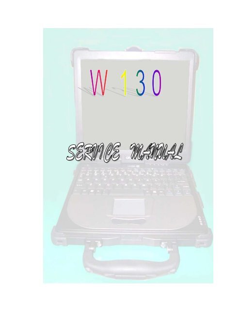
1 General system Description<br />
The LightNote W130 is a rugged and high portability industrial computer. The<br />
W130 also can connect with a docking to the capability of FLOPPY and<br />
CD-ROM and I/O device. The W130 model will support Intel Centrino mobile<br />
technology with Pentium-M Processors LV 1.1G, 1.2G with Micro-FCBGA,<br />
12W in TDP and 1Mb L2 Cache.<br />
This system is based on PCI architecture, which have standard hardware<br />
peripheral interface. The power management complies with Advanced<br />
Configuration and Power Interface (ACPI 2.0). It also prov<strong>id</strong>es easy<br />
configuration through CMOS setup, which is built in system BIOS software<br />
and can be pop-up by pressing F2 at system start up or warm reset.<br />
System also prov<strong>id</strong>es icon LEDs to display system status, such as Power<br />
indicator, HDD/CDROM, NUM LOCK, CAP LOCK, SCROLL LOCK,<br />
SUSPEND MODE and Battery charging status. It also one USB port.<br />
The memory subsystem supports One JEDEC-standard 200-pin, small-outline,<br />
dual in-line memory module (SODIMM), support PC2100 and up to 1GB DDR<br />
SDRAM.<br />
The W130 includes the 855GM chipset components GMCH and the ICH4-M.<br />
The Accelerated Hub Architecture interface (the chipset component<br />
interconnect) is designed into the chipset to prov<strong>id</strong>e an efficient, high<br />
bandw<strong>id</strong>th, communication channel between the GMCH and the ICH4-M.<br />
The GMCH component contains a processor system bus (PSB) controller, a<br />
graphics controller, and a memory controller, while prov<strong>id</strong>ing an LVDS<br />
interface and two DVO ports. The ICH4-M component integrates USB host<br />
controllers (supporting the USB 1.1 and USB 2.0 specification), an Ultra ATA<br />
100/66/33 controller, a LAN controller, and an AC’97 digital controller, while<br />
prov<strong>id</strong>ing interfaces for PCI and LPC devices,.<br />
To prov<strong>id</strong>e for the increasing number of mul<strong>tim</strong>edia applications, the AC97<br />
CODEC ALC201 is integrated onto the motherboard.<br />
5
A full set of software drivers and utilities are available to allow advanced<br />
operating systems such as Windows2000 and WindowsXP to take full<br />
advantage of the hardware capabilities such as bus mastering IDE,<br />
Windows2000-ready Plug & Play, and Advance configuration and power<br />
interface (ACPI 2.0).<br />
Following chapters will have more detail description for each indiv<strong>id</strong>ual<br />
sub-systems and functions.<br />
W130 System Diagram:<br />
D/D BD<br />
1:DC IN<br />
Primary Battery<br />
Keyboard<br />
Trace PAD<br />
Touch Screen 12.1” LCD/Touch Screen Inverter BD<br />
W130 Mother Board<br />
1:Intel Pentium-M LV 1.1G/1.2G<br />
2:One 200pin DDR SO-DIMM Socket (max: 1GB)<br />
3:USB*2, RS232*1 (COM1), Modem *1 (RJ-11), LAN*1 (RJ-45),VGA*1(DB15)<br />
4:PCMCIA*1(Type II)<br />
W1300 Docking Board<br />
1: USB*2, RS232*2(COM1.COM2), PIO PORT*1,PS2*1,CRT OUT*1<br />
2: MIC IN Con.*1,Line Out Con.*1,Mono Speaker*1<br />
3: FLOPPY*1,CD-ROM*1<br />
6
1.2 System Hardware Parts<br />
Internal Marketing Specifications<br />
CPU Intel Pentium M Processor LV1.1GHz in µ-FCBGA package<br />
FSB 400MHz<br />
CPU Thermal ceiling: 12W<br />
Core logic Intel 855GM Chipset + ICH4-M<br />
L2 Cache On-die 1MB L2 Cache<br />
System BIOS 512KB Flash EEPROM<br />
Includes System BIOS, VGA BIOS, plug & play, and ACPI 2.0<br />
capability<br />
Boot from IDE devices and LAN, USB CD-ROM<br />
Suspend to DRAM / HDD<br />
PC2001 compliance<br />
Memory One 200-pin PC2100 DDR SODIMM socket for memory<br />
expansion<br />
Supports 200MHz and 266MHz DDR devices<br />
Standard: 256MB Max: 1GB<br />
VGA 855GM integrate graphics controller<br />
Integrated 32-bit 3D/2D gfx core with Dynamic V<strong>id</strong>eo Memory<br />
Technology<br />
Support DirectX® 8.1<br />
Support AGP 4X<br />
Dual View function<br />
LCD/CRT simultaneous display capability<br />
V<strong>id</strong>eo Shared system memory 64MB<br />
Memory<br />
Display 12.1” TFT XGA (1024x768) LCD<br />
12.1” touch screen (Optional)<br />
Optional Sunlight Readable Panel (Transflective LCD)<br />
Structure 1-spindle<br />
HDD Standard: 40GB, Integrated, Support Ultra DMA-33/66/100<br />
2.5” 9.5mm height with damper protect<br />
Keyboard Water-proof membrane keyboard, Backlight function<br />
(Optional)<br />
Rubber keyboard with back-light (Optional)<br />
Pointing A touch-sensitive control pad with Microsoft Win Mouse<br />
Device function coexist<br />
PCMCIA Type II x 1 - Card Bus support<br />
Communicati 10/100 Base-T LAN<br />
on<br />
56K, V90. Modem<br />
802.11b Wireless LAN (Optional)<br />
(Supports Intel PRO/Wireless 2100 LAN mini-PCI type 3B<br />
adapter and Intel PROset software)<br />
Wireless Modem (DataTAC/PRM240 or GPRS/GSM or CDMA<br />
or IDEN(5mm)) (Optional)<br />
Audio AC97 <strong>au</strong>dio support<br />
7
MS-Sound compatible<br />
Built-in one speaker (Mono)<br />
Microphone-in<br />
Earphone-out<br />
I/O Port Serial port × 1<br />
VGA port x 1<br />
USB 2.0 port x 2<br />
DC input x1<br />
Docking Port x1<br />
RJ-11x1 for 56Kbps Software Modem port<br />
RJ-45 100 Base-T LAN port<br />
Microphone-in & Earphone out ports<br />
Battery - Support 9 cells Li-Ion Battery<br />
AC adapter - Universal AC adapter -Input: 100-240v, 50/60Hz AC.<br />
Dimensions 10.8” * 9.4” * 1.7” / 276mm * 239mm * 43mm<br />
Weight Goal is under 7.2 lbs<br />
Software Support Windows 2000 / Windows XP<br />
Environmental Standard (Main System)<br />
Temperature IEC 68-2-1,2,14 / MIL-STD-810F, Method 501.4, 502.4<br />
Operating: 0 o C to 50 o C<br />
-20 o C to 50 o C (Optional)<br />
Non-operating: -40 o C to 70 o C<br />
Hum<strong>id</strong>ity According to IEC 68-2-30 / MIL-STD-810F, Method 507.4<br />
5% to 95% RH, non-condensing<br />
Altitude According to IEC 68-2-13 / MIL-STD-810F, Method 500.4<br />
Operating: 15,000ft<br />
Non-operating: 40,000ft; altitude change rate: 2,000 ft/min<br />
Shock According to IEC 68-2-27 / MIL-STD-810F, Method 516.5<br />
Operating: 15g, 11 ms, half sine wave<br />
Non-operating: 50g, 11 ms, half sine wave<br />
Vibration According to IEC 68-2-6<br />
Sinuso<strong>id</strong>al wave vibration:<br />
Operating: 10~55Hz/0.075, 55~500Hz/1.0g<br />
Non-operating: 10~55Hz/0.15, 55~500Hz/2.0g<br />
Random vibration:<br />
MIL-STD-810F, 514.5 - high way truck vibration exposure<br />
Drop According to IEC 68-2-32 / MIL-STD-810F, Method 516.5<br />
3 Feet height free drop<br />
Test surface: steel plate<br />
ESD According to IEC1000-4-2<br />
Air Discharge:<br />
0KV~8KV(included), no any error<br />
8KV~15KV, allow soft error<br />
Contact Discharge:<br />
0KV~4KV(included), no any error<br />
4KV~ 8KV, allow soft error<br />
Enclosure According to IEC 529, MIL-STD-810F, IP 51<br />
Regulation FCC part 15, Subpart B, Class B, UL, CUL, TUV, Win key<br />
Options Removable Options:<br />
8
Docking board (Serial Port x2, USB2.0 x2, Parallel x1, VGA<br />
Port x1,<br />
DB26 (Male) x1)<br />
External Battery charger<br />
Factory Options:<br />
HDD heater for low temp. –4 o F (-20℃) to 122 o F (50℃)<br />
Membrane keyboard with backlight<br />
Rubber keyboard with backlight<br />
Wireless LAN (802.11b)<br />
Wireless Modem (DataTAC/PRM240 or GPRS/GSM or CDMA<br />
or IDEN (5mm))<br />
12.1” transflective LCD<br />
12.1” touch screen<br />
1.3 Major Component Introduction<br />
1.3.1 CPU Module<br />
Intel Pentium-M Processors with Micro-FCBGA package.<br />
The first Intel mobile processor with the Intel NetBurst micro-architecture<br />
which features include hyper-pipelined technology, a rap<strong>id</strong> execution<br />
engine, a 400MHz system, an execution trace cache, advanced dynamic<br />
execution, advanced transfer cache, enhanced floating point and<br />
multi-media unit, and Streaming SIMD Extensions 2 (SSE2).<br />
The Streaming SIMD Extensions 2 (SSE2) enable break-through levels of<br />
performance in mul<strong>tim</strong>edia applications including 3-D graphics, v<strong>id</strong>eo<br />
decoding/encoding, and speech recognition.<br />
Use Source-Synchronous Transfer (SST) of address and data to improve<br />
performance by transferring data four <strong>tim</strong>es per bus clock.<br />
Support Enhanced Intel SpeedStep technology, which enables real-<strong>tim</strong>e<br />
dynamic switching of the voltage and frequency between two performance<br />
modes.<br />
1.3.2 System frequency ICS950810<br />
Programmable output frequency, div<strong>id</strong>er ratios, output rise/fall <strong>tim</strong>e, output<br />
skew.<br />
Programmable spread percentage for EMI control.<br />
Watchdog <strong>tim</strong>er technology to reset system if system malfunctions.<br />
Programmable watchdog safe frequency.<br />
9
Support I2C Index read/write and block read/write operations.<br />
Use external 14.318MHz crystal.<br />
1.3.3 Intel 855-GM GMCH IGUI 3D Graphic DDR/SDR Chipset<br />
Intel 855-GM GMCH IGUI Host Memory Controller integrates a high<br />
performance host interface for Intel Banias processor, a high performance<br />
2D/3D Graphic Engine, a high performance memory controller, an AGP<br />
4X interface, and Intel®’ I/O Hub architecture INTEL 82801DBM ICH4-M.<br />
Intel 855-GM GMCH Host Interface features the AGTL & AGTL+<br />
compliant bus driver technology with integrated on-die termination to<br />
support Intel Pentium-M processors. 855-GM GMCH prov<strong>id</strong>es a 12-deep<br />
In-Order-Queue to support maximum outstanding transactions up to 12. It<br />
integrated a high performance 2D/3D Graphic Engine, V<strong>id</strong>eo Accelerator<br />
and Advanced Hardware Acceleration MPEGI/MPEGII V<strong>id</strong>eo Decoder for<br />
the Intel Pentium-M series based PC systems. It also integrates a high<br />
performance 2.1GB/s DDR266 Memory controller to sustain the<br />
bandw<strong>id</strong>th demand from the integrated GUI or external AGP master, host<br />
processor, as well as the multi I/O masters. In addition to integrated GUI,<br />
855-GM GMCH also can support external AGP slot with AGP 1X/2X/4X<br />
capability and Fast Write Transactions. A high bandw<strong>id</strong>th and mature<br />
Intel®’ I/O Hub architecture is incorporated to connect 855-GM GMCH<br />
and INTEL 82801DBM ICH4-Mtogether. Intel®’ I/O Hub architecture is<br />
developed into three layers, the Multi-threaded I/O Link Layer delivering<br />
1.2GB bandw<strong>id</strong>th to connect embedded DMA Master devices and external<br />
PCI masters to interface to Multi-threaded I/O Link layer, the<br />
Multi-threaded I/O Link Encoder/Decoder in INTEL 82801DBM ICH4-M to<br />
transfer data w/ 533 MB/s bandw<strong>id</strong>th from/to Multi-threaded I/O Link layer<br />
to/from 855-GM GMCH, and the Multi-threaded I/O Link Encoder/Decoder<br />
in 855-GM GMCH to transfer data w/ 533 MB/s from/to Multi-threaded I/O<br />
Link layer to/from INTEL 82801DBM ICH4-M.<br />
An Unified Memory Controller supporting DDR266 DRAM is incorporated,<br />
delivering a high performance data transfer to/from memory subsystem<br />
from/to the Host processor, the integrated graphic engine or external AGP<br />
master, or the I/O bus masters. The memory controller also supports the<br />
Suspend to RAM function by retaining the CKE# pins asserted in ACPI S3<br />
state in which only AUX source deliver power. The 855-GM GMCH adopts<br />
the Shared Memory Architecture, eliminating the need and thus the costs<br />
10
of the frame buffer memory by organizing the frame buffer in the system<br />
memory. The frame buffer size can be allocated from 8MB to 64MB.<br />
Features<br />
Processor/Host Bus Support<br />
Intel ® Pentium-M processor<br />
2X Address, 4X data<br />
Support host bus Dynamic Bus Inversion (DBI)<br />
Supports system bus at 400MT/s (100 MHz)<br />
Supports 64-bit host bus addressing<br />
8-deep In-Order-Queue<br />
AGTL+ bus driver technology with integrated GTL termination resistors<br />
and low voltage operation (1.05V)<br />
Supports Enhanced Intel® SpeedStepTM Technology (EIST) and<br />
Geyserville III<br />
Support for DPWR# signal to Pentium-M processor for PSB power<br />
management<br />
1.3.4 Memory System<br />
Directly supports one DDR channel, 64-bts w<strong>id</strong>e (72-b with ECC).<br />
Supports 200-MHz and 266-MHz DDR devices with unbuffered.<br />
PC1600/PC2100 DDR(with ECC).<br />
Supports 128-Mb, 256-Mb and 512-Mbit technologies prov<strong>id</strong>ing maximum<br />
capacity of 1-GB with only x 16 devices.<br />
All supported devices have 4 banks.<br />
Supports up to 16 simultaneous open pages.<br />
Supports page sizes of 2KB, 4KB, 8KB, and 16KB. Page size is<br />
indiv<strong>id</strong>ually selected for every row.<br />
UMA support only.<br />
1.3.5 Display<br />
Analog Display Support<br />
350 MHz integrated 24-bit RAMDAC that can drive a standard progressive<br />
scan analog monitor up to 1800x1350 @ 85 Hz.<br />
Accompanying I2C and DDC channels prov<strong>id</strong>ed through multiplexed<br />
interface Hotplug and display support<br />
Dual independent pipe with single display support Simultaneous: Same<br />
11
images and native display <strong>tim</strong>ings on each display device<br />
DVO (DVOB) support<br />
Digital v<strong>id</strong>eo out port DVOB with 165-MHz dot clock on 12-bit interface<br />
Variety of DVO devices channel<br />
Compliant with DVI Specification 1.0, thereby prov<strong>id</strong>ing support for a flat<br />
panel up to 2048x1536 pixel resolution, or digital CRT up to 1920x1080<br />
pixel resolution<br />
Dedicated LFP (local flat panel) interface<br />
Single or dual channel LVDS panel support up to SXGA+ panel resolution<br />
with frequency range from 25MHz to 112MHz per channel<br />
SSC support of 0.5%, 1.0%, and 2.5% center and down spread with<br />
external SSC clock<br />
Supports data format of 18 bpp<br />
LCD panel power sequencing compliant with SPWG <strong>tim</strong>ing specification<br />
Compliant with ANSI/TIA/EIA –644-1995 spec<br />
Integrated PWM interface for LCD backlight inverter control<br />
Bi-linear Panel fitting<br />
Tri-view support through LFP interface, DVO ports and CRT<br />
Internal Graphics Features<br />
Core Frequency<br />
Display Core frequency of 133MHz<br />
Render Core frequency of 133MHz<br />
2D Graphics Engine<br />
Op<strong>tim</strong>ized 128 bit BLT engine<br />
Ten programmable and predefined monochrome patterns<br />
Alpha Stretch Blt (via 3D pipeline)<br />
Anti-aliased lines<br />
Hardware-based BLT Clipping & Scissoring<br />
32-bit Alpha Blended cursor<br />
Programmable 64*64 3-color Transparent cursor<br />
Color Space Conversion<br />
3 Operand Raster BLTs<br />
8-bit, 16-bit, and 32-bit color<br />
ROP support<br />
DIB translation and Linear/Title addressing<br />
3D Graphics Engine<br />
3D Setup and Render Engine<br />
Viewpoint Transform and Perspective Div<strong>id</strong>e<br />
12
Triangle Lists, Strips and Fans support<br />
Indexed Vertex and Flexible Vertex formats<br />
Pixel accurate Fast Scissoring and Clipping operation<br />
Backface Culling support<br />
DirectX TM and OGL Pixelization rules<br />
Anti-Aliased Lines support<br />
Sprite Points support<br />
Zone Rendering<br />
Prov<strong>id</strong>es the highest sustained fill rate performance in 32-bit color and<br />
24-bit W mode<br />
High quality performance Texture Engine<br />
266 MegaTexel/speak performance<br />
Per Pixel Perspective corrected Texture Mapping<br />
Single Pass Texture Compositing (Multi-Texture) at rate<br />
Enhanced Texture Blending functions<br />
Twelve Level of Detail MIP Map Sizes from 1x1 to 2Kx2K<br />
Numerous Texture formats including 32-bit RGBA<br />
Alpha and Luminance Maps<br />
Texture Chromakeying<br />
Bilinear, Trilinear, Anisotropic MIP-Mapped Filtering<br />
Cubic Environment Reflection Mapping<br />
Embossed Bump-mapping<br />
DXTn Texture Decompression<br />
3D Graphics Rasterrization enhancements<br />
One Pixel per Clock<br />
Flat and Gour<strong>au</strong>d Shading<br />
Color Alpha Blending for Transparency<br />
Vertex and Programmable Pixel Fog and Atmospheric effects<br />
Color Specular Lighting<br />
Vertex and Programmable Pixel Fog and Atmospheric effects<br />
Z Bais support<br />
Dithering<br />
Line and Full-Scence Anti-Aliasing<br />
16 and 24-bit Z Buffering<br />
16 and 24-bit W Buffering<br />
8-bit Stencil Buffering<br />
Double and Triple Render Buffer support<br />
16 and 32 –bit color<br />
13
Destination Alpha<br />
Vertex Cahec<br />
Maximum 3D resolution of 1600x1200 x32 bpp at 85 Hz<br />
Op<strong>tim</strong>al 3D resolution supported<br />
Fast Clear support<br />
ROP support<br />
1.3.6 HUB Interface for ICH4<br />
266 MB/s point to point hub interface to ICH4-M<br />
66-M Hz base clock<br />
Supports the following traffic types to the ICH4-M<br />
Hub interface-to DRAM<br />
CPU-to-Hub interface<br />
Messaging<br />
MSI interrupt messages<br />
Power Management state change<br />
SMI, SCI, and SERR error indication<br />
Power Management<br />
SMRAM space remapping to A0000h (128-KB)<br />
Supports extended SMRAM space above 256- MB ,additional 1 MB TSEG<br />
from top of Memory, cacheable (cacheability controlled by CPU)<br />
APM rev 1.2 compliant power management<br />
Supports Suspend to System Memory(S3),Suspend to Disk(S4) and Hard<br />
Off/Total Reboot(S5)<br />
ACPI 1.0b 2.0 Support<br />
1.3.7 I/O Controller Hub: INTEL 82801DBM<br />
The INTEL 82801DBM ICH4-M integrates three Universal Serial Bus 2.0<br />
Host Controllers, the Audio Controller with AC 97 Interface, the IDE<br />
Master/Slave controllers, and Intel®’ I/O Hub architecture. The PCI to LPC<br />
Br<strong>id</strong>ge, I/O Advanced Programmable Interrupt Controller, legacy system<br />
I/O and legacy power management functionalities are integrated as well.<br />
The integrated Universal Serial Bus Host Controllers features Dual<br />
Independent UHCI Compliant Host controllers with six USB ports<br />
delivering 480 Mb/s bandw<strong>id</strong>th and rich connectivity. Bes<strong>id</strong>es, Legacy<br />
USB devices as well as over current detection are also implemented.<br />
14
The Integrated AC97 v2.3 compliance Audio Controller that features a<br />
7-channels of <strong>au</strong>dio speaker out and HSP v.90 modem support.<br />
Additionally, the AC97 interface supports 4 separate SDATAIN pins that is<br />
capable of supporting multiple <strong>au</strong>dio code with one separate modem<br />
code.<br />
The integrated IDE Master/Slave controllers features Dual Independent<br />
IDE channels supporting PIO mode transfers up to 16 Mbytes/sec and<br />
Ultra DMA 33/66/100. It prov<strong>id</strong>es two separate data paths for the dual IDE<br />
channels that sustain the high data transfer rate in the multitasking<br />
environment.<br />
INTEL 82801DBM ICH4-M supports 6 PCI masters and complies with PCI<br />
2.2 specification. It also incorporates the legacy system I/O like: two<br />
82C37 compatible DMA controllers, Channels 0-3 are hardwired to 8 bit,<br />
three 8254 compatible programmable 16-bit counters channels 5-7,<br />
hardwired keyboard controller and PS2 mouse interface(not use in MiTAC<br />
8080 model), Real Time clock with 512Bytes CMOS SRAM and two<br />
82C59 compatible Interrupt controllers. Bes<strong>id</strong>es, the I/O APIC managing<br />
up to 14 interrupts with both Serial and FSB interrupt delivery modes is<br />
supported.<br />
The integrated power management module incorporates the ACPI 1.0b<br />
compliance functions, the APM 1.2 compliance functions, and the PCI bus<br />
power management interface spec. v1.1. Numerous power-up events and<br />
power down events are also supported. 21 general purposed I/O pins are<br />
prov<strong>id</strong>ed to give an easy to use logic for specific application. In addition,<br />
the INTEL 82801DBM ICH4-M supports Deeper Sleep power state for<br />
Intel Mobile processor.<br />
A high bandw<strong>id</strong>th and mature Intel®’ I/O Hub architecture is incorporated<br />
to connect Montara and Intel 82801DBM ICH4-M Hub interface together.<br />
Intel®’ I/O Hub architecture is developed<br />
Features<br />
PCI Bus Interface<br />
Supports PCI Revision 2.2 Specification at 33 MHz<br />
133 MB/sec maximum throughput<br />
Supports up to six master devices on PCI<br />
One PCI REQ/GNT pair can be given higher arbitration priority (intended<br />
for external 1394 host controller)<br />
Support for 44-bit addressing on PCI using DAC protocol Integrated<br />
LAN Controller<br />
15
WfM 2.0 and IEEE 802.3 compliant<br />
LAN Connect Interface (LCI)<br />
10/100 Mbit/sec Ethernet support_ Integrated IDE Controller<br />
Supports “Native Mode” register and interrupts<br />
Independent <strong>tim</strong>ing of up to 4 drives, with separate primary and secondary<br />
IDE cable connections<br />
Ultra ATA/100/66/33, BMIDE and PIO modes<br />
Tri-state modes to enable swap bay<br />
USB<br />
Includes three UHCI host controllers that support six external ports<br />
New: Includes one EHCI high-speed USB 2.0 Host Controller that<br />
supports all six ports<br />
New: Supports a USB 2.0 high-speed debug port<br />
Supports wake-up from sleeping states S1–S5<br />
Supports legacy keyboard/mouse software AC-Link for Audio and<br />
Telephony CODECs<br />
Supports AC ’97 2.3<br />
New: Third AC_SDATA_IN line for three code support<br />
New: Independent bus master logic for seven channels (PCM In/Out, Mic<br />
1 input, Mic 2 input, modem in/out, S/PDIF out)<br />
Separate independent PCI functions for <strong>au</strong>dio and modem<br />
Support for up to six channels of PCM <strong>au</strong>dio output (full AC3 decode)<br />
Supports wake-up events Interrupt Controller<br />
Support up to eight PCI interrupt pins<br />
Supports PCI 2.2 message signaled interrupts<br />
Two cascaded 82C59 with 15 interrupts<br />
Integrated I/O APIC capability with 24 interrupts<br />
Supports serial interrupt protocol<br />
Supports processor system bus interrupt delivery New: 1.5 V operation<br />
with 3.3 V I/O<br />
5 V tolerant buffers on IDE, PCI, USB overcurrent and legacy signals<br />
Timers Based on 82C54<br />
System <strong>tim</strong>er, refresh request, speaker tone output Power Management<br />
Logic<br />
ACPI 2.0 compliant<br />
ACPI-defined power states (C1–C2, S3–S5 )<br />
Supports Desktop S1 state (like C2 state, only STPCLK# active)<br />
ACPI power management <strong>tim</strong>er<br />
16
PCI PME# support<br />
SMI# generation<br />
All registers readable/restorable for proper resume from 0 V suspend<br />
states External Glue Integration<br />
Integrated pull-up, pull-down and series termination resistors on IDE,<br />
processor interface<br />
Integrated Pull-down and Series resistors on<br />
1.3.8 Super I/O_NS PC87393<br />
National Semiconductor’s PC8739x family of LPC Super I/O devices is<br />
targeted for a w<strong>id</strong>e range of portable applications. PC99 and ACPI<br />
compliant, the PC8739x family features an X-Bus Extension for read and<br />
write operations over the X-Bus, a full IEEE 1284 Parallel Port with a<br />
Parallel Port Multiplexer (PPM) for external Floppy Disk Drive (FDD)<br />
support, a Musical Instrument Digital Interface (MIDI) port, and a Game<br />
port. Like all National LPC Super I/O devices, the PC8739x offers a<br />
single-chip solution to the most commonly used PC I/O peripherals.<br />
The PC8739x family also incorporates: a Floppy Disk Controller (FDC),<br />
two enhanced Serial Ports (UARTs), one with Fast Infrared (FIR, IrDA 1.1<br />
compliant), General-Purpose Input/Output (GPIO) support for a total of 32<br />
ports, Interrupt Serializer for Parallel IRQs and an enhanced WATCH<br />
DOG <strong>tim</strong>er.<br />
1.3.9 Keyboard controller Hitachi H8/3437<br />
The H8/3437 Series is a series of high-performance microcontrollers with<br />
a fast H8/300 CPU core and a set of on-chip supporting functions<br />
op<strong>tim</strong>ized for embedded control. These include ROM, RAM, four types of<br />
<strong>tim</strong>ers, a serial communication interface, optional I2C bus interface, host<br />
interface, A/D converter, D/A converter, I/O ports, and other functions<br />
needed in control system configurations, so that compact,<br />
high-performance systems can be implemented easily. The series<br />
includes the H8/3437 with 60-kbyte ROM and 2-kbyte RAM, the H8/3436<br />
with 48-kbyte ROM and 2-kbyte RAM, and the H8/3434 with 32-kbyte<br />
ROM and 1-kbyte RAM.<br />
The H8/3437, H8/3436, and H8/3434 are available in mask-ROM versions.<br />
The H8/3437 and H8/3434 are also available in ZTAT*1 (zero<br />
turn-around <strong>tim</strong>e) versions, prov<strong>id</strong>ing a quick and flexible response to<br />
17
conditions from ramp-up through full-scale volume production, even for<br />
applications with frequently changing specifications. In addition, the<br />
H8/3434 and H8/3437 have F-ZTAT*2 (flexible-ZTAT) versions with<br />
on-board programmability.<br />
1.3.10 Fax/Modem module<br />
The PCT2303W chipset is designed to meet the demand of this emerging<br />
worldw<strong>id</strong>e AMR/MDC market. The combination of PC-TEL’s well proven<br />
PCT2303W chipset and the HSP56TM MR software modem driver allows<br />
systems manufactures to implement modem functions in PCs at a lower bill of<br />
materials (BOM) while maintaining higher system performance.<br />
PC-TEL has streamlined the traditional modem into the Host Signal<br />
Processing (HSP) solution. Operating with the Pentium class processors, HSP<br />
becomes part of the host computer’s system software. It requires less power<br />
to operate and less physical space than standard modem solutions. PC-TEL’s<br />
HSP modem is an easily integrated, cost-effective communications solution<br />
that is flexible enough to carry you into the future.<br />
The PCT2303W chip set is an integrated direct access arrangement (DAA)<br />
and Codec that prov<strong>id</strong>es a programmable line interface to meet international<br />
telephone line requirements. The PCT2303W chip set is available in two<br />
16-pin small outline packages (AC’97 interface on PCT303A and phone-line<br />
interface on PCT303W). The chip set eliminates the need for an AFE, an<br />
isolation transformer, relays, opto-isolators, and 2-to 4-wire hybr<strong>id</strong>. The<br />
PCT2303W chip set dramatically reduces the number of discrete components<br />
and cost required to achieve compliance with international regulatory<br />
requirements. The PCT2303W complies with AC’97 Interface specification<br />
Rev. 2.1. The chip set is fully programmable to meet worldw<strong>id</strong>e telephone line<br />
interface requirements including those described by CTR21, NET4, JATE,<br />
FCC, and various country-specific PTT specifications. The programmable<br />
parameters of the PCT2303W chip set include AC termination, DC termination,<br />
ringer impedance, and ringer threshold. The PCT2303W chip set has been<br />
designed to meet stringent worldw<strong>id</strong>e requirements for out-of-band energy,<br />
billing-tone immunity, lightning surges, and safety requirements<br />
1.3.11 FAST ETHERNET CONTROLLER integrated ICH-4M<br />
18
Built-in ICH-4M<br />
Use INTEL 82562ET highly integrated platform LAN connect devices<br />
combining 10base-t and 100base-tx physical layer capabilities.<br />
1.3.12 PCMCIA controller_ ENE CB1410 + ENE CP2211<br />
CP2211 is a single slot PCMCIA and CardBus power switch. It integrates<br />
control logic, low switching resistance MOSFET, over current alarm and<br />
over temperature <strong>au</strong>to shutdown circuits. It can deliver 3.3V or 5V to PC<br />
Card xVCCOUT and 3.3V, 5V or 12V to PC Card xVPPOUT. The output<br />
current is up to 1A for xVCCOUT and 250mA for xVPPOUT. The power is<br />
controlled by 4-wire parallel data interface VCCD0Z, VCCD1Z, VPPD0<br />
and VPPD1.<br />
Low Switching Resistance (100mΩ for VCC Switch)<br />
Over current alarm via OC#<br />
Over temperature <strong>au</strong>to shutdown<br />
1A output current for xVCCOUT<br />
150mA output current for xVPPOUT<br />
Only 3.3V is required for chip normal operation<br />
12V is not required for 3.3V or 5V Output<br />
Break-Before-Mask Switching<br />
16-Pin SSOP Package (209 mil)<br />
1.3.13 AC”97 Code ALC202<br />
Single chip <strong>au</strong>dio CODEC with high S/N ratio (>90dB)<br />
Compliant with AC’97 2.2 & WHQL specifications<br />
Support of S/PDIF out is compliant with AC’97 rev2.2 specifications<br />
Meets performance requirements for <strong>au</strong>dio on PC2001 systems<br />
Meets Microsoft PC99 & WLP 2.0 <strong>au</strong>dio requirements<br />
18-bit Stereo full-duplex CODEC with independent and variable sampling<br />
rate<br />
18-bit ADC and 20-bit DAC resolution<br />
Four analog line-level stereo inputs with 5-bit volume control: LINE_IN,<br />
CD, IDEO, AUX<br />
High quality differential CD input Two analog line-level mono input:<br />
PC_BEEP,PHONE_IN<br />
19
Supports double sampling rate (96KHz) of DVD <strong>au</strong>dio playback<br />
Two software selectable MIC inputs +30dB boost preamplifier for MIC<br />
input<br />
Stereo output with 6-bit volume control Mono output with 5-bit volume<br />
control<br />
Headphone output with 50mW/8. driving capability (ALC202)<br />
Line output with 50mW/8. driving capability<br />
(ALC202A) Headphone jack-detect function to mute LINE/MONO/HP<br />
output, and to control S/PDIF output<br />
3D Stereo Enhancement<br />
Multiple CODEC extension capability<br />
External Amplifier Power Down (EAPD) capability<br />
High performance converter technology<br />
Power management and enhanced power saving<br />
2 GPIO pins<br />
No external crystal/clock required<br />
14.318MHz 24.576MHz PLL saves crystal<br />
DC Voltage volume control<br />
Auxiliary power (VAUX ) to support Power Off<br />
CD function<br />
Power support: Digital: 3.3V; Analog: 3.3V/5V<br />
Standard 48-Pin LQFP Package<br />
1.3.14 Thermal sensor_ ADM1021A<br />
On-Chip and Remote Temperature Sensing<br />
No Calibration Necessary<br />
1_C Accuracy for On-Chip Sensor<br />
3_C Accuracy for Remote Sensor<br />
Programmable Over/Under Temperature Limits<br />
Programmable Conversion Rate<br />
2-Wire SMBus Serial Interface<br />
Supports System Management Bus (SMBus) Alert<br />
200 _A Max Operating Current<br />
1 _A Standby Current<br />
3 V to 5.5 V Supply<br />
Small 16-Lead QSOP Package<br />
20
2 Motherboard Function Description<br />
2.1 Hot Key Function<br />
Keys<br />
Combinatio<br />
n<br />
Feature Meaning<br />
Fn + F1 Reserve<br />
Fn + F2 Reserve<br />
Fn + F3 Volume Down<br />
Fn + F4 Volume Up<br />
Fn + F5 Brightness Down Decreases LCD brightness<br />
Fn + F6 Brightness Up Increases LCD brightness<br />
Fn + F7 Reserve<br />
Fn + F8 LCD On/Off Toggle LCD On or Off<br />
Fn + F9<br />
LCD/CRT<br />
Switching<br />
Switch display mode of LCD only, CRT only, and<br />
simultaneously display.<br />
Force system into either Suspend to DRAM (S3)<br />
Fn + F10 Suspend or Suspend to HDD (S4) mode based on BIOS<br />
Setting<br />
2.2 Power on/off/suspend/resume button<br />
APM mode<br />
At APM mode, Power button is on/off system power.<br />
ACPI mode<br />
At ACPI mode. Windows power management control panel set power button<br />
behavior.<br />
You could set “standby”, “power off” or “hibernate”(must enable hibernate<br />
function in power<br />
Management) to power button function.<br />
Continue pushing power button over 4 seconds will force system off at ACPI<br />
mode.<br />
21
2.3 Cover Switch<br />
System <strong>au</strong>tomatically prov<strong>id</strong>es power saving by monitoring Cover Switch. It<br />
will save battery power and prolong the usage <strong>tim</strong>e when user closes the<br />
notebook cover.<br />
At ACPI mode there are four functions to be chosen at windows power<br />
management control panel.<br />
None<br />
Standby<br />
Off<br />
Hibernate (must enable hibernate function in power management)<br />
2.4 LED Indicators<br />
ON M/B LED:<br />
D21 -> HDD/CD-ROM/FLOPPY Active LED (orange).<br />
D17 -> LAN detect and active LED (100M – green, 10M- orange).<br />
D12 -> SCROLL LOCK LED (green).<br />
D15 -> NUM LOCK LED (green).<br />
D16-> CAPS LOCK LED (green).<br />
SIDE LED:<br />
D12 -> Adapter in LED (green).<br />
D10 -> Battery states LED.<br />
Ac in and Power on -> (Charge ok – green, Charging – orange, Battery<br />
dead – LED Dark).<br />
Ac in and Power off -> (Charge ok –Led dark, Charging – orange).<br />
D11 ->POWER/SUSPEND States LED (Power on – green, Suspend –<br />
orange)<br />
D13 -> Battery LOW (orange).<br />
22
2.5 Battery status<br />
Battery Warning<br />
System also prov<strong>id</strong>es Battery capacity monitoring and gives user a<br />
warning so that user has chance to save his data before battery dead.<br />
Also, this function protects system from mal-function while battery<br />
capacity is low.<br />
Battery Warning: Capacity below 10%, Battery Capacity LED flashes per<br />
second, system beeps per 2 seconds.<br />
System will suspend to HDD after 2 Minutes to protect user data.<br />
Battery Low State<br />
After Battery Warning State, and battery capacity is below 4%, system will<br />
generate beep for twice per second.<br />
Battery Dead State<br />
When the battery voltage level reaches 9.32 volts, system will shut down<br />
<strong>au</strong>tomatically in order to extend the battery packs' life.<br />
2.6 CMOS Battery<br />
CR2032 3V 220mAh lithium battery<br />
When AC in or system main battery ins<strong>id</strong>e, CMOS battery will consume<br />
no power.<br />
AC or main battery not exists, CMOS battery life at less (220mAh/5.8uA)<br />
4 years.<br />
Battery was put in battery holder, can be replaced.<br />
2.7 I/O Port<br />
I/O Port – USB #1<br />
23
One USB 2.0 Port<br />
Supports UHCI Design Gu<strong>id</strong>e<br />
Connector: Foxconn UB5112C-S1, 4 pin SMT type, male, R/A & Shroud<br />
connector<br />
Power supply for device: 5Vdc, 0.5Amp.<br />
Support USB FDD Boot up function.<br />
Microphone Input Jack<br />
Mono input.<br />
Input Voltage: 1 Vrms max.<br />
Connector : SMK LGY2313-0200,ψ 3.5MM<br />
Earphone Output Jack<br />
Stereo output, 200mW maximum.<br />
Allow Load Impedance = Min. 8Ω .<br />
Connector : Sharp GP1F562T,ψ 3.5MM, with Optic transmitter.<br />
I/O Port - RS232 COM1<br />
Connector: SUYIN 7321P-09G2, 9 pins D-SUB Connector, male, R/A type.<br />
RS232 Buffer: Analog Device ADM3311ARU.<br />
D/C Input<br />
Connector: 伸銘 955-853, 3- pin Power jack connector.<br />
PCMCIA Socket<br />
Single slot, support one type-II PC Card.<br />
Socket Type: Bottom S<strong>id</strong>e of PCB.<br />
Card type: R2 or Card bus support.<br />
24
RJ-11 Fax/Modem Port<br />
56 kbps data rate.<br />
Support telephone answering machine (TAM) function.<br />
Support V.90 function via software.<br />
Support power down (sleep) mode.<br />
One RJ-11 phone jack output.<br />
Docking Interface<br />
Interface included: USB*2, COM1/2, CRT, PIO, PS/2, Microphone, Earphone,<br />
IDE and FDD.<br />
Connector: BERG 91294-002, MICROPAX SMT 160 pins plug connector.<br />
Mating connector: BERG 91403-002, 0.25mm MICROPAX SMT 160 pins<br />
receipt connector.<br />
Contact life: 2500 <strong>tim</strong>es guaranteed.<br />
Touch Screen Pen<br />
Material & Color: plastic, black.<br />
Structure: 3 segments, length expansible from 75~130 ±3mm.<br />
25
3.1 LCD PANEL<br />
3 Peripheral<br />
Support 12.1” TFT XGA LCD display, Resolution up to XVGA (1024*768),<br />
18-bit color.<br />
Brightness: 100 ±10 lux<br />
Interface: LVDS<br />
3.2 HDD<br />
Toshiba 40GB<br />
Height: 9.5 mm, 2.5”<br />
3.3 Keyboard<br />
Windows 82 Keyboard, 1 color, multi languages support, US and Europe<br />
Keyboard<br />
3.4 Track Pad Synaptic<br />
Accurate positioning<br />
Low fatigue pointing action<br />
Low profile<br />
No moving part, high reliability<br />
Low power consumption<br />
Environmentally sealed<br />
Compact size.<br />
Software configurable<br />
Low weight<br />
Operating hum<strong>id</strong>ity: 5%-95% relative hum<strong>id</strong>ity, non condensing<br />
Storage temperature: -40 to +65 degree C<br />
26
ESD: 15KV applied to front surface<br />
Power supply voltage: 5.0Voltage ± 10%<br />
Power supply current: 4.0mA max operating.<br />
3.5 Memory<br />
DDR-RAM/ATP//128M/256M<br />
DDR-RAM/Apacer//128M/256M<br />
DDR-RAM/Un<strong>id</strong>orsa//128M/256M<br />
3.6 Modem MDC<br />
Askey<br />
27
4 Power Management<br />
The Tetra system has built in several powers saving modes to prolong the<br />
battery usage. User can enable and configure different degrees of power<br />
management modes via ROM CMOS setup (booting by pressing F2 key).<br />
Following are the descriptions of the power management modes supported.<br />
4.1 System Management Mode<br />
Full on mode<br />
In this mode, each device is running with the maximal speed. CPU clock is up<br />
to its maximum.<br />
Doze Mode<br />
In this mode, CPU will be toggling between on & stop grant mode either. The<br />
technology is clock throttling. This can save battery power without loosing<br />
much computing capability.<br />
The CPU power consumption and temperature is lower in this mode.<br />
Standby mode<br />
For more power saving, it turns of the peripheral components. In this mode,<br />
the following is the status of each device:<br />
--CPU: Stop grant<br />
--LCD: backlight off<br />
--HDD: spin down<br />
Suspend to DRAM<br />
The most chipset of the system is entering power down mode for more power<br />
saving. In this mode, the following is the status of each device:<br />
CPU: off<br />
Twister K: Partial off<br />
28
VGA: Suspend<br />
PCMCIA: Suspend<br />
Audio: off<br />
SDRAM: self refresh<br />
Suspend to HDD<br />
All devices are stopped clock and power-down<br />
System status is saved in HDD<br />
All system status will be restored when powered on again<br />
4.2 Battery Life<br />
Power Consumption & Battery Lift<br />
Battery Watts Test program Full Run Battery Life<br />
Primary 66.6WHr Battery Mark4.01 Around 150 minutes<br />
Battery Life of -20℃ ambient (Optional)<br />
Battery Watts Test program Full Run Battery Life<br />
Primary 66.6WHr Battery Mark4.01<br />
At least 90 minutes (charge above<br />
25℃, discharge at -20℃)<br />
The maximum battery capacity on -20degrees C is 60% of 25 degrees C.<br />
4.3 Other power management functions<br />
HDD & V<strong>id</strong>eo access<br />
System has the ability to monitor v<strong>id</strong>eo and hard disk activity. User can enable<br />
monitoring function for v<strong>id</strong>eo and/or hard disk indiv<strong>id</strong>ually. When there is no<br />
v<strong>id</strong>eo and/or hard disk activity, system will enter next PMU State depending on<br />
the application. When the VGA activity monitoring is enabled, the performance<br />
of the system will have some impact.<br />
29
5 Connector and Switch Definition<br />
Table 5-1 D/D Board Connector (J3) Pin Assignments<br />
Pin Name Pin No Description<br />
VDOCK 1,3,5,7<br />
AC Adapter input(From Docking BD to D/D BD), 19Vdc, max. 3.16A<br />
input.<br />
VMAIN 19,21,23,25<br />
CPU Vdc, Max. 25W Output, +12.6~+19Vdc, Ripple & Noise below<br />
1%.<br />
VDD5 35 Uninterrupt +5Vdc, Max. 100mA, +4.75~+5.25Vdc<br />
+12V 37<br />
+12Vdc, Max. 120mA Output, +11.4~+12.6Vdc, Ripple & Noise below<br />
1%.<br />
+5V 27,29,31,33 +5Vdc, Max. 3A Output, +4.75~+5.25Vdc, Ripple & Noise below 1%.<br />
+3V 9,11,13,15,17<br />
+3Vdc, Max. 3A Output, +3.135~+3.465Vdc, Ripple & Noise below<br />
1%.<br />
BAT_TEST 49 TEST Battery on boot to charge and discharge states<br />
DC_IN 43 AC adapter input power present, HI active, TTL output.<br />
D/BAT/CHG# 47 Detect Battery charge states<br />
BAT_DEAD 45<br />
Primary Battery Power reach to Dead level, (Battery power can’t keep<br />
the 12/5/3V output). High active, TTL output.<br />
VBAT 41<br />
Reflect the current Primary Battery Voltage for host Primary Battery<br />
low detects.<br />
SMC_H8 44<br />
Smart battery clock signal of Primary Battery, pass from Primary<br />
Battery.<br />
SMD_H8 46<br />
Smart battery data signal of Primary Battery, pass from Primary<br />
Battery.<br />
PWR_ON 48 Turn on +12/+5/+3Vdc output, high active, TTL output.<br />
POWERBTN# 50 Power Button Signal,Low avtive.<br />
KBGPIO1,2 39,40 KB Backlight control GPIO pin<br />
GND<br />
2,4,6,8,10,12,14,16<br />
,18,20,22,24,26,28<br />
,30,32,34,36,38,40<br />
Ground<br />
Table 5-2 HD Connector (J501) Pin Assignment<br />
Pin Name Pin No Description<br />
IDEPD0 17 IDE Device data 0<br />
IDEPD1 15 IDE Device data 1<br />
IDEPD2 13 IDE Device data 2<br />
IDEPD3 11 IDE Device data 3<br />
IDEPD4 9 IDE Device data 4<br />
IDEPD5 7 IDE Device data 5<br />
IDEPD6 5 IDE Device data 6<br />
IDEPD7 3 IDE Device data 7<br />
IDEPD8 4 IDE Device data 8<br />
IDEPD9 6 IDE Device data 9<br />
IDEPD10 8 IDE Device data 10<br />
IDEPD11 10 IDE Device data 11<br />
IDEPD12 12 IDE Device data 12<br />
IDEPD13 14 IDE Device data 13<br />
30
IDEPD14 16 IDE Device data 14<br />
IDEPD15 18 IDE Device data 15<br />
IDE_RST# 1 IDE Reset signal<br />
PDREQ 21 IDE Device DMA Request<br />
PIOW# 23 Disk I/O Write<br />
PIOR# 25 Disk I/O Read<br />
PIORDY 27 I/O Channel Ready<br />
PCSEL 28 Cable Select<br />
PDACK# 29 IDE Device DMA Acknowledge<br />
PIRQ14 31 Interrupt Requests 14<br />
PIOCS16# 32 16-BIT I/O Chip Select<br />
IDEPA0 35 IDE Device Address 0<br />
IDEPA1 33 IDE Device Address 1<br />
IDEPA2 36 IDE Device Address 2<br />
IDEPDIAG 34 Passed Diagnostic<br />
PCS#1 37 IDE Device Chip Select for 100 Range<br />
PCS#3 38 IDE Device Chip Select for 300 Range<br />
HD/CD_LED 39 HDD AND CD ROM Active LED<br />
HDD_+5V 41,42 HDD POWER<br />
GND<br />
2,19,22,24,26,30,40,<br />
43<br />
Ground<br />
Table 5-3 PCMCIA Connector (J7) Pin Assignment<br />
Pin Name Pin No Description<br />
CAD0 2 CardBus address/data bus<br />
CAD1 3 CardBus address/data bus<br />
CAD2 37 CardBus address/data bus<br />
CAD3 4 CardBus address/data bus<br />
CAD4 38 CardBus address/data bus<br />
CAD5 5 CardBus address/data bus<br />
CAD6 39 CardBus address/data bus<br />
CAD7 6 CardBus address/data bus<br />
CAD8 41 CardBus address/data bus<br />
CAD9 8 CardBus address/data bus<br />
CAD10 42 CardBus address/data bus<br />
CAD11 9 CardBus address/data bus<br />
CAD12 10 CardBus address/data bus<br />
CAD13 44 CardBus address/data bus<br />
CAD14 11 CardBus address/data bus<br />
CAD15 45 CardBus address/data bus<br />
CAD16 46 CardBus address/data bus<br />
CAD17 55 CardBus address/data bus<br />
CAD18 22 CardBus address/data bus<br />
31
CAD19 56 CardBus address/data bus<br />
CAD20 23 CardBus address/data bus<br />
CAD21 24 CardBus address/data bus<br />
CAD22 25 CardBus address/data bus<br />
CAD23 26 CardBus address/data bus<br />
CAD24 27 CardBus address/data bus<br />
CAD25 28 CardBus address/data bus<br />
CAD26 29 CardBus address/data bus<br />
CAD27 30 CardBus address/data bus<br />
CAD28 64 CardBus address/data bus<br />
CAD29 31 CardBus address/data bus<br />
CAD30 65 CardBus address/data bus<br />
CAD31 66 CardBus address/data bus<br />
CC/BE0# 7 CardBus bus commands and byte enables.<br />
CC/BE1# 12 CardBus bus commands and byte enables.<br />
CC/BE2# 21 CardBus bus commands and byte enables.<br />
CC/BE3# 61 CardBus bus commands and byte enables.<br />
CPAR 13 CardBus bus parity<br />
CPERR# 14 CardBus parity error indicator<br />
CGNT# 15 CardBusI bus grrant<br />
CINT# 16 CardBus interrupt<br />
CIRDY# 20 CardBus initiator ready<br />
CCLKRUN# 33 CardBus clock run<br />
CCD1# 36 CardBus datect 1<br />
CVS1,CVS2 43,57 CarsBus voltage sense 1 and CardBus datect 2<br />
CBLOCK# 48 CardBus lock<br />
CSTOP# 49 CarsBus stop<br />
CDEVSEL# 50 CardBus device select<br />
CTRDY# 53 CardBus target ready<br />
CFRAME# 54 CardBus cycle frame<br />
CRST# 58 CardBus reset<br />
CSERR# 59 CardBus system error<br />
CREQ# 60 CradBus request<br />
CAUDIO 62 CardBus <strong>au</strong>dio<br />
CSTSCHG 63 CradBus states change<br />
CCD2# 67 CardBus datect 1<br />
CCLK 19 CardBus clock<br />
CARD_VCC 17,51<br />
Switched output that delivers 0 V, 3.3-V, 5-V, or high impedance to<br />
card<br />
VPPOUT 18,52<br />
Switched output that delivers 0 V 3.3-V, 5-V, 12-V, or high impedance<br />
to card<br />
GND 1,34,35,68 Ground<br />
32
Wireless Modem Connector (J8,J10)<br />
Table 5-4 Keyboard Connector (J5) Pin Assignment<br />
Pin Name Pin No Description<br />
KI0 8 Keyboard Matrix Scan Input Line 0<br />
KI1 7 Keyboard Matrix Scan Input Line 1<br />
KI2 6 Keyboard Matrix Scan Input Line 2<br />
KI3 5 Keyboard Matrix Scan Input Line 3<br />
KI4 4 Keyboard Matrix Scan Input Line 4<br />
KI5 3 Keyboard Matrix Scan Input Line 5<br />
KI6 2 Keyboard Matrix Scan Input Line 6<br />
KI7 1 Keyboard Matrix Scan Input Line 7<br />
KO0 9 Keyboard Matrix Scan Output Line 0<br />
KO1 10 Keyboard Matrix Scan Output Line 1<br />
KO2 22 Keyboard Matrix Scan Output Line 2<br />
KO3 11 Keyboard Matrix Scan Output Line 3<br />
KO4 12 Keyboard Matrix Scan Output Line 4<br />
KO5 16 Keyboard Matrix Scan Output Line 5<br />
KO6 13 Keyboard Matrix Scan Output Line 6<br />
KO7 15 Keyboard Matrix Scan Output Line 7<br />
KO8 20 Keyboard Matrix Scan Output Line 8<br />
KO9 17 Keyboard Matrix Scan Output Line 9<br />
KO10 18 Keyboard Matrix Scan Output Line 10<br />
KO11 14 Keyboard Matrix Scan Output Line 11<br />
KO12 19 Keyboard Matrix Scan Output Line 12<br />
KO13 21 Keyboard Matrix Scan Output Line 13<br />
KO14 23 Keyboard Matrix Scan Output Line 14<br />
KO15 24 Keyboard Matrix Scan Output Line 15<br />
Table 5-5 CMOS Connector (J512) Pin Assignment<br />
Pin Name Pin No Description<br />
VCC_RTC 1 CMOS POWER<br />
GND 2 Ground<br />
Table 5-6 MONO SPEAKER Connector (J507) Pin Assignment<br />
Pin Name Pin No Description<br />
SPEAKER+ 1 Speaker + Signal<br />
SPEAKER- 2 Speaker - Signal<br />
33
Table 5-7 MDC TRANSFER BD Connector (J509) Pin Assignment<br />
Pin Name Pin No Description<br />
MONO_OUT 1 AC’97 Audio Mono Output<br />
AC97_SDOUT 23 AC’97 Serial Data Out<br />
AC97_RESET# 25 AC’97 Reset<br />
MODEM_SPK 4 Modem Speaker Signal<br />
AC97_SYNC 22 AC’97 Sync.<br />
AC97_SDIN1 24 AC’97 Serial Data In<br />
AC97_BITCLK 30 AC’97 Bit Clock<br />
+3V 17,21 +3V Power<br />
+5V 10,18 +5V Power<br />
GND<br />
3,15,19,27,29,8,20,2<br />
8,30<br />
Ground<br />
Table 5-8 FRONT LED Connector (J505) Pin Assignment<br />
Pin Name Pin No Description<br />
+5V 1 +5V Power<br />
VDD5 2 VDD5 Power(+5V)<br />
BAT_LOW# 3 Battery Low LED Signal<br />
BAT_CHG# 4 Battery Charge LED Signal<br />
BAT_COMP# 5 Battery Charge Complete LED Signal<br />
SUS_LED# 6 System Suspend LED Signal<br />
PWR_LED# 7 System Power On LED Signal<br />
ADEN# 8 Adapter In LED Signal<br />
COVERSW# 9 Cover Switch Signal<br />
GND 10 Ground<br />
Table 5-9 TOUCH PAD Connector (J504) Pin Assignment<br />
Pin Name Pin No Description<br />
T_CLK 5,6 Touch Pad Clock Signal<br />
T_DATA 7,8 Touch Pad Data Signal<br />
+5V 1,2,3,4 +5V Power<br />
GND 9,10,11,12 Ground<br />
Table 5-10 LCD/INV/TOUCH SCREEN Connector (J508) Pin Assignment<br />
Pin Name Pin No Description<br />
TOUT0- 3 Transmission Data of Pixels 0(Negative : -)<br />
TOUT0+ 4 Transmission Data of Pixels 0(Positive : +)<br />
TOUT1- 6 Transmission Data of Pixels 1(Negative : -)<br />
TOUT1+ 7 Transmission Data of Pixels 1(Positive : +)<br />
TOUT2- 9 Transmission Data of Pixels 2(Negative : -)<br />
34
TOUT2+ 10 Transmission Data of Pixels 2(Positive : +)<br />
TCLKOUT- 12 Sampling Clock(Negative : -)<br />
TCLKOUT+ 13 Sampling Clock(Positive : +)<br />
COM3TXD 20 COM3 Transmitted data signal<br />
COM3RXD 21 COM3 Received data signal<br />
COM3RTS# 22 COM3 Request to send signal<br />
COM3CTS# 23 COM3 Clear to send signal<br />
COM3DTR# 24 COM3 Data terminal ready signal<br />
COM3DCD# 25 COM3 Carrier detector signal<br />
COM3DSR# 26 COM3 Data set ready signal<br />
BLADJ 32 Adjust LCD Brightness Signal<br />
ENABKL_VGA 33 Controls Backlight Signal<br />
LCD_VCC 15,16 LCD POWER<br />
+5V 18,19,34,35 +5V Power<br />
GND<br />
1,2,5,8,11,14,27,28,<br />
29,30,31<br />
Ground<br />
Table 5-11 DOCKING Connector (J503) Pin Assignment<br />
Pin Name Pin No Description<br />
DOCK_SEN1 1 Detect M/B AND Docking whether match<br />
DOCK_SEN2 160 Detect M/B AND Docking whether match<br />
VDOCK 2,3,4,5,6<br />
AC Adapter input(From Docking BD to D/D BD), 19Vdc, max. 3.16A<br />
input.<br />
+3V 8,9,10,11 +3V Voltage<br />
+5V<br />
13,14,15,16,20,<br />
21,22<br />
+5V Voltage<br />
VDD5 18 Uninterrupt +5Vdc, Max. 100mA, +4.75~+5.25Vdc<br />
+12V 19 +12V Voltage<br />
COM1RI# 44 COM1 Ring indicator signal<br />
COM1CTS# 45 COM1 Clear to send signal<br />
COM1RXD 46 COM1 Received data signal<br />
COM1DSR# 47 COM1 Data set ready signal<br />
COM1DCD# 48 COM1 Carrier detector signal<br />
COM1DTR# 49 COM1 Data terminal ready signal<br />
COM1TXD 50 COM1 Transmitted data signal<br />
COM1RTS# 51 COM1 Request to send signal<br />
COM2RTS# 53 COM2 Request to send signal<br />
COM2TXD 54 COM2 Transmitted data signal<br />
COM2DTR# 55 COM2 Data terminal ready signal<br />
COM2DCD# 56 COM2 Carrier detector signal<br />
COM2DSR# 57 COM2 Data set ready signal<br />
COM2RXD 58 COM2 Received data signal<br />
COM2CTS# 59 COM2 Clear to send signal<br />
COM2RI# 60 COM2 Ring indicator signal<br />
CD_PWR# 61 CD ROM POWER<br />
35
FPC_PWR# 62 Floppy POWER<br />
FDD_CTL# 63 Detect external Floppy<br />
RDATA# 64 Floppy Drive Read Data<br />
WDATA# 65 Floppy Drive Write Data<br />
WGATE# 66 Floppy Drive Write Gate Enable signal<br />
HDSEL# 67 Floppy Drive Hi Density Select signal<br />
DIR# 68 Floppy Drive Head Move Direction Control signal<br />
STEP# 69 Floppy Drive Head Step Move Control signal<br />
TRK0# 70 Floppy Drive 0 Motor Enable signal<br />
INDEX# 71 Floppy Drive Index Indicate signal<br />
DSKCHG# 72 Floppy Diskette Change signal<br />
WPORT# 73 Floppy Drive Write Protect signal<br />
MTR0# 74 Floppy Drive 0 Mote Enable signal<br />
DRV0# 75 Floppy Drive 0 Enable signal<br />
GREEN 78 CRT GREEN SIGNAL<br />
RED 79 CRT RED SIGNAL<br />
BLUE 80 CRT BLUE SIGNAL<br />
VOLADJ 81 Adjust Speaker Volume<br />
SPIDFOUT 82 SPIDFOUT Signal<br />
D_MIC_IN 83 Microphone Input Signal<br />
AOUT_L 84 Line Out Left Signal<br />
AOUT_R 85 Line Out Right Signal<br />
CDROM_PLUG# 87 Detect CD ROM at Power On<br />
CD_L 88 CD ROM Left Output<br />
CD_COM 89 CD ROM Command<br />
CD_R 90 CD ROM Right Output<br />
HD/CD_LED# 91 HDD And CD ROM Active LED<br />
QIDEPD0~<br />
QIDEPD15<br />
93~108 CD ROM Data Line 0~15<br />
Q_PIOW# 110 Buffered ISA Bus I/O Write Signal<br />
Q_PIOR# 111 Buffered ISA Bus I/O Reade Signal<br />
Q_PDACK# 112 CD ROM Acknowledge Signal<br />
Q_IDEPA2<br />
Q_IDEPA1<br />
Q_IDEPA0<br />
Q_PCS#1<br />
Q_PCS#3<br />
113<br />
114<br />
115<br />
116<br />
117<br />
CD ROM Address Line 2<br />
CD ROM Address Line 1<br />
CD ROM Address Line 0<br />
CD ROM DMA I/O Chip Select1<br />
CD ROM DMA I/O Chip Select3<br />
Q_IORDY 118 CD ROM DMA Signal<br />
Q_PDREQ 119 CD ROM Requst<br />
Q_IDEPDIAG 120 Passed Diagnostic<br />
Q_PIRQ14 121 CD ROM IRQ 14<br />
Q_IDE_RST# 122 CD ROM Reaet<br />
HUB_SUSPEND 124 USB Hub Suspend Signal<br />
48MHZ_USBHUB 125 48MHz Clock Signal<br />
SPK_OFF 126 Speaker OFF Control Signal<br />
Reserve 127 Reserve<br />
36
D_K/M_CLK 129 PS/2 Keyboard/Mouse Clock Signal<br />
D_M_CLK 130 PS/2 Mouse Clock Signal<br />
D_K/M_DATA 131 PS/2 Keyboard/Mouse Data Signal<br />
D_M_DATA 132 PS/2 Mouse Data Signal<br />
D/LPD0~D/LPD7 134~141 PIO Data bit0~7 signal<br />
D/SLIN# 142 PIO printer Select Input<br />
D/STB# 143 PIO Strobe<br />
D/AFD# 144 PIO Auto Feed<br />
D/INIT# 145 PIO Printer Initiate<br />
D/ACK# 146 PIO Printer Acknowledge<br />
D/ERR# 147 PIO Printer Error<br />
D/SLCT 148 PIO Printer Selected Status<br />
D/PE 149 PIO Printer Paper End<br />
D/BUSY 150 PIO Printer Busy<br />
D/CRTIN# 152 Detect CRT Monitor<br />
DDCK 153 DDC Clock Signal<br />
DDDA 154 DDC Data Signal<br />
HSYNC 155 CRT Horizontal Sync. Signal<br />
VSYNC 156 CRT Vertical Sync. Signal<br />
PCIRST# 157 PCI Reset<br />
USBPD+ 158 USB Differential Data Plus<br />
USBPD- 159 USB Differential Data Minus<br />
GND<br />
7,12.17,23~43,52,76<br />
,86,92,109,123,133,<br />
151<br />
Ground<br />
CRT_GND 77 CRT Ground<br />
37
6-1 Front View<br />
Wireless<br />
Antenna<br />
6-2 Bottom View<br />
6 System View<br />
38<br />
Top Cover Latch<br />
`<br />
Docking<br />
Connector<br />
Battery Switch
6-3 Left-S<strong>id</strong>e View<br />
6-4 Right-S<strong>id</strong>e View<br />
PCMCIA Card<br />
Slot<br />
Mic Connector &<br />
External Ear Phone<br />
Connector<br />
RJ45 RJ11<br />
39<br />
USB<br />
Port
6-5 Rear View<br />
USB<br />
Port<br />
6-6 Top-open View<br />
Power<br />
Button<br />
Keyboard<br />
Touch<br />
Pad<br />
External<br />
Screen Port<br />
40<br />
Serial<br />
Port<br />
Power<br />
Jack<br />
LCD screen<br />
LED Indicator<br />
Battery<br />
Status<br />
LED
6-7 Docking Module Front View<br />
Docking<br />
connector<br />
Docking<br />
Latch<br />
6-8 Docking Module Left-S<strong>id</strong>e View<br />
Docking<br />
Latch Switch<br />
41<br />
USB Port
6-9 Docking Module Right-S<strong>id</strong>e View<br />
Mic & Ear<br />
Phone Jack<br />
Docking<br />
Latch<br />
Switch<br />
6-10 Docking Module Rear View<br />
Serial port<br />
Parallel<br />
port<br />
42<br />
VGA<br />
Connector<br />
LED Indicator<br />
Power<br />
Adaptor<br />
Connector<br />
USB Port
7-1 Battery Pack<br />
Disassembly Step:<br />
7 System Disassembly<br />
1. Carefully put the notebook ups<strong>id</strong>e down.<br />
2. Push the “ Press ” button , then sl<strong>id</strong>e the “ Battery Switch “ to “Open”<br />
3. Lift up the Battery Cover form the notebook, then sl<strong>id</strong>e the Battery.<br />
4. Slightly lift up the Battery from the housing.<br />
Step 3<br />
Reassemble:<br />
Step 1 Step 2<br />
1. Install a battery in the housing and sl<strong>id</strong>e the Battery.<br />
2. Install the Battery Cover.<br />
3. Sl<strong>id</strong>e the “ Battery Switch “ to lock the Battery.<br />
43
7-2 Bottom Housing<br />
Disassembly Step:<br />
1. Remove the battery pack.<br />
2. Remove eight screws (M3L6) and two screws (M3L4) locking on the<br />
bottom housing.<br />
3. Slightly lift up the bottom housing.<br />
4. Disconnected the speaker wire on the Mother Board.<br />
Step 1 Step 2<br />
Step 3<br />
Reassemble Step:<br />
1. Plug the speaker wire on the Mother Board.<br />
2. Carefully put the button housing on the Mother Board.<br />
3. Secured eight screws (M3L6) and two screws (M3L4) to fix the bottom<br />
housing.<br />
4. Reassemble the battery pack.<br />
44
7-3 Modem Board<br />
Disassembly Step:<br />
1. Remove the Bottom housing.<br />
2. Remove two screws and disconnect the Modem cable form the Mother<br />
board.<br />
3. Slight lift up the Modem Board from the Mother Board.<br />
Step 1<br />
Reassemble Step:<br />
1. Carefully plug the Modem Board into the Mother Board.<br />
2. Secured two screws and connect the Modem cable.<br />
45
7-4 Memory<br />
Disassembly Step:<br />
1. Remove the bottom housing.<br />
2. Pull the retaining chips outwards and remove the SO-DIMM.<br />
Step 1<br />
Reassemble Step:<br />
1. Install the SO-DIMM to slot.<br />
2. Reassemble the Bottom housing.<br />
46
7-5 HDD Module<br />
Disassembly Step:<br />
1. Remove Bottom housing.<br />
2. Carefully disconnected the IDE cable from the Mother Board and lift up<br />
the HDD module.<br />
3. Disassembly the cable and two<br />
Step 1<br />
Reassemble Step:<br />
1. Reassemble two Sponge to HDD and connect the IDE cable back to<br />
HDD.<br />
2. Carefully connect the IDE cable to Mother Board and put the HDD module<br />
into the housing.<br />
3. Reassemble the Bottom housing.<br />
47
7-6 Keyboard<br />
Disassembly Step:<br />
1. Remove two screws (M2L3) that fix the hinge cover.<br />
2. Remove block label.<br />
3. Remove four screws (M2L3) that fix the hinge cover.<br />
4. Lying on the LCD panel.<br />
5. Slightly lift up the hinge cover.<br />
6. Remove two screws (M2L3) and lift up the bracket and lift up keyboard.<br />
Step 1 Step 2<br />
Step 3 Step 4<br />
Step 5<br />
48
Reassemble Step:<br />
1. Carefully connected the keyboard cable to the Mother board, then put the<br />
keyboard into the housing well.<br />
2. Install Bracket and secured two screws.<br />
3. Lying on LCD panel.<br />
4. Install the hinge cover.<br />
5. Secure four screws to fix the hinge cover.<br />
6. Secure two screws to fix the hinge cover.<br />
49
7-7 LCD Panel<br />
Disassembly Step:<br />
1. Remove two black rubbers and four screws.<br />
2. Remove eight screws then open the LCD housing.<br />
3. Remove two boards, cable and black rubber that stable LCD panel.<br />
4. Carefully lift up the LCD panel from the cover.<br />
Step 1 Step 2<br />
Step 3<br />
Reassemble Step:<br />
1. Carefully put the LCD panel on the cover then stable LCD panel with<br />
black rubber.<br />
2. Place two boards well and connect cable of LCD panel.<br />
3. Close LCD housing then secure eight screws.<br />
4. Secure two black rubbers and four screws.<br />
50
7-8 System Board<br />
Disassembly Step:<br />
1. Remove HDD module.<br />
2. Remove Keyboard.<br />
3. Remove LCD module.<br />
4. Remove thirteen screws that fasten the Mother Board & Charge Board on<br />
the housing.<br />
5. Disconnect the touch pad cable & LED cable from the Mother Board.<br />
6. Remove four screws.<br />
7. Disconnected the Battery wire from the Charge Board.<br />
Step 1<br />
51
Reassemble Step:<br />
Step 2 Step 3<br />
1. Connect the Battery wire to Charge Board.<br />
2. Carefully connected the Charge Board to Mother Board and place the<br />
Mother Board to the housing.<br />
3. Secured thirteen screws to fix the Mother Board and Charge Board.<br />
4. Secured four screws.<br />
5. Connected touch pad cable and LED wire back to Mother Board.<br />
6. Reassemble the LCD module.<br />
7. Reassemble keyboard.<br />
8. Reassemble HDD module.<br />
52
7-9 Touch Pad<br />
Disassembly Step:<br />
1. Remove System Board.<br />
2. Remove eight screws (M2L3) and lift up the Bracket.<br />
3. Lift up the switch and track pad.<br />
Step 1<br />
Reassemble Step:<br />
1. Install the track pad & switch then put the bracket. Secured eight screws<br />
to fix the Bracket.<br />
2. Reassemble System Board.<br />
53
7-10 Docking Mother Board<br />
Disassembly Step:<br />
1. Remove ten screws (M2.5L6) that fix the docking bottom cover.<br />
2. Carefully lift up the Docking Bottom cover then disconnected the speaker<br />
wire.<br />
3. Remove six screws (M2.5L6) that fix CD-ROM driver and Floppy.<br />
4. Disconnect the CD-ROM and Floppy from the docking Mother Board.<br />
5. Remove three screws (M2.5L6) and seven screws (M2L4) that fix the<br />
docking Mother board and docking housing.<br />
Reassemble Step:<br />
Step1 Step2<br />
Step3 Step4<br />
1. Place the docking Mother Board to docking housing and secured three<br />
screws (M2.5L6) and seven screws(M2L4) to fix the docking Mother<br />
Board<br />
2. Reassemble the CD-ROM and Floppy driver.<br />
54
3. Reassemble Docking Bottom Cover.<br />
55
J13<br />
J14<br />
8 Location of Connectors / Major Components<br />
8-1 Mother Board –A<br />
J509<br />
U518<br />
J508<br />
U514<br />
J510<br />
J503: Docking connector.<br />
U506: System bios<br />
U510: H8/3437 keyboard<br />
controller<br />
U514: super I/O<br />
J508: LCD panel connector.<br />
U518:<br />
J13: Phone connector.<br />
J14: LAN port.<br />
J509: Modem board<br />
connector.<br />
U510<br />
J505<br />
56<br />
U506<br />
U509<br />
J504<br />
J503<br />
J501<br />
J502<br />
J510: Mini PCI slot.<br />
J505: Front LED connector.<br />
J504: Touch pad module<br />
connector.<br />
U509: Intel pentium-M CPU.<br />
J501: HDD connector.<br />
J502: memory slot.
8-2 Mother Board –B<br />
J2<br />
J1<br />
J3<br />
U7<br />
U11<br />
J4<br />
J9: USB2.0 connector.<br />
J6: Inverter board connector.<br />
J15: Extension monitor port.<br />
J4: SIO port.<br />
U7: Super I/O.<br />
J1: Speaker out connector.<br />
57<br />
J15<br />
J6<br />
J9<br />
J3: D/D board connector.<br />
U11: North br<strong>id</strong>ge<br />
J7: PCMCIA slot.<br />
J14: LAN port.<br />
J13: Phone connector.<br />
J12: USB2.0 connector.<br />
J7<br />
J12<br />
J13<br />
J14
8-3 D/D Board-A<br />
J500<br />
JS500: Power Jack J501:<br />
J500: D/D BD to M/B keyboard connector<br />
8-4 D/ D Board-B<br />
J1<br />
58<br />
JS500<br />
J2: Keyboard J1: Power bottom<br />
J2<br />
J501
8-5 Docking Main Board-A<br />
J2 J2 J2 J2<br />
J9: J9:<br />
J2<br />
59<br />
J2 J2<br />
J2<br />
J2
8-6 Docking Main Board-B<br />
J2<br />
J2: Docking connector.<br />
60
9 Maintenance Diagnostics & Trouble Shooting<br />
9-1 Introduction<br />
Each <strong>tim</strong>e the computer is turned on, the system bios runs a series of internal<br />
checks on the hardware. This power on self test(POST)allows the computer to<br />
detect problems as early as the power on stage. Error messages of post can<br />
alert you to the problem of your computer.<br />
If an error is detected during these tests, you will see an error message<br />
displayed on the screen. If the error occurs before the display is initialized,<br />
then the screen cannot display the error message. Error codes or system<br />
beeps are used to <strong>id</strong>entify a post error that occurs when the screen is not<br />
available.<br />
The value for the diagnostic port (378H) is written at the beginning of the test.<br />
Therefore, if the test failed, the user can determine where the problem<br />
occurred by reading the last value written to port 378H by the docking station<br />
or port Replicator PIO port.<br />
9.2 Error Codes<br />
Following is a list of error codes in sequent display on the 378H port debug<br />
board.<br />
61
9-3 No Power<br />
When the power button is pressed, nothing happens, and power<br />
indicator is not light up.<br />
No Power<br />
Is the<br />
Notebook connected<br />
to power adaptor<br />
Yes<br />
No<br />
Yes<br />
Try another known good D/D BD or Battery<br />
No<br />
Yes<br />
No<br />
1. Make sure that the battery is good.<br />
2. Make sure that the battery is installed properly.<br />
3. Check the Battery board cable is connected to<br />
D/D Board properly.<br />
4. Make sure the D/D Board is install property.<br />
Power<br />
OK?<br />
Power<br />
OK?<br />
Replace<br />
Motherboard<br />
Connect to<br />
Power<br />
adaptor<br />
Correct it.<br />
Replace the f<strong>au</strong>lty<br />
Battery BD or<br />
D/D BD<br />
63<br />
Board-level<br />
Troubleshooting<br />
Board-level<br />
Troubleshooting<br />
Check the following parts:<br />
Parts:<br />
Signal:<br />
Check the following parts:<br />
Parts:<br />
Signal:
9-4 Battery Can Not Be Charged<br />
Battery can not<br />
be charge<br />
Is the<br />
Notebook connected<br />
to power adaptor<br />
Yes<br />
No<br />
Yes<br />
No<br />
1. Make sure that the battery is good.<br />
2. Make sure that the battery is installed properly.<br />
3. Check the Battery board cable is connected to<br />
D/D Board properly.<br />
4. Make sure the D/D Board is install property.<br />
Battery<br />
Charge ok?<br />
Try another known good D/D BD or Battery BD.<br />
No<br />
Battery<br />
Charge ok?<br />
Yes<br />
Replace<br />
Motherboard<br />
Connect to<br />
Power adaptor<br />
Correct it.<br />
Replace the f<strong>au</strong>lty<br />
Battery BD or D/D BD<br />
64<br />
Board-level<br />
Troubleshooting<br />
Board-level<br />
Troubleshooting<br />
Check the following parts:<br />
Parts:<br />
Check the following parts:<br />
Parts:<br />
Signal:<br />
Signal:
9-5 No display<br />
There is no display on both LCD and VGA monitor after power on<br />
although the LCD and monitor is known good.<br />
No Display<br />
Monitor<br />
Or LCD module<br />
OK?<br />
Yes<br />
No<br />
1. Try another known good SO-DIMM module<br />
and bios.<br />
2. Remove all of device form motherboard<br />
except LCD or monitor.<br />
Display<br />
OK?<br />
No<br />
Yes<br />
Yes<br />
No<br />
Make sure that CPU module, docking module,<br />
SO-DIMM memory installed properly.<br />
Display<br />
OK?<br />
Replace<br />
Motherboard<br />
Board-level<br />
Troubleshooting<br />
Connect to<br />
Power adaptor<br />
Correct it.<br />
1. Replace the f<strong>au</strong>lty.<br />
2. Connect the I/O device<br />
to the M/B one at a <strong>tim</strong>e<br />
to find out which part is<br />
System Halt on<br />
POST duration<br />
65<br />
No<br />
Check system clock and<br />
Reset circuit<br />
To be continued clock and<br />
reset checking<br />
Yes Refer to port 378H error<br />
code description section to<br />
Find out which part is<br />
c<strong>au</strong>sing the problem.
9-6 LCD No Display or Picture Abnormal<br />
VGA Controller Failure<br />
1. Confirm External monitor is good and check the<br />
VGA cable is connected properly.<br />
2. Make sure the docking module VGA port is good.<br />
3. Try another known good monitor or LCD module.<br />
Display<br />
ok?<br />
No<br />
Replace f<strong>au</strong>lty<br />
LCD or monitor.<br />
Remove all I/O device & cable from motherboard<br />
except LCD panel or extended monitor.<br />
Display<br />
Ok?<br />
No<br />
Replace<br />
Motherboard<br />
Board-level<br />
Troubleshooting<br />
Check if<br />
U533, J504 are cold<br />
solder?<br />
No<br />
Yes<br />
Yes<br />
Yes<br />
Connect the I/O device & cable<br />
to the M/B one at a <strong>tim</strong>e to find<br />
out which part is c<strong>au</strong>sing the<br />
problem<br />
Re-soldering<br />
66<br />
Check the following parts:<br />
Parts:<br />
Signal:<br />
Ye
9-7 External Monitor No Display or Color Abnormal<br />
The CRT monitor shows nothing or abnormal color, but it is OK for LCD.<br />
VGA Controller Failure<br />
1. Confirm External monitor is good and check the<br />
VGA cable is connected properly.<br />
2. Make sure the docking module VGA port is good.<br />
3. Try another known good monitor or LCD module.<br />
Display<br />
ok ?<br />
No<br />
Replace the f<strong>au</strong>lty<br />
external monitor.<br />
Remove all I/O device & cable from motherboard<br />
except LCD panel or extended monitor.<br />
Display<br />
ok?<br />
No<br />
Replace<br />
Motherboard<br />
Board-level<br />
Troubleshooting<br />
Check if<br />
U533, J504 are cold<br />
solder?<br />
No<br />
Yes<br />
Yes<br />
Yes<br />
Connect the I/O device & cable<br />
to the M/B one at a <strong>tim</strong>e to find<br />
out which part is c<strong>au</strong>sing the<br />
problem<br />
Re-soldering<br />
67<br />
Check the following parts:<br />
Parts:<br />
Signal:
9-8 Memory Test Error<br />
The extend SO-DIMM SDRAM is failure or system hangs up.<br />
Memory Test Error<br />
1. Check if the expansion SO-DIMM module is<br />
installation properly.<br />
2. Make sure that SO-DIMM sockets are good.<br />
3. Try another known good SO-DIMM modules.<br />
Test<br />
ok ?<br />
If your system host bus clock running at 100MHZ<br />
then make sure that DIMM module meet require of<br />
PC 100.<br />
Test<br />
ok?<br />
No<br />
No<br />
Yes<br />
Yes<br />
Replace Motherboard<br />
Board-level Troubleshooting<br />
Check if<br />
U533, J504 are cold<br />
Solder?<br />
No<br />
Yes<br />
Replace the f<strong>au</strong>lty<br />
SO-DIMM module<br />
Replace the f<strong>au</strong>lty<br />
SO-DIMM module.<br />
Re-soldering<br />
68<br />
Check the following parts:<br />
Parts:<br />
Signal:
9-9 Keyboard and Touch –pad Test Error<br />
Error message of keyboard or touch-pad is failure or any keys does not<br />
working properly.<br />
Keyboard or<br />
touch-pad test<br />
Is K/B<br />
or T/P cable connected to<br />
Notebook properly?<br />
Yes<br />
Yes<br />
No<br />
Try another known good keyboard or Touch-pad<br />
Test<br />
OK?<br />
No<br />
Replace motherboard<br />
Board-level<br />
Troubleshooting<br />
Check if<br />
U533, J504 are cold<br />
Solder?<br />
No<br />
Yes<br />
Connect it.<br />
Replace the f<strong>au</strong>lty<br />
keyboard or Touch-pad<br />
Re-soldering<br />
69<br />
Check the following parts:<br />
Parts:<br />
Signal:
9-10 System SIO Test Error<br />
Error message is shown or SIO Function does not working properly<br />
when SIO device is installed.<br />
SIO port Test Error<br />
1. Check whether I/O device is installed properly.<br />
2. Try another working I/O device<br />
Re-Test<br />
ok ?<br />
No<br />
BIOS Setup<br />
ok?<br />
No<br />
Replace motherboard<br />
Board-level<br />
Troubleshooting<br />
Check if<br />
U533, J504 are cold<br />
Solder?<br />
No<br />
Yes<br />
Yes<br />
Yes<br />
Correct it<br />
Correct it<br />
Re-soldering<br />
70<br />
Check the following parts:<br />
Parts:<br />
Signal:
9-11 Hard Drive Test Error<br />
Either an error message is shown, or the drive motor spins non- stop,<br />
while reading data from or writing data to hard disk.<br />
HDD Driver Test Error<br />
1. Check if BIOS setup is ok?<br />
2. Try another working HDD and cable<br />
Re-boot<br />
ok ?<br />
Yes<br />
Check the system driver for<br />
proper installation<br />
Re-test ok<br />
No<br />
No<br />
Replace motherboard<br />
Board-level<br />
Troubleshooting<br />
Yes<br />
Replace the<br />
f<strong>au</strong>lty parts<br />
End<br />
71<br />
Check the following parts:<br />
Parts:<br />
Signal:
9-12 System USB Port Test Error<br />
An error occurs when a USB device is installed<br />
USB Test Error<br />
1. Check if the USB device is installed<br />
properly. (Including D/D board).<br />
Test<br />
ok ?<br />
Yes<br />
Try another known good D/D<br />
board or good USB device.<br />
Re-test ok<br />
Replace motherboard<br />
Board-level<br />
Troubleshooting<br />
No<br />
Yes<br />
Correct it.<br />
Correct it.<br />
72<br />
Check the following parts:<br />
Parts:<br />
Signal:
9-13 System Audio Failure<br />
No sound or sound abnormal from speaker when <strong>au</strong>dio driver & A/P is<br />
installed properly.<br />
Audio Drive Failure<br />
1. Check if speaker cable is connected properly.<br />
2. Make sure all the drivers are installed properly<br />
Test<br />
ok ?<br />
Yes<br />
Correct it.<br />
1. Try another known good speaker, CD-ROM.<br />
2. Exchange another known good D/D board<br />
Re-test ok<br />
No<br />
No<br />
Replace motherboard<br />
Board-level<br />
Troubleshooting<br />
Yes<br />
Correct it.<br />
73<br />
Check the following parts:<br />
Parts:<br />
Signal:
9-14 PC-Card Socket Failure<br />
An error occurs when a PC card device is installed.<br />
PC Card Test Error<br />
1. Check if PC Card device is installed properly.<br />
2. Confirm PC Card drivers are installed properly.<br />
Test<br />
ok ?<br />
Yes<br />
Correct it.<br />
Try another known good PC card device.<br />
Re-test ok<br />
No<br />
No<br />
Replace motherboard<br />
Board-level<br />
Troubleshooting<br />
Yes Change the f<strong>au</strong>lty<br />
part then end<br />
74<br />
Check the following parts:<br />
Parts:<br />
Signal:
10 System Exploded views & Circuit Diagram<br />
75