User's Manual - MSC Vertriebs GmbH
User's Manual - MSC Vertriebs GmbH
User's Manual - MSC Vertriebs GmbH

You also want an ePaper? Increase the reach of your titles
YUMPU automatically turns print PDFs into web optimized ePapers that Google loves.
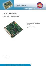
CXB-6S User‘s <strong>Manual</strong><br />
<strong>MSC</strong> CXB-6S / CXB-6SI<br />
COM Express Module<br />
Type 2 Pin-out<br />
based on<br />
2 nd / 3 rd Generation Intel ® Core Processor Family<br />
with<br />
Intel ® 6 / 7 Series Chipset<br />
Rev. 1.1<br />
2013-01-22
<strong>MSC</strong> CXB-6S / CXB-6SI <strong>User's</strong> <strong>Manual</strong><br />
Preface<br />
Copyright Notice<br />
Copyright © 2008 <strong>MSC</strong> <strong>Vertriebs</strong> <strong>GmbH</strong>. All rights reserved.<br />
Copying of this document, and giving it to others and the use or communication of the contents<br />
thereof, is forbidden without express authority. Offenders are liable to the payment of damages.<br />
All rights are reserved in the event of the grant of a patent or the registration of a utility model or<br />
design.<br />
Important Information<br />
This documentation is intended for qualified audience only. The product described herein is not<br />
an end user product. It was developed and manufactured for further processing by trained<br />
personnel.<br />
Disclaimer<br />
Although this document has been generated with the utmost care no warranty or liability for<br />
correctness or suitability for any particular purpose is implied. The information in this document<br />
is provided “as is” and is subject to change without notice.<br />
EMC Rules<br />
This unit has to be installed in a shielded housing. If not installed in a properly shielded<br />
enclosure, and used in accordance with the instruction manual, this product may cause radio<br />
interference in which case the user may be required to take adequate measures at his or her<br />
owns expense.<br />
Trademarks<br />
All used product names, logos or trademarks are property of their respective owners.<br />
Certification<br />
<strong>MSC</strong> <strong>Vertriebs</strong> <strong>GmbH</strong> is certified according to DIN EN ISO 9001:2000 standards.<br />
Life-Cycle-Management<br />
<strong>MSC</strong> products are developed and manufactured according to high quality standards. Our lifecycle-management<br />
assures long term availability through permanent product maintenance.<br />
Technically necessary changes and improvements are introduced if applicable. A product-<br />
change-notification and end-of-life management process assures early information of our<br />
customers.<br />
Product Support<br />
<strong>MSC</strong> engineers and technicians are committed to provide support to our customers whenever<br />
needed.<br />
Before contacting Technical Support of <strong>MSC</strong> <strong>Vertriebs</strong> <strong>GmbH</strong>, please consult the respective<br />
pages on our web site at www.mscembedded.com for the latest documentation, drivers and<br />
software downloads.<br />
If the information provided there does not solve your problem, please contact our Technical<br />
Support:<br />
Email: support.boards@mscembedded.com<br />
Phone: +49 8165 906-200<br />
2
<strong>MSC</strong> CXB-6S / CXB-6SI <strong>User's</strong> <strong>Manual</strong><br />
Content<br />
1 General Information............................................................................................................................... 5<br />
1.1 Revision History ............................................................................................................................. 5<br />
1.2 Reference Documents ................................................................................................................... 5<br />
1.3 Introduction .................................................................................................................................... 6<br />
2 Technical Description ............................................................................................................................ 7<br />
2.1 Key features ................................................................................................................................... 7<br />
2.2 Block diagram ................................................................................................................................ 8<br />
2.3 COM Express implementation ....................................................................................................... 9<br />
2.4 Functional units ............................................................................................................................ 10<br />
2.5 Power Supply ............................................................................................................................... 11<br />
2.6 Power Dissipation ........................................................................................................................ 11<br />
2.6.1 Running Mode....................................................................................................................... 11<br />
2.6.2 Power Dissipation (Standby Modes) .................................................................................... 12<br />
2.7 System Memory ........................................................................................................................... 13<br />
2.8 Mechanical Dimensions ............................................................................................................... 13<br />
2.8.1 Compact module ................................................................................................................... 13<br />
2.9 Thermal specifications ................................................................................................................. 14<br />
2.10 Signal description ..................................................................................................................... 15<br />
2.10.1 High Definition Audio ............................................................................................................ 15<br />
2.10.2 Ethernet ................................................................................................................................ 16<br />
2.10.3 IDE ........................................................................................................................................ 16<br />
2.10.4 Serial ATA ............................................................................................................................. 17<br />
2.10.5 PCI Express Lanes ............................................................................................................... 18<br />
2.10.6 PCI Express x16Graphic Lanes............................................................................................ 18<br />
2.10.7 Express Card Support .......................................................................................................... 19<br />
2.10.8 PCI Bus ................................................................................................................................. 19<br />
2.10.9 USB ....................................................................................................................................... 20<br />
2.10.10 LPC Bus ................................................................................................................................ 21<br />
2.10.11 LVDS Flat Panel ................................................................................................................... 21<br />
2.10.12 Analog VGA .......................................................................................................................... 21<br />
2.10.13 Digital Display Interfaces ...................................................................................................... 22<br />
2.10.14 Miscellaneous ....................................................................................................................... 25<br />
2.10.15 Power and System Management.......................................................................................... 26<br />
2.10.16 General Purpose I/O ............................................................................................................. 27<br />
2.10.17 SPI Interface ......................................................................................................................... 28<br />
2.10.18 Module Type Definition ......................................................................................................... 29<br />
2.10.19 Power and GND .................................................................................................................... 30<br />
2.11 Pin List for <strong>MSC</strong> CXB-6S module (Type 2) .............................................................................. 31<br />
2.12 DDI port pin assignment ........................................................................................................... 33<br />
3 Jumpers and Connectors .................................................................................................................... 35<br />
3.1 Jumpers ....................................................................................................................................... 35<br />
3.2 Fan Connector ............................................................................................................................. 36<br />
4 Watchdog ............................................................................................................................................ 36<br />
5 System resources ................................................................................................................................ 37<br />
5.1 PCI IRQ Routing .......................................................................................................................... 37<br />
5.2 IRQ Lines in APIC Mode .............................................................................................................. 38<br />
5.3 Carrier Board PCI Resource Allocation ....................................................................................... 39<br />
5.4 SMB Address Map ....................................................................................................................... 39<br />
6 BIOS .................................................................................................................................................... 40<br />
6.1.6 The Main Menu ..................................................................................................................... 43<br />
6.1.7 The Advanced Menu ............................................................................................................. 45<br />
3
<strong>MSC</strong> CXB-6S / CXB-6SI <strong>User's</strong> <strong>Manual</strong><br />
6.1.9 Chipset .................................................................................................................................. 60<br />
6.1.12 Boot ....................................................................................................................................... 70<br />
6.1.13 Security ................................................................................................................................. 71<br />
6.1.14 The Save & Exit Menu .......................................................................................................... 72<br />
6.2 BIOS and Firmware Update ......................................................................................................... 73<br />
6.7 Tech Notes ................................................................................................................................... 76<br />
7 Troubleshooting ................................................................................................................................... 80<br />
4
<strong>MSC</strong> CXB-6S / CXB-6SI <strong>User's</strong> <strong>Manual</strong><br />
1 General Information<br />
1.1 Revision History<br />
Rev. Date Description<br />
1.0 29.10.2012 Final formatting; released version<br />
1.1 22.01.2013 Minor changes<br />
1.2 Reference Documents<br />
[1] COM Express Module Base Specification<br />
COM Express Revision 2.0<br />
Last update: August 8 th , 2010<br />
[2] PCI Local Bus Specification Rev. 2.1<br />
PCI21.PDF<br />
Last update: June 1 st , 1995<br />
http://www.pcisig.com<br />
[3] ATA/ATAPI-6 Specification<br />
d1410r3b.pdf<br />
http://www.t13.org/<br />
[4] Serial ATA Specification<br />
Serial ATA 1.0 gold.pdf<br />
Last update: August 29 th , 2002 Rev.1.0<br />
http://www.sata-io.org/<br />
[5] IEEE Std. 802.3-2002<br />
802.3-2002.pdf<br />
http://www.ieee.org<br />
[6] Universal Bus Specification<br />
usb_20.pdf<br />
Last update: April 27 th , 2000<br />
http://www.usb.org<br />
[7] 2 nd Generation Intel® Core Processor Family Mobile and Intel Celeron® Processor Family<br />
Mobile Datasheet, Volume 1<br />
2nd-gen-core-family-mobile-vol-1-datasheet.pdf<br />
Last update: September 2011<br />
http://www.intel.com/content/www/us/en/processors/core/CoreTechnicalResources.html<br />
[8] 2 nd Generation Intel® Core Processor Family Mobile and Intel Celeron® Processor Family<br />
Mobile Datasheet, Volume 2<br />
2nd-gen-core-family-mobile-vol-2-datasheet.pdf<br />
Last update: June 2011<br />
http://www.intel.com/content/www/us/en/processors/core/CoreTechnicalResources.html<br />
[9] Mobile 3rd Generation Intel® Core Processor Family Datasheet – Volume 1 of 2<br />
3rd-gen-core-family-mobile-vol-1-datasheet.pdf<br />
Last update: September 2012<br />
http://www.intel.com/content/www/us/en/processors/core/CoreTechnicalResources.html<br />
[10] Mobile 3rd Generation Intel® Core Processor Family Datasheet – Volume 2 of 2<br />
3rd-gen-core-family-mobile-vol-2-datasheet.pdf<br />
Last update: June 2012<br />
http://www.intel.com/content/www/us/en/processors/core/CoreTechnicalResources.html<br />
[11] Intel® 6 Series Chipset and Intel® C200 series Chipset Datasheet<br />
6-chipset-c200-chipset-datasheet.pdf<br />
Last update: May 2011<br />
http://www.intel.com/products/notebook/chipsets/6series/technicaldocuments.htm<br />
[12] Intel® 6 Series Chipset and Intel® C200 series Chipset Specification Update<br />
6-and-c200-chipset-specification-update.pdf<br />
Last update: August 2011<br />
http://www.intel.com/products/notebook/chipsets/6series/technicaldocuments.htm<br />
5
<strong>MSC</strong> CXB-6S / CXB-6SI <strong>User's</strong> <strong>Manual</strong><br />
[13] Intel ® 7Series / C216 Chipset Family Platform Controller Hub (PCH) Datasheet<br />
7-series-chipset-pch-datasheet.pdf<br />
Last update: June 2012<br />
http://www.intel.com/content/www/us/en/chipsets/7-series-chipset-pchdatasheet.html?wapkw=intel+7+series+chipsets<br />
[14] Intel ® 7Series / C216 Chipset Family Platform Controller Hub (PCH) Family Specification Update<br />
7-series-chipset-pch-spec-update.pdf<br />
Last update: August 2012 Revision 010<br />
http://www.intel.com/content/www/us/en/chipsets/7-series-chipset-pch-specupdate.html?wapkw=intel+7+series+chipsets<br />
1.3 Introduction<br />
COM Express, an open specification of the PICMG (PCI Industrial Computer Manufacturer Group), is a<br />
module concept to bring PCI Express and other latest technologies like SATA, USB 2.0 and LVDS on a<br />
COM (Computer On Module).<br />
A COM Express module is plugged onto an application-specific base board similar to the ETX concept,<br />
but offers more options and a growth path to future CPU technologies. Utilizing different sizes, COM<br />
Express can be used for highly embedded solutions up to high performance platforms.<br />
The design of the <strong>MSC</strong> CXB-6S module supports the 2 nd Generation Intel® Core Processor Family<br />
enabling you to boost your embedded application to highest performance levels.<br />
For evaluation and design-in of the COM Express modules we offer evaluation baseboards and<br />
develop motherboards providing the interface infrastructure for the COM Express module using PC<br />
type connectors for external access.<br />
Currently three module sizes are defined in the COM Express Specification 2.0: the Compact Module,<br />
Basic Module and the Extended Module. The primary difference between them is the over-all physical<br />
size and the performance envelope supported by each. The Extended Module is the largest and can<br />
support larger processor and memory solutions. The Basic Module is the most common supporting typical<br />
processor platforms in the embedded world. The Compact Module is the smallest one and is intended to<br />
be used when designing with processors and chipsets in small form factor footprints (SFF).<br />
All module sizes use the same connectors and pin-outs and utilize several common mounting hole<br />
positions. This level of compatibility allows that a carrier board designed to accommodate an Extended<br />
Module can also support a Basic or Compact Module.<br />
Up to 440 pins of connectivity are available between COM Express modules and the Carrier Board.<br />
Legacy buses such as PCI, parallel ATA, LPC, HDA are supported as well as new high speed serial<br />
interconnects such as PCI Express, Serial ATA and Gigabit Ethernet.<br />
To enhance interoperability between COM Express modules and Carrier Boards, seven common<br />
signaling configurations (Pin-out Types) have been defined to ease system integration.<br />
6
<strong>MSC</strong> CXB-6S / CXB-6SI <strong>User's</strong> <strong>Manual</strong><br />
2 Technical Description<br />
2.1 Key features<br />
The <strong>MSC</strong> CXB-6S COM Express module is designed as a type 2 module according to COM Express®<br />
Module Base Specification Revision 2.0 and is also drop in compatible with carrier boards designed<br />
according to COM Express® Base Specification R1.0.<br />
Key features include:<br />
Module size: 125 mm x 95 mm<br />
Various 2 nd and 3 rd Generation Intel® Core Processors<br />
Dual 220 pin connector (440 pins)<br />
2x DDR3 SO-DIMM module up to 8 GB each one<br />
Eight USB 2.0 ports; 4 shared over-current lines<br />
Four Serial ATA ports with data rates up to 3.0Gb/s (300MB/s)<br />
Optional SATA NAND Flash Silicon Disk (4 GB to 32 GB)<br />
Five PCI Express x1 lanes<br />
Support pins for two ExpressCards<br />
Dual 24-bit LVDS channel<br />
Analog VGA<br />
High definition digital audio interface (external CODEC)<br />
Single Gbit Ethernet interface<br />
LPC interface<br />
Support for following Super IO : Winbond 83627<br />
Four GPI pins<br />
Four GPO pins<br />
+12V primary power supply input<br />
+5V standby (optional) and 3.3V RTC power supply inputs<br />
32 bit PCI interface<br />
IDE port (to support legacy ATA devices such as CD-ROM drives and Compact Flash storage<br />
cards)<br />
21 PCI Express lanes (5 on A-B and 16 on C-D)<br />
16 of 21 PCI Express lanes used for PCI Express Graphics<br />
Up to three digital display interfaces configurable as SDVO, HDMI, DVI or DisplayPort (pins<br />
shared with PCI Express Graphics)<br />
TPM module (option, TPM 1.2, SLB9635)<br />
Automatic fan control<br />
Watchdog timer<br />
Embedded Application Programming Interface (EAPI)<br />
7
2.2 Block diagram<br />
COM Express Connector A/B<br />
VCCRTC<br />
+5VSBY<br />
+12V<br />
GND<br />
GBE0_MDI<br />
2k<br />
EeeP<br />
<strong>MSC</strong> CXB-6S / CXB-6SI <strong>User's</strong> <strong>Manual</strong><br />
CMOS<br />
Backup<br />
16Mb<br />
SPI<br />
Flash<br />
82579<br />
GbE<br />
PHY<br />
WDT<br />
CPU FAN<br />
Connector<br />
SMBus<br />
5x PCIe x1<br />
SATA<br />
SSD<br />
DDR3 SODIMM<br />
Socket<br />
HW-<br />
Monitor<br />
PCIe x1<br />
PECI<br />
PWR-Ctrl, SLP-States, Thermals, Misc.<br />
8x USB 2.0<br />
2Ch. / 24Bit - LVDS<br />
VGA<br />
HD Audio<br />
4x GPI, 4x GPO<br />
2x SATA-6G<br />
2x SATA-3G<br />
16Mb<br />
SPI<br />
Flash<br />
I²C<br />
LPC Bus<br />
SPI Bus<br />
TPM<br />
1x PCIe x1<br />
1x SATA-3G<br />
64bit/1600MT/s 64bit/1600MT/s<br />
Sandy Bridge-Mbl<br />
PCIe[7]<br />
USB[0:5, 7:9]<br />
LVDS_A/B<br />
VGA<br />
HDA<br />
GPIOs<br />
SATA[0:1]<br />
SATA[2:3]<br />
GPIOs<br />
SATA[4]<br />
SPI<br />
LPC<br />
CPU<br />
8<br />
FDI<br />
PCH<br />
GPIOs<br />
Watch<br />
-Dog<br />
DMI<br />
DDP_B<br />
DDP_C<br />
DDP_D<br />
PCIe[6]<br />
PCIe[5]<br />
PCIe[0:4]<br />
DDR3 SODIMM<br />
Socket<br />
CPU Debug<br />
PCIe x16<br />
SDVO / HDMI /DVI/ DP<br />
HDMI / DVI / DP/eDP<br />
PCH Debug<br />
PCIe x1<br />
+<br />
HDMI / DVI / DP<br />
PCIe x1<br />
+<br />
PCH Debug<br />
optionally<br />
XDP-60<br />
A<br />
B<br />
PCIe-MUX<br />
SEL A#/B<br />
JMB368<br />
PCIe2PATA<br />
Master/Slave<br />
TI<br />
XIO2001<br />
PCIe2PCI<br />
Bridge<br />
TYPE[2:0]#<br />
+12V<br />
GND<br />
IDE<br />
32-bit PCI Bus<br />
Type 2<br />
COM Express R2.0 Module<br />
<strong>MSC</strong> CXB-6S/6SI<br />
PEG<br />
PEG_ENABLE#<br />
Rev. 08<br />
COM Express Connector C/D
<strong>MSC</strong> CXB-6S / CXB-6SI <strong>User's</strong> <strong>Manual</strong><br />
2.3 COM Express implementation<br />
COM Express required and optional features of pin-out type 2 are summarized in the following table.<br />
The features identified as Minimum (Min.) shall be implemented by all modules. Features identified up to<br />
Maximum (Max) may be additionally implemented by a module.<br />
The column <strong>MSC</strong> CXB-6S shows the implemented features of the <strong>MSC</strong> module.<br />
System I/O<br />
Type 2 <strong>MSC</strong> CXB-6S Note<br />
Min / Max<br />
PCI Express Graphics (PEG) 0 / 1 1 signals are multiplexed with SDVO signals<br />
PCI Express Lanes 0 - 5 1 / 6 5 (x1) 6 (x1) as an option if no PCI bus is needed<br />
PCI Express Lanes 16-31<br />
(same as PEG pins)<br />
0 / 16 1 (x16) off-module x16 PCI Express Graphics<br />
SDVO Channels 0 / 2 1 signals are multiplexed with PEG signals<br />
HDMI/DVI 0 /0 3 signals are multiplexed with PEG signals<br />
DisplayPort 1.1a 0 / 0 3 signals are multiplexed with PEG signals<br />
LVDS Channels 0 / 2 2 1x dual channel, 2x24 Bit<br />
VGA Port 0 / 1 1<br />
TV-Out NA 0 not available<br />
PATA Port 1 / 1 1 JMicron PCIe-PATA Controller JMB368<br />
SATA Ports 1 / 4 4/(1 x SSD)<br />
4x 300MB/s (ports 0 -3)<br />
optional 1 x Solid State Disk (port 4)<br />
HDA Digital Interface 0 / 1 1<br />
USB 2.0 Ports 4 / 8 8<br />
USB Client 0 / 1 0<br />
Gbit LAN 1 / 1 1 Intel 82597LM GbE PHY<br />
PCI Bus - 32 Bit 1 / 1 1<br />
Texas Instruments PCIe-to-PCI Bridge<br />
XIO2001<br />
Express Card Support 1 / 2 2<br />
LPC Bus 1 / 1 1<br />
SPI 1 / 2 2<br />
System Management<br />
General Purpose Inputs 4 / 4 4<br />
General Purpose Outputs 4 / 4 4<br />
SMBus 1 / 1 1<br />
I 2 C 1 / 1 1<br />
Watch Dog Timer 0 / 1 1<br />
Speaker Out 1 / 1 1<br />
External BIOS ROM support 0 / 2 2<br />
Reset Functions 1 / 1 1<br />
Power Management<br />
Thermal Protection 0 / 1 1<br />
Battery Low Alarm 0 / 1 1<br />
Suspend 0 / 1 1<br />
Wake 0 / 2 2<br />
Power Button Support 1 / 1 1<br />
Power Good 1 / 1 1<br />
TPM 0 / 0 1 optional TPM 1.2 module<br />
9
<strong>MSC</strong> CXB-6S / CXB-6SI <strong>User's</strong> <strong>Manual</strong><br />
2.4 Functional units<br />
CPUs<br />
(FCBGA-1023)<br />
Intel® Core i7-3615QE (Quad Core, 2.3GHz, 6MB, SV 45W.)<br />
Intel® Core i7-3612QE (Quad Core, 2.1GHz, 6MB, SV 35W.)<br />
Intel® Core i7-3555LE (Dual Core, 2.5GHz, 4MB, LV 25W.)<br />
Intel® Core i7-3517UE (Dual Core, 2.1GHz, 4MB, ULV 17W.)<br />
Intel® Core i5-3610ME (Dual Core, 2.7GHz, 3MB, SV 35W.)<br />
Intel® Core i3-3120ME (Dual Core, 2.4GHz, 3MB, SV 35W.)<br />
Intel® Core i3-3217UE (Dual Core, 1.6GHz, 3MB, ULV 17W.)<br />
Intel® Core i7-2715QE (Quad Core, 2.1GHz, 6MB, SV 45W.)<br />
Intel® Core i7-2655LE (Dual Core, 2.1GHz, 4MB, LV 25W).<br />
Intel® Core i7-2610UE (Dual Core, 1.5GHz, 3MB, ULV 17W).<br />
Intel® Core i5-2515E (Dual Core, 2.1GHz, SV 35W).<br />
Intel® Core i3-2310E (Dual Core, 2.1GHz, SV 35W).<br />
Intel® Celeron® B810E (Dual Core, 1.6GHz, SV 35W).<br />
Intel® Celeron® 847E (Dual Core, 1.1GHz, 2MB, ULV 17W).<br />
Intel® Celeron® 827E (Single Core, 1.4GHz, 1.5MB, ULV 17W).<br />
Intel® Celeron® 807UE (Single Core, 1.0GHz, 1MB, ULV 10W).<br />
Chipset Intel® 82QM77 with Intel® Core i5-3 and Intel® Core i7-3 processor SKUs.<br />
Intel® 82QM76 with Intel® Core i3-3 processor SKUs.<br />
Intel® 82QM67 with Intel® Core i5-2 and Intel® Core i7-2 processor SKUs.<br />
Intel® 82HM65 with Intel® Core i3-2 and Intel® Celeron® processor SKUs.<br />
Memory Two 204-pin DDR3 SO-DIMM sockets for up to 16GB (4GB with Intel® Celeron®<br />
807UE) non-ECC unbuffered DDR3 (One socket for up to 4GB on COM Express<br />
modules with Intel® Celeron® 807UE). Max. height 1250mil = 31.75mm.<br />
PC3-8500/ 10600 DDR3 SDRAM (DDR3-1066/1333).<br />
PC3-12800 DDR3 SDRAM (DDR3-1600) with Core i7-2715QE and Core i3/5/7-3.<br />
SATA 4 SATA channels up to 300MB/s each.<br />
EIDE 1 Enhanced IDE port ATA/UDMA100.<br />
USB 8 x USB 2.0.<br />
COM Express Type 2 interface, fully compliant to COM Express Base Specification R2.0.<br />
PCI Express Five channels PCIe x1.<br />
PCI 32 Bit standard interface.<br />
LPC Low Pin Count Bus for heritage interfaces.<br />
SPI Serial Peripheral Interface for up to two SPI flash devices.<br />
Graphics Controller Intel HD Graphics 2000/3000/4000 depending on processor SKU.<br />
Video Memory Intel® Dynamic Video Memory Technology (Intel® DVMT 5.0)<br />
LVDS Dual channel 24-bit LVDS (1.600 x 1.200 @ 60 Hz).<br />
Digital Display Ports DDPort B configurable as<br />
(multiplexed with HDMI/DVI (1920 x 1200 @ 60 Hz), DP (2560 x 1600 @ 60 Hz) and SDVO (200<br />
PEG) MP/s).<br />
DDPort C configurable as<br />
HDMI/DVI (1920 x 1200 @ 60 Hz) and DP (2560 x 1600 @ 60 Hz).<br />
DDPort D configurable as<br />
HDMI/DVI (1920 x 1200 @ 60 Hz), DP (2560 x 1600 @ 60 Hz) and eDP .<br />
PEG PCIe x16 graphics port (PEG) supports external graphics cards<br />
(not available on Intel® Celeron® 807UE processor).<br />
CRT Interface 340.4 MHz RAMDAC (2.048 x 1.536 @ 75 Hz).<br />
Ethernet 10/100/1000Base-TX (Intel® 82579LM).<br />
Sound Interface Intel® High Definition Audio Interface.<br />
Support for up to three external Codecs.<br />
Integrated DisplayPort/HDMI Audio support.<br />
Watchdog Timer PIC12C509A, creates system reset (programmable timeout, 1s … 255h).<br />
TPM (option) Optional TPM module, TPM 1.2, SLB9635.<br />
Fan Supply 4-pin header for support of a 12V PWM fan.<br />
Real Time Clock RTC integrated in PCH.<br />
CMOS Battery External.<br />
10
<strong>MSC</strong> CXB-6S / CXB-6SI <strong>User's</strong> <strong>Manual</strong><br />
System Monitoring Voltages, temperatures, fan<br />
Core voltage<br />
3.3V onboard voltage<br />
12V input voltage<br />
5V SBY input voltage<br />
CPU temperature (0°C - 100°C)<br />
System memory temperature<br />
Board temperature<br />
Fan speed and automatic fan speed control<br />
2.5 Power Supply<br />
+12V primary power supply input<br />
+5V standby<br />
Option, is not required for module operation.<br />
If not present, customer has to make sure that the supply voltages which are generated on the carrier<br />
board are switched off during suspend states, so that no current from the carrier board’s signal lines<br />
can flow to the CPU board.<br />
3.3V RTC power supply<br />
Option, is not required for module operation.<br />
BIOS SETUP data is stored in a non volatile backup memory device, therefore configuration data will<br />
not get lost during power off (except for time and date information)<br />
Voltage Input range Power Consumption<br />
+12V +11.4V - 12.6 V<br />
+5V Standby +4.75V - 5.25 V<br />
11<br />
Refer to chapter 2.6<br />
+3V RTC power supply +2.0V - 3.3V Typ. 1.8 µA<br />
2.6 Power Dissipation<br />
2.6.1 Running Mode<br />
All measurements were made by plugging the module onto a <strong>MSC</strong> CX-EVA2 evaluation board. The<br />
module was equipped with two 4GByte memory modules NANYA NT4GC64B8HB0NS-CG 1112.CN,<br />
4GB 2Rx8 PC3-10600S-9-10-F2.1333. The table below shows typical values which refer to<br />
consumption of the module itself without consumption of the base board and CPU fan.<br />
The following applications have been tested at room temperature.<br />
1. DOS prompt.<br />
2. Windows desktop (idle) under Microsoft Windows 7 Professional 64-bit SP1.<br />
3. Running Intel® Thermal Analysis Tool (TAT!) Ver. 4.3 to achieve 70% CPU workload on each<br />
processor core/thread and 100% Graphics workload as recommended by Intel under Microsoft<br />
Windows 7 Professional 64-bit SP1.<br />
<strong>MSC</strong> CXB-6S-010<br />
Intel® Celeron® 807UE (10W)<br />
<strong>MSC</strong> CXB-6S-009<br />
Intel® Celeron® 827E (17W)<br />
<strong>MSC</strong> CXB-6S-008<br />
Intel® Core i7-2715QE (45W)<br />
<strong>MSC</strong> CXB-6S-007<br />
Intel® Core i7-2655LE (25W)<br />
<strong>MSC</strong> CXB-6S-006<br />
Intel® Core i7-2610UE (17W)<br />
<strong>MSC</strong> CXB-6S-005<br />
Intel® Core i5-2515E (35W)<br />
<strong>MSC</strong> CXB-6S-004<br />
Intel® Core i3-2310E (35W)<br />
Module / CPU DOS Win 7 Idle<br />
Win 7 TAT!<br />
long term max. 1)<br />
11.5W 8 W 19 W - 2)<br />
13 W 8.5 W 25 W - 2)<br />
19 W 9.5 W 64 W 75 W<br />
17 W 8.5 W 41 W 47 W<br />
18 W 8.5 W 30 W 36 W<br />
20 W 9 W 52 W 61 W<br />
19 W 8.5 W 47 W - 2)
<strong>MSC</strong> CXB-6S / CXB-6SI <strong>User's</strong> <strong>Manual</strong><br />
<strong>MSC</strong> CXB-6S-002<br />
Intel® Celeron® 847E (17W)<br />
12 W 8.5 W 28 W - 2)<br />
<strong>MSC</strong> CXB-6S-001<br />
Intel® Celeron® B810E (35W)<br />
18 W 9 W 40 W - 2)<br />
<strong>MSC</strong> CXB-6SI-011<br />
Intel® Core i7-3612QE (35W)<br />
14 W 9 W 53 W 75 W<br />
<strong>MSC</strong> CXB-6SI-008<br />
Intel® Core i7-3615QE (45W)<br />
14 W 12.5 W 65 W 76 W<br />
<strong>MSC</strong> CXB-6SI-005<br />
Intel® Core i5-3610ME (35W)<br />
15 W 9 W 51 W 58 W<br />
1) Due to the Intel® Turbo Boost Technology 2.0 feature on 2 nd Generation Intel® Core i5 and<br />
2 nd Generation Intel® Core i7 processors the maximum power consumption for short durations<br />
may be higher than the long term power consumption. The power supply must be able to deliver<br />
this additional amount of power.<br />
2) The Intel® Turbo Boost Technology 2.0 feature is not available on 2 nd Generation Intel® Core i3<br />
and Intel® Celeron® processors.<br />
2.6.2 Power Dissipation (Standby Modes)<br />
1. System is shut down into “Soft Off” (S5) or “Suspend to Disk” (S4) by Windows 7 Professional 64-bit<br />
SP1.<br />
2. System is shut down into “Soft Off” (S5) or “Suspend to Disk” (S4) by Windows 7 Professional 64bit<br />
SP1 with Wake On LAN enabled.<br />
3. System is shut down into “Suspend to RAM” (S3) by Windows 7 Professional 64-bit SP1.<br />
4. System is shut down into “Suspend to RAM” (S3) by Windows 7 Professional 64-bit SP1 with Wake<br />
On LAN enabled.<br />
Module / CPU<br />
<strong>MSC</strong> CXB-6S-009<br />
Intel® Celeron 827E (17W)<br />
<strong>MSC</strong> CXB-6S-004<br />
Intel® Core i3-2310E (35W)<br />
<strong>MSC</strong> CXB-6S-001<br />
Intel® Celeron B810E (35W)<br />
<strong>MSC</strong> CXB-6S-010<br />
Intel® Celeron 807UE (10W)<br />
<strong>MSC</strong> CXB-6S-008<br />
Intel® Core i7-2715QE (45W)<br />
<strong>MSC</strong> CXB-6S-006<br />
Intel® Core i7-2610UE (17W)<br />
<strong>MSC</strong> CXB-6S-005<br />
Intel® Core i5-2515E (35W)<br />
<strong>MSC</strong> CXB-6S-002<br />
Intel® Celeron 847E (17W)<br />
<strong>MSC</strong> CXB-6S-007<br />
Intel® Core i7-2655LE (25W)<br />
<strong>MSC</strong> CXB-6SI-011<br />
Intel® Core i7-3612QE (35W)<br />
<strong>MSC</strong> CXB-6SI-008<br />
Intel® Core i7-3615QE (45W)<br />
<strong>MSC</strong> CXB-6SI-005<br />
Intel® Core i5-3610ME (35W)<br />
Input<br />
Power<br />
12<br />
no<br />
WOL<br />
S3 S4 / S5<br />
WOL<br />
enabled<br />
no<br />
WOL<br />
WOL<br />
enabled<br />
12V/5V_SBY 0.6 W 0.7 W 0.4 W 0.5 W<br />
12V only 0.7 W 0.8 W 0.5 W 0.6 W<br />
12V/5V_SBY 0.9 W 1.0 W 0.4 W 0.5 W<br />
12V only 1.3 W 1.4 W 0.5 W 0.6 W<br />
12V/5V_SBY 0.9 W 1.0 W 0.5 W 0.5 W<br />
12V only 1.4 W 1.5 W 0.7 W 0.8 W
<strong>MSC</strong> CXB-6S / CXB-6SI <strong>User's</strong> <strong>Manual</strong><br />
2.7 System Memory<br />
The <strong>MSC</strong> CXB-6S CPU module provides two sockets (only one socket on CXB-6S-010) for memory<br />
modules which have to meet the following demands:<br />
204pin unbuffered non-ECC DDR3 SO-DIMM, Raw Card A, B, C and F.<br />
1.5V Supply Voltage<br />
DDR3-1066 / PC3-8500, DDR3-1333 / PC3-10600<br />
DDR3-1600 / PC3-12800 with Core i7-2715QE and Core i3/5/7-3.<br />
Maximum module height: 30mm.<br />
SPD (Serial Presence Detect) EEPROM.<br />
2.8 Mechanical Dimensions<br />
2.8.1 Compact module<br />
There are two height options defined in the COM Express specification : 5mm and 8mm.<br />
The height option is defined by the connectors on the baseboard.<br />
13
<strong>MSC</strong> CXB-6S / CXB-6SI <strong>User's</strong> <strong>Manual</strong><br />
2.9 Thermal specifications<br />
The cooling solution of a COM Express module is based on a heat-spreader concept.<br />
A heat-spreader is a metal plate (typically aluminium) mounted on the top of the module. The connection<br />
between this plate and the module components is typically done by thermal interface materials like phase<br />
change foils, gap pads and copper or aluminium blocks. A very good thermal conductivity is required in<br />
order to conduct the heat from the CPU and the chipset to the heat-spreader plate.<br />
The heat-spreader of the <strong>MSC</strong> module is thermally attached using phase change materials and small<br />
aluminium blocks filling the gap between cpu and chipset dies and the heat-spreader plate.<br />
The heat-spreader is not a heat-sink! It is a defined thermal interface for the system designer with fixed<br />
mechanical dimensions, so it should be possible to change different module types without problems.<br />
There must be a cooling solution for the system. The surface temperature of the heat-spreader should not<br />
exceed 80°C.<br />
Main issue for the thermal functionality of a system is that each device of the module is operated within its<br />
specified thermal values. The max value for the CPU is 100°C and 108°C for the chipset. So there may<br />
be system implementations where the heat-spreader temperature could be higher.<br />
Anyway, in this case it has to be validated that there are no thermal specification violations of any<br />
assembled part or integrated circuit over the system temperature range even at worst case conditions.<br />
Additionally <strong>MSC</strong> offers adequate heat-sink solutions for the different CXB-6S modules depending on the<br />
power dissipation of the implemented CPU. For more information please refer to<br />
support.boards@mscembedded.com or contact your sales representative.<br />
14
2.10 Signal description<br />
<strong>MSC</strong> CXB-6S / CXB-6SI <strong>User's</strong> <strong>Manual</strong><br />
Pins are marked in the following tables with the power rail associated with the pin, and, for input and I/O pins, with the input voltage tolerance. The pin power rail and<br />
the pin input voltage tolerance may be different. For example, the PCI group is defined as having a 3.3V power rail, meaning that the output signals will only be<br />
driven to 3.3V, but the pins are tolerant of 5V signals.<br />
An additional label, “Sus”, indicates that the pin is active during suspend states (S3,S4,S5). If suspend modes are used, then care must be taken to avoid loading<br />
signals that are active during suspend to avoid excessive suspend mode current draw.<br />
I = Input.<br />
O = Output.<br />
OD = Open Drain output.<br />
I/OD = Bi-directional Input/Open Drain Output Pin.<br />
I/O = Bi-directional Input/Output.<br />
ePU = external pull-up resistor.<br />
ePD = external pull-down resistor.<br />
eSR = external series resistor (on COM Express module).<br />
iPU = integrated pull-up resistor, iPD = integrated pull-down resistor (inside PCH or other IC, real value may vary from nominal one).<br />
2.10.1 High Definition Audio<br />
Signal Pin Signal Power Remark / PU/PD/SR Description Source / Target<br />
Type Level Rail Tolerance<br />
HDA_RST# O CMOS 3.3V Sus eSR = 33 Ω Reset output to CODEC, active low. PCH<br />
HDA_SYNC O CMOS 3.3V Sus ePU =1 KΩ 48kHz fixed-rate, sample-synchronization signal to the CODEC(s), PCH<br />
iPD = 20 KΩ functional strap option sampled with rising edge of RSMRST#,<br />
eSR = 33 Ω iPD is disabled after RSMRST# de-assertion.<br />
HDA_BITCLK O CMOS 3.3V Sus eSR = 33 Ω 24.00 MHz serial data clock generated by the PCH PCH<br />
HDA_SDOUT O CMOS 3.3V Sus iPD = 20 KΩ Serial TDM data output to the CODEC, functional strap option, iPD is PCH<br />
eSR = 33 Ω disabled after PLTRST# de-assertion. Do not pull high externally.<br />
HDA_SDIN[0:2] I CMOS 3.3V Sus 3.3V iPD = 20 KΩ<br />
eSR = 33 Ω<br />
Serial TDM data inputs from up to 3 CODECs. PCH<br />
15
2.10.2 Ethernet<br />
<strong>MSC</strong> CXB-6S / CXB-6SI <strong>User's</strong> <strong>Manual</strong><br />
Signal Pin Signal Power Remark / PU/PD/SR Description Source / Target<br />
Type Level Rail Tolerance<br />
GBE0_MDI[0:3]+ I/O Analog 3.3V Sus 3.3V Gigabit Ethernet Controller 0: Media Dependent Interface Differential 82579LMi<br />
GBE0_MDI[0:3]-<br />
Pairs 0,1,2,3. The MDI can operate in 1000, 100 and 10 Mbit / sec<br />
modes.<br />
MDI[0]+/- B1_DA+/-<br />
MDI[1]+/- B1_DB+/-<br />
MDI[2]+/- B1_DC+/-<br />
MDI[3]+/- B1_DD+/-<br />
GBE0_ACT# OD CMOS 3.3V Sus 5V / 20 mA Gigabit Ethernet Controller 0 activity indicator, active low. 82579LM<br />
GBE0_LINK# OD CMOS 3.3V Sus 5V / 20 mA Gigabit Ethernet Controller 0 link indicator, active low. 82579LM<br />
GBE0_LINK100# OD CMOS 3.3V Sus 5V / 20 mA Gigabit Ethernet Controller 0 100 Mbit / sec link indicator, active low. 82579LM<br />
GBE0_LINK1000# OD CMOS 3.3V Sus 5V / 20 mA Gigabit Ethernet Controller 0 1000 Mbit / sec link indicator, active<br />
low.<br />
82579LM<br />
GBE0_CTREF REF N/A. Center tab voltage not needed by 82759LM.<br />
2.10.3 IDE<br />
Signal Pin Signal Power Remark / PU/PD/SR Description Source / Target<br />
Type Level Rail Tolerance<br />
IDE_D[0:6/8:15] I/O CMOS 3.3V 3.3V eSR = 33 Ω Bidirectional data to / from IDE device. JMB368<br />
IDE_D7 I/O CMOS 3.3V 3.3V eSR = 33 Ω<br />
iPD = 32 k Ω<br />
Bidirectional data to / from IDE device. JMB368<br />
IDE_A[0:2] O CMOS 3.3V 3.3V eSR = 33 Ω Address lines to IDE device. JMB368<br />
IDE_IOW# O CMOS 3.3V 3.3V eSR = 22 Ω I/O write line to IDE device. Data latched on trailing (rising) edge. JMB368<br />
IDE_IOR# O CMOS 3.3V 3.3V eSR = 22 Ω I/O read line to IDE device. JMB368<br />
IDE_REQ I CMOS 3.3V 3.3 V ePD = 5.6 KΩ IDE device DMA Request. Asserted by IDE device to request a data JMB368<br />
eSR = 82 Ω<br />
iPD = 32 KΩ<br />
transfer.<br />
IDE_ACK# O CMOS 3.3V 3.3V eSR 22Ω IDE Device DMA Acknowledge. JMB368<br />
IDE_CS1# O CMOS 3.3V 3.3V eSR = 33 Ω IDE Device Chip Select for 1F0h to 1FFh range. JMB368<br />
IDE_CS3# O CMOS 3.3V 3.3V eSR = 33 Ω IDE Device Chip Select for 3F0h to 3FFh range. JMB368<br />
IDE_IORDY I CMOS 3.3V 3.3 V ePU = 4.7 KΩ IDE device I/O ready input. Pulled low by the IDE device to extend JMB368<br />
eSR = 82 Ω<br />
iPU = 47 KΩ<br />
the cycle.<br />
IDE_RESET# O CMOS 3.3V 3.3V eSR = 33 Ω Reset output to IDE device, active low. JMB368<br />
IDE_IRQ I CMOS 3.3V 3.3 V ePD = 10 KΩ Interrupt request from IDE device. JMB368<br />
16
Signal Pin<br />
Type<br />
<strong>MSC</strong> CXB-6S / CXB-6SI <strong>User's</strong> <strong>Manual</strong><br />
Signal<br />
Level<br />
Power<br />
Rail<br />
Remark /<br />
Tolerance<br />
eSR = 82 Ω<br />
iPD = 32 KΩ<br />
IDE_CBLID# I CMOS 3.3V 3.3 V ePD = 100<br />
KΩ<br />
Note: The IDE interface is realized by a JMicron JMB368 PCIe-to-IDE controller located on PCIe lane #6.<br />
2.10.4 Serial ATA<br />
PU/PD/SR Description Source / Target<br />
Input from off-module hardware indicating the type of IDE cable<br />
being used. High indicates a 40-pin cable used for legacy IDE<br />
modes. Low indicates that an 80-pin cable with interleaved grounds<br />
is used. Such a cable is required for Ultra-DMA 66, 100 and 133<br />
modes.<br />
17<br />
JMB368<br />
Signal Pin Signal Power Remark / PU/PD/SR Description Source / Target<br />
Type Level Rail Tolerance<br />
SATA0_TX+ O SATA 3.3V AC coupled<br />
Serial ATA Channel 0 transmit differential pair. PCH<br />
SATA0_TX-<br />
on module<br />
SATA0_RX+ I SATA 3.3V AC coupled<br />
Serial ATA Channel 0 receive differential pair. PCH<br />
SATA0_RX-<br />
on module<br />
SATA1_TX+ O SATA 3.3V AC coupled<br />
Serial ATA Channel 1transmit differential pair. PCH<br />
SATA1_TX-<br />
on module<br />
SATA1_RX+ I SATA 3.3V AC coupled<br />
Serial ATA Channel 1 receive differential pair. PCH<br />
SATA1_RX-<br />
on module<br />
SATA2_TX+ O SATA 3.3V AC coupled<br />
Serial ATA Channel 2 transmit differential pair. PCH<br />
SATA2_TX-<br />
on module<br />
SATA2_RX+ I SATA 3.3V AC coupled<br />
Serial ATA Channel 2 receive differential pair. PCH<br />
SATA2_RX-<br />
on module<br />
SATA3_TX+ O SATA 3.3V AC coupled<br />
Serial ATA Channel 3 transmit differential pair. PCH<br />
SATA3_TX-<br />
on module<br />
SATA3_RX+ I SATA 3.3V AC coupled<br />
Serial ATA Channel 3 receive differential pair. PCH<br />
SATA3_RX-<br />
on module<br />
ATA_ACT# OD CMOS 3.3V 5V /20 mA SATA activity indicator, active low. PCH
2.10.5 PCI Express Lanes<br />
<strong>MSC</strong> CXB-6S / CXB-6SI <strong>User's</strong> <strong>Manual</strong><br />
Signal Pin Signal Power Remark / PU/PD/SR Description Source / Target<br />
Type Level Rail Tolerance<br />
PCIE_TX[0:4+ O PCIe 3.3V AC coupled<br />
PCI Express Differential Transmit Pairs 0 through 4 PCH<br />
PCIE_TX[0:4]-<br />
on module<br />
PCIE_RX[0:4]+ I PCIe 3.3V AC coupled<br />
PCI Express Differential Receive Pairs 0 through 4 PCH<br />
PCIE_RX[0:4]-<br />
off module<br />
PCIE_CLK_REF+ O PCIe 3.3V Differential Reference Clock output for all PCI Express and PCI PCH<br />
PCIE_CLK_REF- CLK<br />
Express Graphics lanes.<br />
Note: PCIe lanes #5 is used on the CXB-6S module and therefore not available for externally by default.<br />
2.10.6 PCI Express x16Graphic Lanes<br />
Signal Pin Signal Power Remark /<br />
Type Level Rail Tolerance<br />
PEG_TX[0:15]+ O PCIe 3.3V AC coupled<br />
PEG_TX[0:15]-<br />
on module<br />
PEG_RX[0:15]+<br />
PEG_RX[0:15]-<br />
I PCIe 3.3V AC coupled<br />
off module<br />
PU/PD/SR Description Source / Target<br />
PCI Express Graphics transmit differential pairs.<br />
These signals can also be used as standard PCI Express transmit<br />
lanes as PCIE_TX[16:31]+/- on type 4 and type 5 modules. Some of<br />
them are multiplexed with the digital display interface of the PCH<br />
(SDVO, DVI, HDMI or DisplayPort).<br />
PCI Express Graphics receive differential pairs.<br />
These signals can also be used as standard PCI Express receive<br />
lanes as PCIE_RX[16:31]+/- on type 5 and type 5 modules. Some of<br />
these signals are multiplexed with the digital display interface of the<br />
PCH (SDVO, DVI, HDMI or DisplayPort).<br />
PEG_RX5- I/O CMOS 3.3V 3.3V iPD = 20 KΩ DDPC_CTRLDATA, strap option, Port C detect,<br />
iPD is disabled after PLTRST# de-assertion.<br />
PEG_RX8- I/O CMOS 3.3V 3.3V iPD = 20 KΩ DDPD_CTRLDATA, strap option, Port D detect,<br />
iPD is disabled after PLTRST# de-assertion.<br />
PEG_LANE_RV# I CMOS 3.3V 3.3V ePU = 5.7 KΩ PCI Express Graphics lane reversal input strap.<br />
Pull low on the carrier board to reverse lane order. Be aware that the<br />
digital display interface that share this interface do not support<br />
reverse order functionality if this strap is low.<br />
PEG_ENABLE# I CMOS 3.3V 3.3V ePU = 10 KΩ PCI Express x16 external Graphics Enable Signal.<br />
Pull low to enable the x16 interface (PEG or PCIe).<br />
Pull high or leave as no connect to switch the PCHs digital display<br />
interface (port B, port C and port D) to the COM Express connector.<br />
Note: Module input signal PEG_ENABLE# (D97) must be low to select PEG/PCIe functionality.<br />
18<br />
CPU<br />
CPU<br />
CPU<br />
CPU<br />
CPU<br />
PCH / MUX
2.10.7 Express Card Support<br />
<strong>MSC</strong> CXB-6S / CXB-6SI <strong>User's</strong> <strong>Manual</strong><br />
Signal Pin Signal Power Remark / PU/PD Description Source / Target<br />
Type Level Rail Tolerance<br />
EXCD[0]_CPPE# I CMOS 3.3V 3.3V ePU = 10 KΩ ExpressCard card request, active low PCH<br />
EXCD[1]_CPPE# I CMOS 3.3V 3.3V ePU = 10 KΩ ExpressCard card request, active low PCH<br />
EXCD[0]_RST# O CMOS 3.3V 3.3V ePU = 8.2 KΩ ExpressCard reset, active low PCH<br />
EXCD[1]_RST# O CMOS 3.3V 3.3V ePU = 8.2 KΩ ExpressCard reset, active low PCH<br />
2.10.8 PCI Bus<br />
Signal Pin Signal Power Remark / PU/PD/SR Description Source / Target<br />
Type Level Rail Tolerance<br />
PCI_AD[0:31] I/O CMOS 3.3V 5V PCI bus multiplexed address and data lines XIO2001<br />
PCI_C/BE[0:3]# I/O CMOS 3.3V 5V PCI bus byte enable lines, active low XIO2001<br />
PCI_DEVSEL# I/O CMOS 3.3V 5V ePU = 8.2 KΩ PCI bus Device Select, active low. XIO2001<br />
PCI_FRAME# I/O CMOS 3.3V 5V ePU = 8.2 KΩ PCI bus Frame control line, active low. XIO2001<br />
PCI_IRDY# I/O CMOS 3.3V 5V ePU = 8.2 KΩ PCI bus Initiator Ready control line, active low. XIO2001<br />
PCI_TRDY# I/O CMOS 3.3V 5V ePU = 8.2 KΩ PCI bus Target Ready control line, active low. XIO2001<br />
PCI_STOP# I/O CMOS 3.3V 5V ePU = 8.2 KΩ PCI bus STOP control line, active low, driven by cycle initiator. XIO2001<br />
PCI_PAR I/O CMOS 3.3V 5V PCI bus parity XIO2001<br />
PCI_PERR# I/O CMOS 3.3V 5V ePU = 8.2 KΩ Parity Error: An external PCI device drives PERR# when it receives<br />
data that has a parity error.<br />
XIO2001<br />
PCI_REQ[0:3]# I CMOS 3.3V 5V ePU = 8.2 KΩ PCI bus master request input lines, active low. XIO2001<br />
PCI_GNT[0:3]# O CMOS 3.3V PCI bus master grant output lines, active low. XIO2001<br />
PCI_RESET# O CMOS 3.3V PCI Reset output, active low. XIO2001<br />
PCI_LOCK# I/O CMOS 3.3V 5V ePU = 8.2 KΩ PCI Lock control line, active low. XIO2001<br />
PCI_SERR# I/O CMOS 3.3V 5V ePU = 8.2 KΩ System Error: SERR# may be pulsed active by any PCI device that XIO2001<br />
OD<br />
detects a system error condition.<br />
PCI_PME# I CMOS 3.3V Sus 5V ePU = 8.2 KΩ PCI Power Management Event: PCI peripherals drive PME# to wake<br />
system from low-power states S1–S5.<br />
XIO2001<br />
PCI_CLKRUN# I/O CMOS 3.3V 5V ePU = 8.2 KΩ Bidirectional pin used to support PCI clock run protocol for mobile<br />
systems.<br />
XIO2001<br />
PCI_IRQ[A:D]# I CMOS 3.3V 5V ePU = 8.2 KΩ PCI interrupt request lines. XIO2001<br />
PCI_CLK O CMOS 3.3V eSR = 82 Ω PCI clock output.<br />
33 MHz if PCI_M66EN = low, 66 MHz if PCI_M66EN = high or open.<br />
XIO2001<br />
19
<strong>MSC</strong> CXB-6S / CXB-6SI <strong>User's</strong> <strong>Manual</strong><br />
Signal Pin Signal Power Remark / PU/PD/SR Description Source / Target<br />
Type Level Rail Tolerance<br />
PCI_M66EN I CMOS 3.3V 5V ePU = 10 KΩ Module input signal indicates whether an off-module PCI device is<br />
capable of 66MHz operation. Pulled to GND by Carrier Board device<br />
or by Slot Card if the devices are NOT capable of 66 MHz operation.<br />
XIO2001<br />
Note: The PCI bus is realized by a Texas Instruments XIO2001 PCIe-to-PCI bridge located on PCIe lane #5. Therefore PCIe lane #5 isn’t available for external use<br />
by default.<br />
2.10.9 USB<br />
Signal Pin Signal Power Remark / PU/PD/SR Description Source / Target<br />
Type Level Rail Tolerance<br />
USB[0:7]+<br />
USB[0:7]-<br />
I/O USB 3.3V Sus 3.3V USB differential pairs, channels 0 through 7 PCH<br />
USB_0_1_OC# I CMOS 3.3V Sus 3.3V ePU = 8.2 KΩ USB channels 0 and 1 over-current sense.<br />
A pull-up for this line is present on the module. An open drain driver<br />
from a USB current monitor on the Carrier Board may drive this line<br />
low.<br />
Do not pull this line high on the Carrier Board.<br />
PCH<br />
USB_2_3_OC# I CMOS 3.3V Sus 3.3V ePU = 8.2 KΩ USB channels 2 and 3 over-current sense.<br />
A pull-up for this line is present on the module. An open drain driver<br />
from a USB current monitor on the Carrier Board may drive this line<br />
low.<br />
Do not pull this line high on the Carrier Board.<br />
PCH<br />
USB_4_5_OC# I CMOS 3.3V Sus 3.3V ePU = 8.2 KΩ USB channels 4 and 5 over-current sense.<br />
A pull-up for this line is present on the module. An open drain driver<br />
from a USB current monitor on the Carrier Board may drive this line<br />
low.<br />
Do not pull this line high on the Carrier Board.<br />
PCH<br />
USB_6_7_OC# I CMOS 3.3V Sus 3.3V ePU = 8.2 KΩ USB channels 6 and 7 over-current sense.<br />
A pull-up for this line is present on the module. An open drain driver<br />
from a USB current monitor on the Carrier Board may drive this line<br />
low.<br />
Do not pull this line high on the Carrier Board.<br />
PCH<br />
20
2.10.10 LPC Bus<br />
<strong>MSC</strong> CXB-6S / CXB-6SI <strong>User's</strong> <strong>Manual</strong><br />
Signal Pin Signal Power Remark / PU/PD/SR Description Source / Target<br />
Type Level Rail Tolerance<br />
LPC_AD[0:3] I/O CMOS 3.3V 3.3V iPU = 20 KΩ LPC multiplexed address, command and data bus PCH<br />
LPC_FRAME# O CMOS 3.3V LPC frame indicates the start of an LPC cycle PCH<br />
LPC_DRQ[0:1]# I CMOS 3.3V 3.3V iPU = 20 KΩ LPC serial DMA request PCH<br />
LPC_SERIRQ I/OD CMOS 3.3V 3.3V ePU = 200 Ω LPC serial interrupt PCH<br />
LPC_CLK O CMOS 3.3V eSR = 22 Ω LPC clock output - 33MHz nominal PCH<br />
2.10.11 LVDS Flat Panel<br />
Signal Pin Signal Power Remark / PU/PD/SR Description Source / Target<br />
Type Level Rail Tolerance<br />
LVDS_A[0:3]+<br />
LVDS_A[0:3]-<br />
O LVDS LVDS Channel A differential pairs PCH<br />
LVDS_A_CK+<br />
LVDS_A_CK-<br />
O LVDS LVDS Channel A differential clock PCH<br />
LVDS_B[0:3]+<br />
LVDS_B[0:3]-<br />
O LVDS LVDS Channel B differential pairs PCH<br />
LVDS_B_CK+<br />
LVDS_B_CK-<br />
O LVDS LVDS Channel B differential clock PCH<br />
LVDS_VDD_EN O CMOS 3.3V ePD = 100 KΩ LVDS panel power enable PCH<br />
LVDS_BKLT_EN O CMOS 3.3V ePD = 100 KΩ LVDS panel backlight enable PCH<br />
LVDS_BKLT_CTRL O CMOS 3.3V LVDS panel backlight brightness control PCH<br />
LVDS_I2C_CK O CMOS 3.3V ePU = 2.2 KΩ I2C clock output for LVDS display use PCH<br />
LVDS_I2C_DAT I/OD CMOS 3.3V 3.3V ePU = 2.2 KΩ I2C data line for LVDS display use<br />
PCH<br />
iPD = 20 KΩ LVDS detect, iPD is disabled after PLTRST# de-assertion.<br />
2.10.12 Analog VGA<br />
Signal Pin Signal Power Remark / PU/PD/SR Description Source / Target<br />
Type Level Rail Tolerance<br />
VGA_RED O Analog ePD = 150 Ω Red for monitor. Analog DAC output, designed to drive a 37.5-Ohm<br />
equivalent load.<br />
PCH<br />
VGA_GRN O Analog ePD = 150 Ω Green for monitor. Analog DAC output, designed to drive a 37.5-<br />
Ohm equivalent load.<br />
PCH<br />
VGA_BLU O Analog ePD = 150 Ω Blue for monitor. Analog DAC output, designed to drive a 37.5-Ohm<br />
equivalent load.<br />
PCH<br />
21
<strong>MSC</strong> CXB-6S / CXB-6SI <strong>User's</strong> <strong>Manual</strong><br />
Signal Pin Signal Power Remark / PU/PD/SR Description Source / Target<br />
Type Level Rail Tolerance<br />
VGA_HSYNC O CMOS 3.3V Horizontal sync output to VGA monitor PCH<br />
VGA_VSYNC O CMOS 3.3V Vertical sync output to VGA monitor PCH<br />
VGA_I2C_CK O CMOS 3.3V ePU = 2.2 KΩ DDC clock line. I 2 C port dedicated to identify VGA monitor<br />
capabilities<br />
PCH<br />
VGA_I2C_DAT I/OD CMOS 3.3V 3.3V ePU = 2.2 KΩ DDC data line. I 2 C port dedicated to identify VGA monitor<br />
capabilities<br />
PCH<br />
2.10.13 Digital Display Interfaces<br />
The Intel Platform Controller Hub (PCH) provides three Digital Display Ports B, C and D that may be configured for SDVO, HDMI, DVI or DisplayPort functionality.<br />
These ports may be switched to the COM Express Connector C-D by a HIGH level on input signal PEG_ENABLE# (D97) instead of the CPUs PCI Express Graphic<br />
lanes. The pin-out is chosen in a way that the digital display ports are accessible through special ADD2-Cards that can be plugged into the PEG slot on existing<br />
COM Express type 2 carrier boards. Be aware that the digital display interface does not support reverse order functionality if PEG_LANE_RV# strap is low.<br />
2.10.13.1 SVDO (Digital Display Port B only)<br />
Signal Pin Signal Power Remark / PU/PD/SR Description Source / Target<br />
Type Level Rail Tolerance<br />
SDVOB_RED+ O PCIe AC coupled<br />
Serial Digital Video B red output differential pair<br />
PCH<br />
SDVOB_RED-<br />
on module<br />
Multiplexed with PEG_TX[0]+ and PEG_TX[0]-<br />
SDVOB_GRN+ O PCIe AC coupled<br />
Serial Digital Video B green output differential pair<br />
PCH<br />
SDVOB_GRN-<br />
on module<br />
Multiplexed with PEG_TX[1]+ and PEG_TX[1]-<br />
SDVOB_BLU+ O PCIe AC coupled<br />
Serial Digital Video B blue output differential pair<br />
PCH<br />
SDVOB_BLU-<br />
on module<br />
Multiplexed with PEG_TX[2]+ and PEG_TX[2]-<br />
SDVOB_CK+ O PCIe AC coupled<br />
Serial Digital Video B clock output differential pair.<br />
PCH<br />
SDVOB_CK-<br />
on module<br />
Multiplexed with PEG_TX[3]+ and PEG_TX[3]-<br />
SDVO_TVCLKIN+ I PCIe AC coupled<br />
Serial Digital Video B TVOUT Synchronization Clock input<br />
PCH<br />
SDVO_TVCLKIN-<br />
off module<br />
differential pair. Multiplexed with PEG_RX[0]+ and PEG_RX[0]-<br />
SDVO_INT+ I PCIe AC coupled<br />
Serial Digital Video Interrupt input differential pair.<br />
PCH<br />
SDVO_INT-<br />
off module<br />
Multiplexed with PEG_RX[1]+ and PEG_RX[1]-<br />
SDVO_FLDSTALL+ I PCIe AC coupled<br />
Serial Digital Video Field Stall input differential pair.<br />
PCH<br />
SDVO_FLDSTALL<br />
off module<br />
Multiplexed with PEG_RX[2]+ and PEG_RX[2]-<br />
SDVO_CTRLDATA I/O CMOS 3.3V 2.5V / 3.3V iPD = 20 KΩ SDVO Control Data. Shared with port B HDMI/DVI, strap option, Port PCH<br />
B detect, iPD is disabled after PLTRST# de-assertion.<br />
SDVO_CTRLCLK I/O CMOS 3.3V 3.3V SDVO Control Clock. Shared with port B HDMI/DVI PCH<br />
Note: PEG_ENABLE# (D97) from the carrier board must be high to select SDVO.<br />
22
2.10.13.2 DVI / HDMI<br />
<strong>MSC</strong> CXB-6S / CXB-6SI <strong>User's</strong> <strong>Manual</strong><br />
Signal Pin Signal Power Remark / PU/PD/SR Description Source / Target<br />
Type Level Rail Tolerance<br />
TMDSB_D[0:3]+ O TMDS AC coupled<br />
Port B HDMI/DVI Data [0:3] output differential pairs.<br />
PCH<br />
TMDSB_D[0:3]-<br />
on module<br />
Multiplexed with PEG_TX[0:3]+ and PEG_TX[0:3]-<br />
TMDSB_CTRLCLK I/O CMOS 3.3V 3.3V Port B HDMI/DVI Control Clock. Shared with port B<br />
SDVO_CTRLCLK<br />
PCH<br />
TMDSB_CTRLDATA I/O CMOS 3.3V 3.3V Port B HDMI/DVI Control Data. Shared with port B<br />
SDVO_CTRLDATA<br />
PCH<br />
TMDSB_HPD I CMOS 3.3V 3.3V Port B HDMI/DVI Hot Plug Detect.<br />
Multiplexed with PEG_RX3+<br />
PCH<br />
TMDSC_D[0:3]+ O TMDS AC coupled<br />
Port C HDMI/DVI Data [0:3] output differential pairs.<br />
PCH<br />
TMDSC_D[0:3]-<br />
on module<br />
Multiplexed with PEG_TX[4:7]+ and PEG_TX[4:7]-<br />
TMDSC_CTRLCLK I/O CMOS 3.3V 3.3V Port C HDMI/DVI Control Clock.<br />
Multiplexed with PEG_RX5+<br />
PCH<br />
TMDSC_CTRLDATA I/O CMOS 3.3V 3.3V Port C HDMI/DVI Control Data.<br />
Multiplexed with PEG_RX5-<br />
PCH<br />
DDPC_HPD I CMOS 3.3V 3.3V Port C HDMI/DVI Hot Plug Detect.<br />
Multiplexed with PEG_RX7+<br />
PCH<br />
TMDSD_D[0:3]+ O TMDS AC coupled<br />
Port D HDMI/DVI Data [0:3] output differential pairs.<br />
PCH<br />
TMDSD_D[0:3]-<br />
on module<br />
Multiplexed with PEG_TX[8:11]+ and PEG_TX[8:11]-<br />
TMDSD_CTRLCLK I/O CMOS 3.3V 3.3V Port D HDMI/DVI Control Clock.<br />
Multiplexed with PEG_RX8+<br />
PCH<br />
TMDSD_CTRLDATA I/O CMOS 3.3V 3.3V Port D HDMI/DVI Control Data.<br />
Multiplexed with PEG_RX8-<br />
PCH<br />
TMDSD_HPD I CMOS 3.3V 3.3V Port D HDMI/DVI Hot Plug Detect.<br />
Multiplexed with PEG_RX11+<br />
PCH<br />
Notes: PEG_ENABLE# (D97) from the carrier board must be high to select HDMI or DVI instead of PEG. Additional level shifters on the carrier board or ADD-2 card<br />
are required in order to translate TMDS data outputs into DVI / HDMI signal format.<br />
Video BIOS supports only SDVO on digital display port B. Please ask your <strong>MSC</strong> representative if other options are required on port B.<br />
23
2.10.13.3 DisplayPort<br />
<strong>MSC</strong> CXB-6S / CXB-6SI <strong>User's</strong> <strong>Manual</strong><br />
Signal Pin Signal Power Remark / PU/PD/SR Description Source / Target<br />
Type Level Rail Tolerance<br />
DPB_LANE[0:3]+ O AC coupled<br />
Port B DisplayPort Lane [0:3] differential pairs.<br />
PCH<br />
DPB_LANE[0:3]-<br />
on module<br />
Multiplexed with PEG_TX[0:3]+ and PEG_TX[0:3]-<br />
DPB_AUX+ I/O AC coupled<br />
Port B DisplayPort Aux control channel differential pair<br />
PCH<br />
DPB_AUX-<br />
on module<br />
Multiplexed with PEG_RX4+ and PEG_RX4-<br />
DPB_HPD I CMOS 3.3V 3.3V Port B DisplayPort Hot Plug Detect.<br />
Multiplexed with PEG_RX3+<br />
PCH<br />
DPC_LANE[0:3]+ O AC coupled<br />
Port C DisplayPort Lane [0:3] differential pairs.<br />
PCH<br />
DPC_LANE[0:3]-<br />
on module<br />
Multiplexed with PEG_TX[4:7]+ and PEG_TX[4:7]-<br />
DPC_AUX+ I/O AC coupled<br />
Port B DisplayPort Aux control channel differential pair<br />
PCH<br />
DPC_AUX-<br />
on module<br />
Multiplexed with PEG_RX6+ and PEG_RX6-<br />
DPC_HPD I CMOS 3.3V 3.3V Port C DisplayPort Hot Plug Detect.<br />
Multiplexed with PEG_RX7+<br />
PCH<br />
DPD_LANE[0:3]+ O AC coupled<br />
Port D DisplayPort Lane [0:3] differential pairs.<br />
PCH<br />
DPD_LANE[0:3]-<br />
on module<br />
Multiplexed with PEG_TX[8:11]+ and PEG_TX[8:11]-<br />
DPD_AUX+ I/O AC coupled<br />
Port D DisplayPort Aux control channel differential pair<br />
PCH<br />
DPD_AUX-<br />
on module<br />
Multiplexed with PEG_RX10+ and PEG_RX10-<br />
DPD_HPD I CMOS 3.3V 3.3V Port D DisplayPort Hot Plug Detect.<br />
Multiplexed with PEG_RX11+<br />
PCH<br />
Note: PEG_ENABLE# (D97) from the carrier board must be high to select DisplayPort instead of PEG.<br />
24
2.10.14 Miscellaneous<br />
<strong>MSC</strong> CXB-6S / CXB-6SI <strong>User's</strong> <strong>Manual</strong><br />
Signal Pin Signal Power Remark / PU/PD/SR Description Source / Target<br />
Type Level Rail Tolerance<br />
I2C_CK I/O CMOS 3.3V<br />
ePU = 2.2 KΩ General purpose I2C port clock output PCH<br />
OD<br />
(3.3V<br />
Sus)<br />
GPIO47<br />
I2C_DAT I/O CMOS 3.3V 3.3V ePU = 2.2 KΩ General purpose I2C port data I/O line PCH<br />
OD<br />
(3.3V<br />
Sus)<br />
GPIO56<br />
SPKR O CMOS 3.3V Output for audio enunciator - the "speaker" in PC-AT systems PCH<br />
BIOS_DIS[1:0]# I CMOS 3.3V ePU = 5 KΩ Module BIOS disable inputs [1:0]# PCH<br />
WDT O CMOS 3.3V ePD = 10 KΩ Active high output indicating that a watchdog time-out has occurred. PIC12F509<br />
KBD_RST# I CMOS 3.3V 3.3V ePU = 10 KΩ Input to module from (optional) external keyboard controller that can<br />
force a reset. Pulled high on the module. This is a legacy artifact of<br />
the PC-AT.<br />
PCH<br />
KBD_A20GATE I CMOS 3.3V 3.3V ePU = 10 KΩ Input to module from (optional) external keyboard controller that can<br />
be used to control the CPU A20 gate line. The A20GATE restricts<br />
the memory access to the bottom megabyte and is a legacy artifact<br />
of the PC- AT. Pulled high on the module.<br />
PCH<br />
Note: COM Express Specification R2.1 redefines the I2C bus to be in the suspend plane 3.3V_SUS rather than in the 3.3V plane.<br />
To avoid leakage current into carrier boards that were designed upon earlier COM Express specifications the <strong>MSC</strong> CXB-6S modules hold these pins in the<br />
3.3V plane. Alternatively the I2C bus can be switched to the 3.3V_SUS plane as an assembly option. Please contact your <strong>MSC</strong> representative if you will need<br />
this option.<br />
25
2.10.15 Power and System Management<br />
<strong>MSC</strong> CXB-6S / CXB-6SI <strong>User's</strong> <strong>Manual</strong><br />
Signal Pin Signal Power Remark / PU/PD/SR Description Source / Target<br />
Type Level Rail Tolerance<br />
PWRBTN# I CMOS 3.3V Sus 3.3V ePU = 10 KΩ Power button to bring system out of or into Suspend states, active PCH<br />
iPU = 20 KΩ on falling edge after 16 ms debounce.<br />
SYS_RESET# I CMOS 3.3V 3.3V ePU = 10 KΩ Reset button input.<br />
PCH<br />
When the SYS_RESET# pin is detected as active after the 16 ms<br />
debounce logic, the ICH attempts to perform a “graceful” reset, by<br />
waiting up to 25 ms for the SMBus to go idle. If the SMBus is idle<br />
when the pin is detected active, the reset occurs immediately;<br />
otherwise, the counter starts. If at any point during the count the<br />
SMBus goes idle the reset occurs. If, however, the counter expires<br />
and the SMBus is still active, a reset is forced upon the system even<br />
though activity is still occurring.<br />
Once the reset is asserted, it remains asserted for 5 to 6 ms<br />
regardless of whether the SYS_RESET# input remains asserted or<br />
not. It cannot occur again until SYS_RESET# has been detected<br />
inactive after the debounce logic, and the system is back to a full S0<br />
state.<br />
CB_RESET# O CMOS 3.3V 3.3V eSR = 22 Ω<br />
This behavior is a result of Intel ICH internal chipset logic which is<br />
different to the COM Express Module Base Specification stating that<br />
the system shall remain in reset as long as SYS_RESET# input is<br />
low.<br />
Reset output from module to Carrier Board. Active low. Issued by<br />
module chipset and may result from a low SYS_RESET# input, a<br />
low PWR_OK input, a VCC_12V power input that falls below the<br />
minimum specification, a watchdog timeout, or may be initiated by<br />
the module software.<br />
PWR_OK I CMOS 3.3V Sus 3.3V ePU = 220 KΩ Power OK from main power supply. A high value indicates that the<br />
power is good.<br />
SUS_STAT# O CMOS 3.3V Sus 3.3V Indicates imminent suspend operation; used to notify LPC devices. PCH<br />
SUS_S3# O CMOS 3.3V Sus 3.3V Indicates system is in Suspend to RAM state. Active low output. PCH<br />
SUS_S4# O CMOS 3.3V Sus 3.3V Indicates system is in Suspend to Disk state. Active low output. PCH<br />
SUS_S5# O CMOS 3.3V Sus 3.3V Indicates system is in Soft Off state. Also known as "PS_ON" and<br />
can be used to control an ATX power supply.<br />
PCH<br />
WAKE0# I CMOS 3.3V Sus 3.3V ePU = 1.2 KΩ PCI Express wake up signal. PCH<br />
WAKE1# I CMOS 3.3V Sus 3.3V ePU = 10 KΩ General purpose wake up signal. May be used to implement wakeup<br />
on PS2 keyboard or mouse activity.<br />
26<br />
PCH<br />
Power Good<br />
logic<br />
PCH<br />
GPIO13
<strong>MSC</strong> CXB-6S / CXB-6SI <strong>User's</strong> <strong>Manual</strong><br />
Signal Pin Signal Power Remark / PU/PD/SR Description Source / Target<br />
Type Level Rail Tolerance<br />
BATLOW# I CMOS 3.3V Sus 3.3V ePU = 8.2 KΩ Indicates that external battery is low. PCH<br />
THRM# I CMOS 3.3V 3.3V ePU = 10 KΩ Input from off-module temperature sensor indicating an over-temp PCH<br />
situation.<br />
GPIO0<br />
THERMTRIP# OD CMOS 3.3V 3.3V ePU = 330 Ω Active low output indicating that the CPU has entered thermal CPU,<br />
shutdown.<br />
PCH<br />
SMB_CK I/O CMOS 3.3V Sus 3.3V ePU = 2.2 KΩ System Management Bus bidirectional clock line. Power sourced PCH<br />
OD<br />
through 5V standby rail and main power rails.<br />
SMB_DAT I/O CMOS 3.3V Sus 3.3V ePU = 2.2 KΩ System Management Bus bidirectional data line. Power sourced PCH<br />
OD<br />
through 5V standby rail and main power rails.<br />
SMB_ALERT# I CMOS 3.3V Sus 3.3V ePU = 10 KΩ System Management Bus Alert – active low input can be used to<br />
generate an SMI# (System Management Interrupt) or to wake the<br />
system. Power sourced through 5V standby rail and main power<br />
rails.<br />
PCH<br />
2.10.16 General Purpose I/O<br />
Signal Pin Signal Power Remark / PU/PD/SR Description Source / Target<br />
Type Level Rail Tolerance<br />
GPI[0:3] I CMOS 3.3V 3.3V ePU = 10 KΩ General purpose output pins.<br />
PCH<br />
Upon a hardware reset, these outputs are low.<br />
GPIO[38, 39, 48, 49]<br />
GPO[0:3] O CMOS 3.3V General purpose input pins.<br />
PCH<br />
Pulled high internally on the module.<br />
GPIO[24, 35, 70, 71]<br />
27
2.10.17 SPI Interface<br />
<strong>MSC</strong> CXB-6S / CXB-6SI <strong>User's</strong> <strong>Manual</strong><br />
Signal Pin Signal Power Rem. PU/PD/SR Description Source /<br />
Type Level Rail / Tol.<br />
Target<br />
SPI_CS# O CMOS 3.3V Sus ePU = 10 KΩ Chip select for Carrier Board SPI - may be sourced from chipset SPI0 or SPI1. PCH<br />
SPI_MISO I CMOS 3.3V Sus 3.3V eSR = 47 Ω Data in to Module from Carrier SPI. PCH<br />
SPI_MOSI O CMOS 3.3V Sus eSR = 47 Ω Data out from Module to Carrier SPI. PCH<br />
SPI_CLK O CMOS 3.3V Sus eSR = 47 Ω Clock from Module to Carrier SPI. PCH<br />
SPI_POWER O Power 3.3V Sus Power supply for Carrier Board SPI – sourced from Module – nominally 3.3V. The<br />
Module shall provide a minimum of 100mA on SPI_POWER.<br />
Carriers shall use less than 100mA of SPI_POWER. SPI_POWER shall only be<br />
used to power SPI devices on the Carrier.<br />
PCH<br />
BIOS_DIS<br />
[1:0]#<br />
I CMOS 3.3V Sus 3.3V ePU = 10 KΩ Selection straps to determine the BIOS boot device. PCH<br />
BIOS_DIS[1:0]# SPI_CS1# SPI_CS0# Carrier SPI BIOS<br />
Destination Destination SPI_CS# Descriptor Entry<br />
1 1 Module Module HIGH Module SPI0/SPI1<br />
1 0 Module Module HIGH Module Carrier FWH<br />
0 1 Module Carrier SPI0 Carrier SPI0/SPI1<br />
0 0 Carrier Module SPI1 Module SPI0/SPI1<br />
28
2.10.18 Module Type Definition<br />
Signal Pin Signal Power Remark /<br />
Type Level Rail Tolerance<br />
TYPE[0:2]# O On Type 2<br />
module, all<br />
Type Detect<br />
pins are n.c.<br />
<strong>MSC</strong> CXB-6S / CXB-6SI <strong>User's</strong> <strong>Manual</strong><br />
TYPE10# O On COMX Rev<br />
2.1 Type 2<br />
modules this<br />
pin is n.c.<br />
PU/PD/SR Description Source / Target<br />
The TYPE pins indicate to the Carrier Board the Pin-out Type that is<br />
implemented on the module. The pins are tied on the module to<br />
either ground (GND) or are no-connects (NC). For Pin-out Type 1,<br />
these pins are don’t care (X).<br />
TYPE2# TYPE1# TYPE0#<br />
X X X Pin-out Type 1<br />
NC NC NC Pin-out Type 2<br />
NC NC GND Pin-out Type 3 (no IDE)<br />
NC GND NC Pin-out Type 4 (no PCI)<br />
NC GND GND Pin-out Type 5 (no IDE, no PCI)<br />
GND NC NC Pin-out Type 6 (no IDE, no PCI)<br />
The Carrier Board should implement combinatorial logic that monitors<br />
the module TYPE pins and keeps power off (e.g deactivates the<br />
ATX_ON signal for an ATX power supply) if an incompatible module<br />
pin- out type is detected. The Carrier Board logic may also implement<br />
a fault indicator such as a LED.<br />
Dual use pin. Indicates to the Carrier Board that a Type 10 Module is<br />
installed. Indicates to the Carrier that a Rev 1.0/2.0 Module is<br />
installed TYPE10#<br />
NC Pin-out R2.0<br />
PD Pin-out Type 10 pull down to ground with 4.7K resistor<br />
12V Pin-out R1.0<br />
This pin is reclaimed from the VCC_12V pool. In R1.0 Modules this<br />
pin<br />
will connect to other VCC_12V pins. In R2.0 this pin is defined as a<br />
no<br />
connect for types 1-6. A Carrier can detect a R1.0 Module by the<br />
presence of 12V on this pin. R2.0 Module types 1-6 will no connect<br />
this<br />
pin. Type 10 Modules shall pull this pin to ground through a 4.7K<br />
resistor.<br />
29<br />
Carrier board logic<br />
Carrier board logic
2.10.19 Power and GND<br />
<strong>MSC</strong> CXB-6S / CXB-6SI <strong>User's</strong> <strong>Manual</strong><br />
Signal Pin Signal Power Remark / PU/PD/SR Description Source / Target<br />
Type Level Rail Tolerance<br />
VCC_12V Power 12V (±5%) Primary power input: +12V (±5%) Voltage<br />
Regulators<br />
VCC_5V_SBY Power 5V (±5%) Standby power input: +5.0V (±5%)<br />
VCC3.3V SUS<br />
If VCC5_SBY is used, all available VCC_5V_SBY pins on the<br />
connector(s) shall be used.<br />
Only used for standby and suspend functions.<br />
May be left unconnected if these functions are not used in the<br />
system design.<br />
regulator<br />
VCC_RTC Power Real-time clock circuit-power input : +3.0V (+2.0V to +3.3V) PCH<br />
GND Power Ground - DC power and signal and AC signal return path. All<br />
available GND connector pins shall be used and tied to Carrier<br />
Board GND plane.<br />
30
<strong>MSC</strong> CXB-6S / CXB-6SI <strong>User's</strong> <strong>Manual</strong><br />
2.11 Pin List for <strong>MSC</strong> CXB-6S module (Type 2)<br />
Row A Row B Row C Row D<br />
A1 GND (FIXED) B1 GND (FIXED) C1 GND (FIXED) D1 GND (FIXED)<br />
A2 GBE0_MDI3- B2 GBE0_ACT# C2 IDE_D7 D2 IDE_D5<br />
A3 GBE0_MDI3+ B3 LPC_FRAME# C3 IDE_D6 D3 IDE_D10<br />
A4 GBE0_LINK100# B4 LPC_AD0 C4 IDE_D3 D4 IDE_D11<br />
A5 GBE0_LINK1000# B5 LPC_AD1 C5 IDE_D15 D5 IDE_D12<br />
A6 GBE0_MDI2- B6 LPC_AD2 C6 IDE_D8 D6 IDE_D4<br />
A7 GBE0_MDI2+ B7 LPC_AD3 C7 IDE_D9 D7 IDE_D0<br />
A8 GBE0_LINK# B8 LPC_DRQ0# C8 IDE_D2 D8 IDE_REQ<br />
A9 GBE0_MDI1- B9 LPC_DRQ1# C9 IDE_D13 D9 IDE_IOW#<br />
A10 GBE0_MDI1+ B10 LPC_CLK C10 IDE_D1 D10 IDE_ACK#<br />
A11 GND (FIXED) B11 GND (FIXED) C11 GND (FIXED) D11 GND (FIXED)<br />
A12 GBE0_MDI0- B12 PWRBTN# C12 IDE_D14 D12 IDE_IRQ<br />
A13 GBE0_MDI0+ B13 SMB_CK C13 IDE_IORDY D13 IDE_A0<br />
A14 GBE0_CTREF B14 SMB_DAT C14 IDE_IOR# D14 IDE_A1<br />
A15 SUS_S3# B15 SMB_ALERT# C15 PCI_PME# D15 IDE_A2<br />
A16 SATA0_TX+ B16 SATA1_TX+ C16 PCI_GNT2# D16 IDE_CS1#<br />
A17 SATA0_TX- B17 SATA1_TX- C17 PCI_REQ2# D17 IDE_CS3#<br />
A18 SUS_S4# B18 SUS_STAT# C18 PCI_GNT1# D18 IDE_RESET#<br />
A19 SATA0_RX+ B19 SATA1_RX+ C19 PCI_REQ1# D19 PCI_GNT3#<br />
A20 SATA0_RX- B20 SATA1_RX- C20 PCI_GNT0# D20 PCI_REQ3#<br />
A21 GND (FIXED) B21 GND (FIXED) C21 GND (FIXED) D21 GND (FIXED)<br />
A22 SATA2_TX+ B22 SATA3_TX+ C22 PCI_REQ0# D22 PCI_AD1<br />
A23 SATA2_TX- B23 SATA3_TX- C23 PCI_RESET# D23 PCI_AD3<br />
A24 SUS_S5# B24 PWR_OK C24 PCI_AD0 D24 PCI_AD5<br />
A25 SATA2_RX+ B25 SATA3_RX+ C25 PCI_AD2 D25 PCI_AD7<br />
A26 SATA2_RX- B26 SATA3_RX- C26 PCI_AD4 D26 PCI_C/BE0#<br />
A27 BATLOW# B27 WDT C27 PCI_AD6 D27 PCI_AD9<br />
A28 (S)ATA_ACT# B28 AC/HDA_SDIN2 C28 PCI_AD8 D28 PCI_AD11<br />
A29 AC/HDA_SYNC B29 AC/HDA_SDIN1 C29 PCI_AD10 D29 PCI_AD13<br />
A30 AC/HDA_RST# B30 AC/HDA_SDIN0 C30 PCI_AD12 D30 PCI_AD15<br />
A31 GND (FIXED) B31 GND (FIXED) C31 GND (FIXED) D31 GND (FIXED)<br />
A32 AC/HDA_BITCLK B32 SPKR C32 PCI_AD14 D32 PCI_PAR<br />
A33 AC/HDA_SDOUT B33 I2C_CK C33 PCI_C/BE1# D33 PCI_SERR#<br />
A34 BIOS_DIS0# B34 I2C_DAT C34 PCI_PERR# D34 PCI_STOP#<br />
A35 THRMTRIP# B35 THRM# C35 PCI_LOCK# D35 PCI_TRDY#<br />
A36 USB6- B36 USB7- C36 PCI_DEVSEL# D36 PCI_FRAME#<br />
A37 USB6+ B37 USB7+ C37 PCI_IRDY# D37 PCI_AD16<br />
A38 USB_6_7_OC# B38 USB_4_5_OC# C38 PCI_C/BE2# D38 PCI_AD18<br />
A39 USB4- B39 USB5- C39 PCI_AD17 D39 PCI_AD20<br />
A40 USB4+ B40 USB5+ C40 PCI_AD19 D40 PCI_AD22<br />
A41 GND (FIXED) B41 GND (FIXED) C41 GND (FIXED) D41 GND (FIXED)<br />
A42 USB2- B42 USB3- C42 PCI_AD21 D42 PCI_AD24<br />
A43 USB2+ B43 USB3+ C43 PCI_AD23 D43 PCI_AD26<br />
A44 USB_2_3_OC# B44 USB_0_1_OC# C44 PCI_C/BE3# D44 PCI_AD28<br />
A45 USB0- B45 USB1- C45 PCI_AD25 D45 PCI_AD30<br />
A46 USB0+ B46 USB1+ C46 PCI_AD27 D46 PCI_IRQC#<br />
A47 VCC_RTC B47 EXCD1_PERST# C47 PCI_AD29 D47 PCI_IRQD#<br />
A48 EXCD0_PERST# B48 EXCD1_CPPE# C48 PCI_AD31 D48 PCI_CLKRUN#<br />
A49 EXCD0_CPPE# B49 SYS_RESET# C49 PCI_IRQA# D49 PCI_M66EN<br />
A50 LPC_SERIRQ B50 CB_RESET# C50 PCI_IRQB# D50 PCI_CLK<br />
31
<strong>MSC</strong> CXB-6S / CXB-6SI <strong>User's</strong> <strong>Manual</strong><br />
Row A Row B Row C Row D<br />
A51 GND (FIXED) B51 GND (FIXED) C51 GND (FIXED) D51 GND (FIXED)<br />
A52 PCIE_TX5+ B52 PCIE_RX5+ C52 PEG_RX0+ D52 PEG_TX0+<br />
A53 PCIE_TX5- B53 PCIE_RX5- C53 PEG_RX0- D53 PEG_TX0-<br />
A54 GPI0 B54 GPO1 C54 TYPE0# D54 PEG_LANE_RV#<br />
A55 PCIE_TX4+ B55 PCIE_RX4+ C55 PEG_RX1+ D55 PEG_TX1+<br />
A56 PCIE_TX4- B56 PCIE_RX4- C56 PEG_RX1- D56 PEG_TX1-<br />
A57 GND B57 GPO2 C57 TYPE1# D57 TYPE2#<br />
A58 PCIE_TX3+ B58 PCIE_RX3+ C58 PEG_RX2+ D58 PEG_TX2+<br />
A59 PCIE_TX3- B59 PCIE_RX3- C59 PEG_RX2- D59 PEG_TX2-<br />
A60 GND (FIXED) B60 GND (FIXED) C60 GND (FIXED) D60 GND (FIXED)<br />
A61 PCIE_TX2+ B61 PCIE_RX2+ C61 PEG_RX3+ D61 PEG_TX3+<br />
A62 PCIE_TX2- B62 PCIE_RX2- C62 PEG_RX3- D62 PEG_TX3-<br />
A63 GPI1 B63 GPO3 C63 RSVD D63 RSVD<br />
A64 PCIE_TX1+ B64 PCIE_RX1+ C64 RSVD D64 RSVD<br />
A65 PCIE_TX1- B65 PCIE_RX1- C65 PEG_RX4+ D65 PEG_TX4+<br />
A66 GND B66 WAKE0# C66 PEG_RX4- D66 PEG_TX4-<br />
A67 GPI2 B67 WAKE1# C67 RSVD D67 GND<br />
A68 PCIE_TX0+ B68 PCIE_RX0+ C68 PEG_RX5+ D68 PEG_TX5+<br />
A69 PCIE_TX0- B69 PCIE_RX0- C69 PEG_RX5- D69 PEG_TX5-<br />
A70 GND (FIXED) B70 GND (FIXED) C70 GND (FIXED) D70 GND (FIXED)<br />
A71 LVDS_A0+ B71 LVDS_B0+ C71 PEG_RX6+ D71 PEG_TX6+<br />
A72 LVDS_A0- B72 LVDS_B0- C72 PEG_RX6- D72 PEG_TX6-<br />
A73 LVDS_A1+ B73 LVDS_B1+ C73 SDVO_DATA D73 SDVO_CLK<br />
A74 LVDS_A1- B74 LVDS_B1- C74 PEG_RX7+ D74 PEG_TX7+<br />
A75 LVDS_A2+ B75 LVDS_B2+ C75 PEG_RX7- D75 PEG_TX7-<br />
A76 LVDS_A2- B76 LVDS_B2- C76 GND D76 GND<br />
A77 LVDS_VDD_EN B77 LVDS_B3+ C77 RSVD D77 IDE_CBLID#<br />
A78 LVDS_A3+ B78 LVDS_B3- C78 PEG_RX8+ D78 PEG_TX8+<br />
A79 LVDS_A3- B79 LVDS_BKLT_EN C79 PEG_RX8- D79 PEG_TX8-<br />
A80 GND (FIXED) B80 GND (FIXED) C80 GND (FIXED) D80 GND (FIXED)<br />
A81 LVDS_A_CK+ B81 LVDS_B_CK+ C81 PEG_RX9+ D81 PEG_TX9+<br />
A82 LVDS_A_CK- B82 LVDS_B_CK- C82 PEG_RX9- D82 PEG_TX9-<br />
A83 LVDS_I2C_CK B83 LVDS_BKLT_CTRL C83 RSVD D83 RSVD<br />
A84 LVDS_I2C_DAT B84 VCC_5V_SBY C84 GND D84 GND<br />
A85 GPI3 B85 VCC_5V_SBY C85 PEG_RX10+ D85 PEG_TX10+<br />
A86 KBD_RST# B86 VCC_5V_SBY C86 PEG_RX10- D86 PEG_TX10-<br />
A87 KBD_A20GATE B87 VCC_5V_SBY C87 GND D87 GND<br />
A88 PCIE0_CK_REF+ B88 BIOS_DIS1# C88 PEG_RX11+ D88 PEG_TX11+<br />
A89 PCIE0_CK_REF- B89 VGA_RED C89 PEG_RX11- D89 PEG_TX11-<br />
A90 GND (FIXED) B90 GND (FIXED) C90 GND (FIXED) D90 GND (FIXED)<br />
A91 SPI_POWER B91 VGA_GRN C91 PEG_RX12+ D91 PEG_TX12+<br />
A92 SPI_MISO B92 VGA_BLU C92 PEG_RX12- D92 PEG_TX12-<br />
A93 GPO0 B93 VGA_HSYNC C93 GND D93 GND<br />
A94 SPI_CLK B94 VGA_VSYNC C94 PEG_RX13+ D94 PEG_TX13+<br />
A95 SPI_MOSI B95 VGA_I2C_CK C95 PEG_RX13- D95 PEG_TX13-<br />
A96 GND B96 VGA_I2C_DAT C96 GND D96 GND<br />
A97 TYPE10# B97 SPI_CS# C97 RSVD D97 PEG_ENABLE#<br />
A98 RSVD B98 RSVD C98 PEG_RX14+ D98 PEG_TX14+<br />
A99 RSVD B99 RSVD C99 PEG_RX14- D99 PEG_TX14-<br />
A100 GND (FIXED) B100 GND (FIXED) C100 GND (FIXED) D100 GND (FIXED)<br />
A101 RSVD B101 RSVD C101 PEG_RX15+ D101 PEG_TX15+<br />
A102 RSVD B102 RSVD C102 PEG_RX15- D102 PEG_TX15-<br />
A103 RSVD B103 RSVD C103 GND D103 GND<br />
A104 VCC_12V B104 VCC_12V C104 VCC_12V D104 VCC_12V<br />
A105 VCC_12V B105 VCC_12V C105 VCC_12V D105 VCC_12V<br />
A106 VCC_12V B106 VCC_12V C106 VCC_12V D106 VCC_12V<br />
A107 VCC_12V B107 VCC_12V C107 VCC_12V D107 VCC_12V<br />
A108 VCC_12V B108 VCC_12V C108 VCC_12V D108 VCC_12V<br />
A109 VCC_12V B109 VCC_12V C109 VCC_12V D109 VCC_12V<br />
A110 GND (FIXED) B110 GND (FIXED) C110 GND (FIXED) D110 GND (FIXED)<br />
= not supported on standard <strong>MSC</strong> CXB-6S modules.<br />
32
2.12 DDI port pin assignment<br />
<strong>MSC</strong> CXB-6S / CXB-6SI <strong>User's</strong> <strong>Manual</strong><br />
COM Express Connector COM Express pin D97 PEG_ENABLE# = 1<br />
SDVO HDMI/DVI DisplayPort<br />
Name Pin Signal Description Signal Description Signal Description<br />
PEG_RX0+<br />
PEG_RX0-<br />
PEG_RX1+<br />
PEG_RX1-<br />
PEG_RX2+<br />
PEG_RX2-<br />
C52<br />
C53<br />
C55<br />
C56<br />
C58<br />
C59<br />
SDVO_TVCLKIN+<br />
SDVO_TVCLKIN-<br />
SDVOB_INT+<br />
SDVOB_INT-<br />
SDVO TVOUT<br />
Synchronization Clock<br />
SDVO Port B Interrupt<br />
Input Differential Pair<br />
SDVOB_FLDSTALL+ SDVO Field Stall Input<br />
SDVOB_FLDSTALL- Differential Pair<br />
PEG_RX3+ C61 TMDSB_HPD HDMI Port B Hot Plug Detect DPB_HPD DisplayPort B Hot Plug Detect<br />
PEG_RX4+<br />
PEG_RX4-<br />
PEG_RX5+<br />
PEG_RX5-<br />
PEG_RX6+<br />
PEG_RX6-<br />
C65<br />
C66<br />
C68<br />
C69<br />
C71<br />
C72<br />
TMDSC_CTRLCLK<br />
TMDSC_CTRLDATA 1)<br />
HDMI Port C Control Clock (I 2 C)<br />
HDMI Port C Control Data (I 2 C)<br />
33<br />
DPB_AUX+<br />
DPB_AUX-<br />
DPC_ CTRLDATA 1)<br />
DPC_AUX+<br />
DPC_AUX-<br />
DisplayPort B Auxiliary<br />
Differential Pair<br />
Refer to Note 1)<br />
DisplayPort C Lane3<br />
differential Pair<br />
SDVO_CTRLDATA 1) C73 SDVO_CTRLDATA 1) SDVO Control Data (I 2 C) TMDSB_CTRLDATA 1) HDMI Port B Control Data (I 2 C) DPB_CTRLDATA 1) Refer to Note 1)<br />
PEG_RX7+ C74 TMDSC_HPD HDMI Port C Hot Plug Detect DPC_HPD DisplayPort C Hot Plug Detect<br />
PEG_RX8+<br />
PEG_RX8-<br />
PEG_RX10+<br />
PEG_RX10-<br />
PEG_RX11+<br />
PEG_RX11-<br />
PEG_TX0+<br />
PEG_TX0-<br />
C78<br />
C79<br />
C85<br />
C86<br />
C88<br />
C89<br />
D52<br />
D53<br />
SDVOB_RED+<br />
SDVOB_RED-<br />
SDVO Port B Red TMDSB_DATA2+<br />
Differential Pair TMDSB_DATA2-<br />
TMDSD_CTRLCLK<br />
TMDSD_CTRLDATA 1)<br />
HDMI Port D Control Clock (I 2 C)<br />
HDMI Port D Control Data (I 2 C)<br />
DPD_ CTRLDATA 1)<br />
DPD_AUX+<br />
DPD_AUX-<br />
TMDSD_HPD HDMI Port D Hot Plug Detect DPD_HPD<br />
HDMI Port B Data 2 Differential DPB_LANE0+<br />
Pair<br />
DPB_LANE0-<br />
SDVO_CTRLCK D73 SDVO_CTRLCLK SDVO Control Clock (I 2 C) TMDSB_CTRLCLK HDMI Port B Control Clock (I 2 C)<br />
PEG_TX1+<br />
PEG_TX1-<br />
PEG_TX2+<br />
PEG_TX2-<br />
D55<br />
D56<br />
D58<br />
D59<br />
SDVOB_GRN+<br />
SDVOB_GRN-<br />
SDVOB_BLU+<br />
SDVOB_BLU-<br />
SDVO Port B Green TMDSB_DATA1+<br />
Differential Pair TMDSB_DATA1-<br />
SDVO Port B Blue TMDSB_DATA0+<br />
Differential Pair TMDSB_DATA0-<br />
HDMI Port B Data 1 Differential DPB_LANE1+<br />
Pair<br />
DPB_LANE1-<br />
HDMI Port B Data 0 Differential DPB_LANE2+<br />
Pair<br />
DPB_LANE2-<br />
Refer to Note 1)<br />
DisplayPort D Auxiliary<br />
Differential Pair<br />
DisplayPort D Hot Plug Detect<br />
DisplayPort B Lane0<br />
differential Pair<br />
DisplayPort B Lane1<br />
differential Pair<br />
DisplayPort B Lane2<br />
differential Pair
<strong>MSC</strong> CXB-6S / CXB-6SI <strong>User's</strong> <strong>Manual</strong><br />
COM Express Connector COM Express pin D97 PEG_ENABLE# = 1<br />
SDVO HDMI/DVI DisplayPort<br />
Name Pin Signal Description Signal Description Signal Description<br />
PEG_TX3+<br />
PEG_TX3-<br />
PEG_TX4+<br />
PEG_TX4-<br />
PEG_TX5+<br />
PEG_TX5-<br />
PEG_TX6+<br />
PEG_TX6-<br />
PEG_TX7+<br />
PEG_TX7-<br />
PEG_TX8+<br />
PEG_TX8-<br />
PEG_TX9+<br />
PEG_TX9-<br />
PEG_TX10+<br />
PEG_TX10-<br />
PEG_TX11+<br />
PEG_TX11-<br />
D61<br />
D62<br />
D65<br />
D66<br />
D68<br />
D69<br />
D71<br />
D72<br />
D74<br />
D75<br />
D78<br />
D79<br />
D81<br />
D82<br />
D85<br />
D86<br />
D88<br />
D89<br />
SDVOB_CK+<br />
SDVOB_CK-<br />
SDVO Port B Clock TMDSB_CK+<br />
Differential Pair TMDSB_CK-<br />
TMDSC_DATA2+<br />
TMDSC_DATA2-<br />
TMDSC_DATA1+<br />
TMDSC_DATA1-<br />
TMDSC_DATA0+<br />
TMDSC_DATA0-<br />
TMDSC_CK+<br />
TMDSC_CK-<br />
TMDSD_DATA2+<br />
TMDSD_DATA2-<br />
TMDSD_DATA1+<br />
TMDSD_DATA1-<br />
TMDSD_DATA0+<br />
TMDSD_DATA0-<br />
TMDSD_CK+<br />
TMDSD_CK-<br />
34<br />
HDMI Port B Clock Differential DPB_LANE3+<br />
Pair<br />
DPB_LANE3-<br />
HDMI Port C Data 2 Differential DPC_LANE0+<br />
Pair<br />
DPC_LANE0-<br />
HDMI Port C Data 1 Differential DPC_LANE1+<br />
Pair<br />
DPC_LANE1-<br />
HDMI Port C Data 0 Differential DPC_LANE2+<br />
Pair<br />
DPC_LANE2-<br />
HDMI Port C Clock Differential DPC_LANE3+<br />
Pair<br />
DPC_LANE3-<br />
HDMI Port D Data 2 Differential DPD_LANE0+<br />
Pair<br />
DPD_LANE0-<br />
HDMI Port D Data 1 Differential DPD_LANE1+<br />
Pair<br />
DPD_LANE1-<br />
HDMI Port D Data 0 Differential DPD_LANE2+<br />
Pair<br />
DPD_LANE2-<br />
HDMI Port D Clock Differential DPD_LANE3+<br />
Pair<br />
DPD_LANE3-<br />
DisplayPort B Lane3<br />
differential Pair<br />
DisplayPort C Lane0<br />
differential Pair<br />
DisplayPort C Lane1<br />
differential Pair<br />
DisplayPort C Lane2<br />
differential Pair<br />
DisplayPort C Lane3<br />
differential Pair<br />
DisplayPort D Lane0<br />
differential Pair<br />
DisplayPort D Lane1<br />
differential Pair<br />
DisplayPort D Lane2<br />
differential Pair<br />
DisplayPort D Lane3<br />
differential Pair
<strong>MSC</strong> CXB-6S / CXB-6SI <strong>User's</strong> <strong>Manual</strong><br />
3 Jumpers and Connectors<br />
3.1 Jumpers<br />
There are four jumpers available on the module:<br />
- RTC Reset: By shorting the pins of this jumper, the RTC Clock is reset and the values of<br />
the CMOS NV-RAM are cleared.<br />
- SRTC Reset: By shorting the pins of this jumper, the manageability register bits in the<br />
CMOS NV-RAM are reset.<br />
- Clear Backup EEPROM: By shorting the pins of this jumper during boot, the values of the<br />
Backup EEPROM and the values of the NV-ROM are invalidated, thus forcing the board<br />
to start up with default values.<br />
- BIOS Recovery: By shorting the pins of this jumper during boot the system is forced into<br />
crisis recovery mode. See chapter 6.7 for how to use the Bios Recovery.<br />
These jumpers are located at the top side of the board at the border.<br />
SRTC<br />
-<br />
Reset<br />
RTC-<br />
Reset<br />
35<br />
Fan<br />
Connector<br />
Pin1<br />
Clear<br />
Backu<br />
p<br />
BIOS<br />
Recover<br />
y
<strong>MSC</strong> CXB-6S / CXB-6SI <strong>User's</strong> <strong>Manual</strong><br />
3.2 Fan Connector<br />
The connector of the fan is located at top side of the CPU module, directly beneath the CPU:<br />
The following connector type is used:<br />
JST S4B-PH-SM4-TB<br />
The fan itself should be equipped with a JST PHR-4 connector and one of the following contact types:<br />
SPH-002T-P0.5S (AWG# 30-24), SPH-002T-P0.5L (AWG# 28-24) or SPH-004T-P0.5S (AWG#<br />
32-28)<br />
The pinning is as following:<br />
Pin Signal Description<br />
1 GND GND<br />
2 V12FAN +12V fan supply voltage.<br />
3 TACHO Input for the tacho signal of the fan (O.C.)<br />
4 PWM Output of the PWM-Signal for fan speed control.<br />
The fan control circuit was designed and tested with 9PH0812P7S06 (12V, 0.26A). The use of a 6 Watt<br />
fan is allowed.<br />
4 Watchdog<br />
The CXB-6S board has a watchdog function implemented in a PIC Microcontroller.<br />
The watchdog can be enabled and configured in the BIOS Setup.<br />
If the watchdog is enabled a counter is started which generates a reset if it is not retriggered within a<br />
programmable time window.<br />
Possible watchdog delays: 1s, 5s, 10s, 30s, 1min, 5min, 10min, 30min Possible watchdog timeout: 0.4s,<br />
1s, 5s, 10s, 30s, 1min, 5min, 10min The time delay starts as soon as it is enabled in the BIOS.<br />
<strong>MSC</strong> provides a software API which gives the application software access to the Watchdog functionality<br />
if needed.<br />
36
<strong>MSC</strong> CXB-6S / CXB-6SI <strong>User's</strong> <strong>Manual</strong><br />
5 System resources<br />
5.1 PCI IRQ Routing<br />
Slot Number<br />
(or Onboard Device)<br />
IDSEL #<br />
or<br />
DEV/Fu<br />
nc<br />
Bus #<br />
PIRQ 0<br />
(INT A)<br />
37<br />
Interrupts of Controller (PCH)<br />
PIRQ 1<br />
(INT B)<br />
PIRQ 2<br />
(INT C)<br />
PIRQ 3<br />
(INT D)<br />
PIRQ 4<br />
(INT E)<br />
PIRQ 5<br />
(INT F)<br />
Intel Integrated Graphic Device 2/0 0 x<br />
SA Thermal Device 4/0 0 x<br />
SATA #0, SATA #1, SATA<br />
RAID Controller<br />
1F/2 0 x<br />
Onboard PATA Controller<br />
(JMICRON)<br />
0/0<br />
dyn A<br />
SMBus Controller 1F/3 0 x<br />
Thermal Controller 1F/6 0 x<br />
PIRQ 6<br />
(INT G)<br />
EHCI #0 1D/0 0 x<br />
EHCI #1 1A/0 0 x<br />
HD Audio 1B/0 0 x<br />
GbE Controller 19/0 x<br />
Management Engine devices 16/0-3 0 B C D A<br />
PCIE Slot #1 1C/0 dyn A B B B<br />
PCIE Slot #2 1C/1 dyn D A B C<br />
PCIE Slot #3 1C/2 dyn C D A B<br />
PCIE Slot #4 1C/3 dyn B C D A<br />
PCIE Slot #5 1C/4 dyn A B C D<br />
PCI Slot #1 4/AD#2<br />
0<br />
dyn D A B C<br />
PCI Slot #2<br />
5/AD#2<br />
1<br />
dyn C D A B<br />
PCI Slot #3 6/AD#2<br />
2<br />
dyn B C D A<br />
PCI Slot #4 7/AD#2<br />
3<br />
dyn A B C D<br />
P.E.G. Port Slot x16 (if used) 1/0 dyn A B C D<br />
P.E.G. Port Slot x8 (if used) 1/0 0 D A C D<br />
P.E.G. Port Slot x4 (if used) 1/0 dyn C D A B<br />
PIRQ 7<br />
(INT H)
<strong>MSC</strong> CXB-6S / CXB-6SI <strong>User's</strong> <strong>Manual</strong><br />
5.2 IRQ Lines in APIC Mode<br />
IRQ# Available Typical Interrupt Source Connected to Pin<br />
0 No Counter 0<br />
1 No Keyboard<br />
2 No Cascade Interrupt<br />
from Slave PIC<br />
3 Yes<br />
4 Yes<br />
5 Yes<br />
6 Yes<br />
7 Yes<br />
8 No RTC<br />
9 Yes shared SCI<br />
10 Yes<br />
11 Yes<br />
12 Yes<br />
13 No Math processor<br />
14 Yes<br />
15 Yes<br />
16 Yes,<br />
shared<br />
PIRQA<br />
17 No PIRQB<br />
18 Yes PIRQC<br />
19 Yes,<br />
shared<br />
20 Yes,<br />
shared<br />
21 Yes,<br />
shared<br />
22 Yes,<br />
shared<br />
23 Yes,<br />
shared<br />
PIRQD<br />
PIRQE<br />
PIRQF<br />
PIRQG<br />
PIRQH<br />
38
<strong>MSC</strong> CXB-6S / CXB-6SI <strong>User's</strong> <strong>Manual</strong><br />
5.3 Carrier Board PCI Resource Allocation<br />
The external PCI resource allocation on the carrier board should be as follows:<br />
The signals PCI_IRQx, PCI_REQx or PCI_GNTx are are routed exclusively to the COM Express<br />
connector. They are not shared on the CPU board.<br />
5.4 SMB Address Map<br />
Device Address * )<br />
HW-Monitor (ADT7490) 5C / 27h<br />
CMOS Backup EEPROM<br />
A8h / 54h<br />
AAh / 55h<br />
SO-DIMM 0 SPD EEPROM A0h / 50h<br />
SO-DIMM 1 SPD EEPROM A2h / 51h<br />
*) 8 bit address (with R/W) / 7 bit address (without R/W).<br />
39
<strong>MSC</strong> CXB-6S / CXB-6SI <strong>User's</strong> <strong>Manual</strong><br />
6 BIOS<br />
6.1.1 Introduction<br />
This guide describes the AMI Aptio Setup Startup screen and contains information on how<br />
to access Aptio setup to modify the settings which control AMI pre-OS (operating system)<br />
functions.<br />
6.1.2 Startup Screen Overview<br />
The AMI Aptio Startup screen is a graphical user interface (GUI) that is included in AMI<br />
Aptio products. The default bios behavior is to show an informational text screen during bios<br />
POST phase, but the graphical boot screen can be enabled in the bios setup. The standard<br />
boot screen is a black screen without any logo.<br />
6.1.3 Activity Detection Background<br />
While the startup screen is displayed, press the Setup Entry key (ESC or DEL). The system<br />
acknowledges the input, and at the end of POST, the screen clears and setup launches.<br />
6.1.4 Aptio Setup Utility<br />
With the AMI Aptio Setup program, you can modify Aptio settings and control the special<br />
features of your computer. The setup program uses a number of menus for making changes<br />
and turning the special features on or off. This chapter provides an overview of the setup<br />
utility and describes at a high-level how to use it.<br />
6.1.5 Configuring the System BIOS<br />
To start the AMI Aptio Setup utility, press [ESC or DEL] to launch Setup. The setup main<br />
menu appears.<br />
40
<strong>MSC</strong> CXB-6S / CXB-6SI <strong>User's</strong> <strong>Manual</strong><br />
The BIOS Menu Structure<br />
The BIOS Menu is structured in the following way:<br />
Main<br />
<strong>MSC</strong> Board Info<br />
Hardware Monitoring Measurement<br />
Advanced<br />
PCI Subsystem Settings<br />
ACPI Settings<br />
Trusted Computing<br />
CPU Configuration<br />
SATA Configuration<br />
Thermal Configuration<br />
Intel ® Rapid Start Technology<br />
Intel TXT(LT) Configuration<br />
AMT Configuration<br />
USB Configuration<br />
Smart Settings<br />
WB627 SIO Configuration<br />
HWM ADT7490 Configuration<br />
PIC Watchdog Configuration<br />
Serial Port Console Redirection<br />
Intel ICC<br />
Chipset<br />
PCH-IO Configuration<br />
System Agent (SA) Configuration<br />
Boot<br />
Security<br />
Save & Exit<br />
41
<strong>MSC</strong> CXB-6S / CXB-6SI <strong>User's</strong> <strong>Manual</strong><br />
The Menu Bar<br />
The Menu Bar at the top of the window lists these selections:<br />
Menu Items Description<br />
Main Use this menu for basic system information.<br />
Advanced Use this menu to set the Advanced Features available on your<br />
system’s chipset.<br />
Chipset Use this menu to set Chipset Features.<br />
Security Use this menu to set User and Supervisor Passwords and the<br />
Backup and Virus-Check reminders.<br />
Boot Use this menu to set the boot order in which the BIOS attempts to<br />
boot to OS.<br />
Save & Exit Saves and Exits the Aptio setup utility.<br />
Use the left and right arrow keys on your keyboard to make a menu selection.<br />
The Legend Bar<br />
Use the keys listed in the legend bar on the right side of the screen to make your selections,<br />
or to exit the current menu. The following table describes the legend keys and their<br />
alternates:<br />
Key Function<br />
Esc Exit submenu / Exit Setup utility without saving..<br />
Left and right arrow keys Select Screen.<br />
Up and down arrow keys Select Item.<br />
+/- Change Option.<br />
F1 General Help window.<br />
F2 Previous Values<br />
F3 Optimized Defaults<br />
F4 Save and Exit<br />
Select an item<br />
To select an item, use the arrow keys to move the cursor to the field you want. Then use the<br />
plus-and-minus value keys to select a value for that field. Alternatively the Enter key can be<br />
used to select a value from a Pop Up menu. The Save Values commands in the Exit Menu<br />
save the values currently displayed in all the menus.<br />
42
<strong>MSC</strong> CXB-6S / CXB-6SI <strong>User's</strong> <strong>Manual</strong><br />
Display a submenu<br />
To display a submenu, use the arrow keys to move the cursor to the sub menu you want.<br />
Then press Enter. A pointer marks all submenus.<br />
6.1.6 The Main Menu<br />
You can make the following selections on the Main Menu itself. Use the sub menus for other<br />
selections.<br />
Feature Options Description<br />
Bios Vendor Informative Shows the Bios Vendor<br />
Core Version Informative Shows the Aptio Core Version<br />
Compliancy Informative Shows the UEFI Compliance Version<br />
Project Version Informative Shows the Project Version<br />
Build Date Informative Shows the Build Date<br />
Access Level Informative This feature shows what kind of<br />
user has entered the Aptio setup. It<br />
depends on the Security Tab if a<br />
Administrator and/or User<br />
password is set.<br />
System Language English Select the system default language<br />
System Date Enter Date ( MM:DD:YYYY) Set the system date on the real time<br />
clock.<br />
System Time Enter Time (HH:MM:SS) Set the system time on the real time<br />
clock.<br />
<strong>MSC</strong> Board Info Submenu Shows board specific information<br />
Processor Information Informative Shows several information of the<br />
processor, the VBIOS and Memory.<br />
PCH Information Informative Shows information of the Platform<br />
Controller Hub.<br />
ME FW Version Informative Shows the ME firmware version<br />
ME Firmware SKU Informative Shows the ME firmware SKU<br />
SPI Clock Frequency Informative Shows the SPI clock frequencies.<br />
43
<strong>MSC</strong> CXB-6S / CXB-6SI <strong>User's</strong> <strong>Manual</strong><br />
6.1.6.1 <strong>MSC</strong> Board Info<br />
Feature Options Description<br />
Manufacturer <strong>MSC</strong> <strong>Vertriebs</strong> <strong>GmbH</strong><br />
Board Name Informative Shows the board name<br />
Board Revision Informative Shows the board revision<br />
Bios Version Informative Shows the bios version<br />
Serial Number Informative Shows the boards serial number<br />
Boot Counter Informative Shows the amount of boots<br />
Onboard Lan MAC<br />
adresse<br />
Informative Shows the onboard Lan MAC adresse.<br />
UUID Informative Shows the UUID<br />
6.1.6.2 Hardware Monitoring Measurement<br />
Feature Options Description<br />
CPU Temperature Informative Shows CPU Temperature<br />
44<br />
Also supported in EAPI<br />
Memory Temperature Informative Shows Memory Temperature<br />
System Temperature Informative Shows System Temperature<br />
Also supported in EAPI<br />
Board Temperature Informative Shows Board Temperature<br />
VCore Informative Shows the VCore voltage<br />
3.3V Informative Shows the current 3.3V voltage<br />
5V Standby Informative Shows the current 5V Standby voltage<br />
12V Informative Shows the current 12V voltage.<br />
CPU Fan Speed Informative Shows the current fan speed
<strong>MSC</strong> CXB-6S / CXB-6SI <strong>User's</strong> <strong>Manual</strong><br />
6.1.7 The Advanced Menu<br />
Feature Options Description<br />
PCI Subsystem Settings Submenu PCI, PCI-X and PCI Express settings<br />
ACPI Settings Submenu System ACPI Parameters<br />
Trusted Computing Submenu Trusted Computing ( TPM ) settings<br />
CPU Configuration Submenu CPU Configuration Parameters<br />
CPU PPM Configuration Submenu CPU PPM Configuration<br />
SATA Configuration Submenu AHCI SATA Configuration settings<br />
Thermal Configuration Submenu Thermal Configuration parameters<br />
Intel ® Rapid Start<br />
Technology<br />
Intel TXT(LT)<br />
Configuration<br />
Submenu Intel ® Rapid Start Technology<br />
Submenu Intel Trusted Ececution Technology<br />
PCH-FW Configuration Submenu Configure Management Engine<br />
Technology parameters<br />
AMT Configuration Submenu Configure Active Management<br />
Technology parameters<br />
USB Configuration Submenu USB configuration parameters<br />
SMART Settings Submenu SMART settings<br />
WB627 SIO Configuration Submenu Submenu for Super-IO Winbond<br />
W82627<br />
HWM ADT7490<br />
Configuration<br />
Submenu Configuration of the ADT7490<br />
Hardware Monitor<br />
PIC Watchdog Submenu Configuration of the PIC Watchdog<br />
Serial Port Console<br />
Redirection<br />
Submenu Serial Port Console Redirection<br />
settings<br />
Intel ICC Submenu Integrated clock control options<br />
45
<strong>MSC</strong> CXB-6S / CXB-6SI <strong>User's</strong> <strong>Manual</strong><br />
6.1.7.1 PCI Subsystem Settings Submenu<br />
Feature Options Description<br />
Above 4G Decoding Enabled, Disabled<br />
PCI Latency Timer 32, 64, 96, 128, 160, 192, 224,<br />
248 PCI bus clocks<br />
VGA Palette Snoop<br />
PERR# Generation<br />
46<br />
Enables or disables 64bit capable<br />
devices to be decoded in above 4G<br />
address space ( only if system<br />
supports 64bit PCI decoding ).<br />
Set this value to change the PCI<br />
bus clocks. Default is 32 PCI bus<br />
clocks<br />
Enabled, Disabled Set this value to change the PCI<br />
bus clocks. Default is 32 PCI Bus<br />
clocks<br />
Enabled, Disabled<br />
Enables or disables PCI Device to<br />
generate PERR#.<br />
SERR# Generation Enabled, Disabled Enables or disables PCI Device to<br />
generate SERR#.<br />
PCI Express Settings Submenu Configure PCI Express<br />
6.1.7.1.1 PCI Express Settings<br />
Relaxed Ordering<br />
Extended Tag<br />
No Snoop<br />
Feature Options Description<br />
Enabled, Disabled<br />
Enabled, Disabled<br />
Enabled, Disabled<br />
Maximum Payload Auto, 128, 256, 512, 1024,<br />
2048. 4096 Bytes<br />
Maximum Read Request Auto, 128, 256, 512, 1024,<br />
2048. 4096 Bytes<br />
Enables or disables PCI Express<br />
Device Relaxed Ordering..<br />
If enabled allows device to use 8-bit<br />
Tag field as a requester<br />
Enables or disables PCI Express<br />
Device No Snoop option<br />
Set maximum payload of PCI Express<br />
Device or allow system Bios to select<br />
the value<br />
Set read request size of PCI Express<br />
Device or allow system Bios to select<br />
the value<br />
ASPM Support Disabled, Auto, Force L0s Set the ASPM level: Force L0s State:<br />
Auto: Bios configures ASPM<br />
Force L0s: L0s will be forced<br />
Disabled: No ASPM will be used<br />
Extended Synchronization Enabled, Disabled Enabled allows generation of extended<br />
synchronization patterns
<strong>MSC</strong> CXB-6S / CXB-6SI <strong>User's</strong> <strong>Manual</strong><br />
Feature Options Description<br />
Link Training Retry Disabled, 2, 3, 5 Defines number of retry. Attempt<br />
software will take to retrain the link if<br />
previous training attempt was<br />
unsuccessful.<br />
Link Training Timeout 10us to 10000us Defines number of microseconds<br />
software will wait before polling “Link<br />
Training” bit in link status register.<br />
Value range from 10 to 1000us.<br />
Unpopulated Links Kepp Link ON, Disable Link In order to save power, software will<br />
disable unpopulated PCI Express<br />
links, if this option set to disabled.<br />
47
<strong>MSC</strong> CXB-6S / CXB-6SI <strong>User's</strong> <strong>Manual</strong><br />
6.1.7.2 ACPI Settings<br />
Feature Options Description<br />
Enable Hibernation<br />
ACPI Sleep State Suspend Disabled, S1 only<br />
(CPU Stop Clock),<br />
S3 only (Suspend to RAM)<br />
Both S1 and S3 available to<br />
choose from OS<br />
Lock Legacy Resources<br />
S3 Video Repost<br />
6.1.7.3 Trusted Computing<br />
TPM Support<br />
TPM state<br />
Enabled, Disabled Enables or disables system ability to<br />
Hibernate (OS/S4 Sleep State). This<br />
option may not effective with some OS.<br />
Enabled, Disabled<br />
Enabled, Disabled<br />
48<br />
Select the highest ACPI Sleep state<br />
the system will enter, when the<br />
Suspend button is pressed.<br />
Enables or disables lock of Legacy<br />
parameters.<br />
Enable or disable S3 Video Repost.<br />
Feature Options Description<br />
Pending Operation<br />
Enabled, Disabled<br />
Enabled, Disabled<br />
None,<br />
Enable take ownership<br />
Disable take ownership<br />
TPM clear<br />
Enables or disables TPM support. OS<br />
will not show TPM.<br />
Note: Reset of platform is required to<br />
see more TPM options<br />
For more information see also<br />
technotes in chapter 6.7<br />
Turn TPM Enable/Disable. NOTE:<br />
Your Computer will reboot during<br />
restart in order to change State of<br />
TPM.<br />
Schedule an operation for the Security<br />
Device.<br />
Note : Your computer will reboot<br />
during restart in order to change State<br />
of Security Device.
<strong>MSC</strong> CXB-6S / CXB-6SI <strong>User's</strong> <strong>Manual</strong><br />
6.1.7.4 CPU Configuration<br />
Note: Dependent on used CPU, available setup options may vary<br />
Feature Options Description<br />
Hyper-Threading Enabled, Disabled Enabled for Windows XP and Linux<br />
(OS optimized for Hyper-Threading<br />
Technology) and Disabled for other<br />
OS (OS not optimized for Hyper-<br />
Threading Technology).<br />
Active Processor Core All, 1, 2, n Number of cores to enable in each<br />
processor package<br />
Limit CPUID Maximum<br />
Execute Disable Bit<br />
Intel Virtualization<br />
Technology<br />
Enabled, Disabled<br />
Enabled, Disabled<br />
49<br />
All: All logical processors will be<br />
enabled<br />
n = max. cores - 1<br />
Disabled for Windows XP<br />
XD can prevent certain classes of<br />
malicious buffer overflow attacks when<br />
combined with a supporting OS<br />
Enabled, Disabled When enabled, a VMM can utilize the<br />
additional hardware capabilities<br />
provided by Vanderpool Technology<br />
For more information see also<br />
technotes in chapter 6.7<br />
Hardware Prefetcher Enabled, Disabled To turn on/off the Mid Level Cache<br />
(L2) streamer prefetcher.<br />
Adjacent Cache Line<br />
Prefetch<br />
Enabled, Disabled To turn on/off prefetching of adjacent<br />
cache lines.<br />
TCC Activation offset Value Offset from the TCC activation<br />
temperature.
<strong>MSC</strong> CXB-6S / CXB-6SI <strong>User's</strong> <strong>Manual</strong><br />
6.1.7.5 CPU Power Management<br />
Feature Options Description<br />
EIST Enabled, Disabled Enable or disable Intel Speedstep<br />
50<br />
For more information see also<br />
technotes in chapter 6.7<br />
Turbo Mode Enabled, Disabled Enable or disable Turbo Mode.<br />
For more information see also<br />
technotes in chapter 6.7<br />
CPU C3 Report Enabled, Disabled Enable or disable CPU C3(ACPI C2)<br />
report to OS<br />
CPU C6 Report Enabled, Disabled Enable or disable CPU C6(ACPI C3)<br />
report to OS<br />
CPU C7 Report Enabled, Disabled Enable or disable CPU C7(ACPI C3)<br />
report to OS<br />
Config TDP LOCK Enabled, Disabled Lock the Config TDP control register<br />
ACPI T State Enabled, Disabled Enable or disable ACPI T state support<br />
6.1.7.6 SATA Configuration<br />
Feature Options Description<br />
SATA Controller(s) Enabled, Disabled Enable or disable SATA DEVICE<br />
SATA Mode Selection AHCI, IDE, RAID Software Feature Mask Configuration<br />
SATA Test Mode<br />
Aggressive LPM Support<br />
SATA Controller Speed<br />
Enabled, Disabled<br />
Enabled, Disabled<br />
Gen1, Gen2, Gen3<br />
For more information see also<br />
technotes in chapter 6.7<br />
Enable or disable Test Mode.<br />
Note: If you have problems with your<br />
Sata Device, try to enable Test Mode.<br />
Enable PCH to aggressively enter link<br />
power state.<br />
Indicates the maximum speed the<br />
SATA controller can support.<br />
Note: For GEN3 it is highly<br />
recommended to use SATA3 cables.<br />
Port x (Port 0-4) Enabled, Disabled Enable or disable SATA Port
<strong>MSC</strong> CXB-6S / CXB-6SI <strong>User's</strong> <strong>Manual</strong><br />
Feature Options Description<br />
Hot Plug (Port 0-4) Enabled, Disabled Designates this port as HOT<br />
pluggable.<br />
External SATA (Port 0-4) Enabled, Disabled External SATA Support.<br />
SATA Device Type (Port<br />
0-1)<br />
Hard Disk Driver, Solid State<br />
Driver<br />
51<br />
Identify the SATA port is connected to<br />
Solid State Drive or Hard Disk Drive.<br />
Spin Up Device (Port 0-4) Enabled, Disabled On an edge detect from 0 to 1, the<br />
PCH starts a COMRESET initialization<br />
sequence to the device.<br />
6.1.8 Thermal Configuration<br />
Feature Options Description<br />
SMBusBuffer Lenth 1,2,5,9,10,14,20 SMBus Block Read message lenght<br />
Thermal Reporting Packet<br />
Error<br />
Enabled, Disabled Enable Packet Error Checking (PEC)<br />
for SMBus Block Read<br />
DIMM1 TS Read Enabled, Disabled DIMM1 Thermal Sensor Read<br />
DIMM2 TS Read Enabled, Disabled DIMM2 Thermal Sensor Read<br />
PCH Thermal Device Enabled, Disabled Enable or disable PCH Thermal<br />
Device (D31:F6)<br />
PCH Temp Read Enabled, Disabled PCH Temperature Read enable<br />
CPU Energy Read Enabled, Disabled CPU Energy Read enable<br />
CPU Temp Read Enabled, Disabled CPU Temperature Read enable<br />
6.1.8.1 Intel® Rapid Start Technology<br />
Feature Options Description<br />
Intel® Rapid Start Enabled, Disabled Enable or disable Intel® Rapid Start<br />
technology<br />
For more information see also<br />
technotes in chapter 6.7
<strong>MSC</strong> CXB-6S / CXB-6SI <strong>User's</strong> <strong>Manual</strong><br />
6.1.8.2 Intel Trusted Execution Technology<br />
Feature Options Description<br />
Secure Mode Extensions<br />
Intel TXT(LT) Support<br />
Enabled,<br />
6.1.8.3 PCH-FW Configuration<br />
Enabled, Disabled<br />
52<br />
Intel CPU SMX Support.<br />
Enables or Disables Intel(R) TXT(LT)<br />
support.<br />
For more information see also<br />
technotes in chapter 6.7<br />
Feature Options Description<br />
MDES Bios Status Code Enabled, Disabled Enable or disable MDES Bios Status<br />
Code.<br />
Firmware Update<br />
Configuration<br />
6.1.8.3.1 Firmware Update Configuration Submenu<br />
Submenu Configure Management Engine<br />
Technology parameters<br />
Feature Options Description<br />
Me FW Image Re-Flash Enabled, Disabled Enable/Disable ME FW Image Re-<br />
Flash function.<br />
Note: Enable this option if Bios<br />
update requires an update of the<br />
Intel Management Engine ( ME).<br />
See the Readme.txt which comes<br />
with the actual Bios file.
<strong>MSC</strong> CXB-6S / CXB-6SI <strong>User's</strong> <strong>Manual</strong><br />
6.1.8.4 AMT Configuration<br />
Feature Options Description<br />
Intel AMT Enabled, Disabled Enable/Disable Intel (R) Active<br />
Management Technology BIOS<br />
Extension.<br />
53<br />
Note : iAMT H/W is always enabled.<br />
This option just controls the BIOS<br />
extension execution.<br />
If enabled, this requires additional<br />
firmware in the SPI device<br />
Note: To configure AMT settings,<br />
press CTRL-P after System powered<br />
on.<br />
For more information see also<br />
technotes in chapter 6.7<br />
BIOS Hotkey Pressed Enabled, Disabled OEMFLag Bit 1:<br />
MEBx Selection Screen Enabled, Disabled OEMFLag Bit 2:<br />
Hide Un-Configure ME Enabled, Disabled OEMFlag Bit 6:<br />
MEBx Debug Message<br />
Output<br />
Enable/Disable BIOS hotkey press.<br />
Enable/Disable MEBx selection<br />
screen.<br />
Hide Un-Configure ME without<br />
password Confirmation Prompt<br />
Enabled, Disabled OEMFlag Bit 14:<br />
Enable MEBx debug message<br />
output.<br />
Un-Configure ME Enabled, Disabled OEMFlag Bit 15:<br />
Un-Configure ME without password.<br />
Amt Wait Timer Value Set timer in seconds to wait before<br />
sending<br />
ASF_GET_BOOT_OPTIONS.<br />
Disable ME Enabled, Disabled Set ME to Soft temporary disabled<br />
ASF Enabled, Disabled Enable/Disable Alert Specification<br />
Format.<br />
Activate Remote<br />
Assistence<br />
Enabled, Disabled Trigger CIRA boot.<br />
USB Configure Enabled, Disabled Enable/Disable USB Configure<br />
function.<br />
PET Progress Enabled, Disabled User can Enable/Disable PET<br />
Events progress to receive PET<br />
events or not.
<strong>MSC</strong> CXB-6S / CXB-6SI <strong>User's</strong> <strong>Manual</strong><br />
Feature Options Description<br />
Watchdog Enabled, Disabled Enable or disable Watchdog timer.<br />
6.1.8.5 USB Configuration<br />
Feature Options Description<br />
Legacy USB Support Auto, Enabled, Disabled Enables Legacy USB support. AUTO<br />
option disables legacy support if no USB<br />
devices are connected. DISABLE option<br />
will keep USB devices available only for<br />
EFI applications.<br />
EHCI Hand-off Enabled, Disabled This is a workaround for OSes without<br />
EHCI hand-off support. The EHCI<br />
ownership change should be claimed by<br />
EHCI driver.<br />
Port 60/64 Emulation Enabled, Disabled Enables I/O port 60h/64h emulation<br />
support. This should be enabled for the<br />
complete USB keyboard legacy support for<br />
non-USB aware OSes.<br />
USB transfer time-out 1,5,10,20 sec The time-out value for Control, Bulk, and<br />
Interrupt transfers.<br />
Device reset time-out 10,20,30,40 sec USB mass storage device Start Unit<br />
command time-out.<br />
Device power-up delay Auto, <strong>Manual</strong> Maximum time the device will take before it<br />
properly reports itself to the Host<br />
Controller. 'Auto' uses default value: for a<br />
Root port it is 100 ms, for a Hub port the<br />
delay is taken from Hub descriptor.<br />
Device power-up delay Value 1-40 Delay range is 1…40 seconds, in one<br />
second increments.<br />
USB Mass Storage<br />
Device ( e.g USB Stick)<br />
Auto, Floppy, Forced FDD,<br />
Hard Disk, CD-ROM<br />
54<br />
Select Mass storage device emulation<br />
type.<br />
Auto enumerates devices according to<br />
their media format. Optical drives are<br />
emulated as CDROM, drives with no<br />
media will be emulated according to a<br />
drive<br />
Note: This option is appears only if a<br />
USB storage device is connected.
<strong>MSC</strong> CXB-6S / CXB-6SI <strong>User's</strong> <strong>Manual</strong><br />
6.1.8.6 Smart Settings<br />
Feature Options Description<br />
Smart Self Test Enabled, Disabled Run Smart Self Test on all HDDs during<br />
Post.<br />
6.1.8.7 WB627 SIO Configuration<br />
Feature Options Description<br />
COM A: Enabled,<br />
Disabled<br />
COM A Setting: Auto,<br />
I/O 3F8h, IRQ 4<br />
I/O 3F8h, IRQ 3,<br />
4, 5, 6, 7 ,10,<br />
11, 12<br />
I/O 2F8h, IRQ 3,<br />
4, 5, 6, 7 ,10,<br />
11, 12<br />
I/O 3E8h, IRQ 3,<br />
4, 5, 6, 7 ,10,<br />
11, 12<br />
I/O 2E8h, IRQ 3,<br />
4, 5, 6, 7 ,10,<br />
11, 12<br />
COM B: Enabled,<br />
Disabled<br />
COM B Setting: Auto,<br />
I/O 2F8h, IRQ 3<br />
I/O 3F8h, IRQ 3,<br />
4, 5, 6, 7 ,10,<br />
11, 12<br />
I/O 2F8h, IRQ 3,<br />
4, 5, 6, 7 ,8,10,<br />
11, 12<br />
I/O 3E8h, IRQ 3,<br />
4, 5, 6, 7 ,10,<br />
11, 12<br />
I/O 2E8h, IRQ 3,<br />
4, 5, 6, 7 ,10,<br />
11, 12<br />
Enable or disable COM A on Winbond SIO<br />
Resource setting for COM A on Winbond SIO<br />
Resource setting for COM A on Winbond SIO<br />
Resource setting for COM A on Winbond SIO<br />
55
<strong>MSC</strong> CXB-6S / CXB-6SI <strong>User's</strong> <strong>Manual</strong><br />
Feature Options Description<br />
COM B Mode: Normal, IrDA1-2<br />
ASK-IR 1-4<br />
LPT: Disabled,<br />
Enabled<br />
LPT Setting: Auto,<br />
I/O 378h, IRQ<br />
5, 7<br />
I/O 278, IRQ 5,<br />
7<br />
LPT Mode: SPP, EPP 1.9,<br />
ECP, ECP +<br />
EPP 1.9, Printer<br />
Mode, EPP 1.7,<br />
ECP+EPP 1.7<br />
6.1.8.8 HWM ADT7490 Configuration<br />
Mode Setting for COM B on Winbond SIO<br />
Enable or disable LPT on Winbond SIO<br />
Resource setting for LPT A on Winbond SIO<br />
Mode setting for LPT on Winbond SIO<br />
Feature Options Description<br />
Fan 1 Control Temperature<br />
based, <strong>Manual</strong><br />
Define how the fan should be controlled: manually<br />
set to a fixed duty cycle, or temperature based auto<br />
control.<br />
Temperature Source CPU, Board Fan is controlled by either CPU or board<br />
temperature<br />
Minimum Fan Speed 25%, 50%,100% Set the fan duty cycle for manual fan control.<br />
CPU Low Temperature 30°C, 40°C,<br />
50°C, 60°C<br />
Note: Only possible if Fan 1 Control is set to<br />
manual.<br />
Temperature (in degrees Celsius) when exceeded<br />
controls fan to minimum speed<br />
CPU High Temperature 70°C, 80°C Temperature (in degrees Celsius) when exceeded<br />
controls fan to maximum speed<br />
CPU Temperature<br />
Hysteresis<br />
4°C, 5°C, 6°C,<br />
8°C<br />
Board Low Temperature 30°C, 40°C,<br />
50°C, 60°C<br />
Board High<br />
Temperature<br />
Board Temperature<br />
Hysteresis<br />
The value (in degree Celsius) that the temperature<br />
has to fall below a certain threshold before minum<br />
fan speed will be enabled<br />
Temperature (in degrees Celsius) when exceeded<br />
controls fan to minimum speed<br />
70°C, 80°C Temperature (in degrees Celsius) when exceeded<br />
controls fan to maximum speed<br />
4°C, 5°C, 6°C,<br />
8°C<br />
The value (in degree Celsius) that the temperature<br />
has to fall below a certain threshold before minum<br />
fan speed will be enabled<br />
56
<strong>MSC</strong> CXB-6S / CXB-6SI <strong>User's</strong> <strong>Manual</strong><br />
6.1.8.9 PIC Watchdog Configuration<br />
Feature Options Description<br />
Watchdog Start on Boot Enabled,<br />
Disabled<br />
Watchdog Timeout 0.4s, 1s, 5,s<br />
10s, 30s, 1min,<br />
5min, 10min<br />
Watchdog Delay 1s, 5,s 10s, 30s,<br />
1min, 5min,<br />
10min, 30min<br />
6.1.8.10 Serial Port Console Redirection<br />
Com 0 Console<br />
Redirection<br />
Select if the watchdog should be started at the end<br />
of Post before OS is booted<br />
Select the maximum watchdog trigger period. If the<br />
watchdog will not be triggered during selected<br />
period, system reset will be generated.<br />
After the watchdog is activated, it waits the selected<br />
delay time before starting to decrement the timeout<br />
period.<br />
Feature Options Description<br />
Console Redirection<br />
settings Com 0<br />
Com1 Console<br />
Redirection<br />
Console Redirection<br />
Settings Com1<br />
Serial Port for Out-of<br />
Band<br />
Management/Windows<br />
Emergency<br />
Management Service<br />
(EMS)<br />
Console Redirection<br />
Console Redirection<br />
Settings<br />
Enabled,<br />
Disabled<br />
Console Redirection Enable or Disable<br />
Submenu The settings specify how the host computer and the<br />
remote computer (which the user is using) will<br />
exchange data. Both computers should have the<br />
same or compatible settings.<br />
Enabled,<br />
Disabled<br />
Console Redirection Enable or Disable<br />
Submenu The settings specify how the host computer and the<br />
remote computer (which the user is using) will<br />
exchange data. Both computers should have the<br />
same or compatible settings.<br />
Enabled,<br />
Disabled<br />
Console Redirection Enable or Disable<br />
Submenu The settings specify how the host computer and the<br />
remote computer (which the user is using) will<br />
exchange data. Both computers should have the<br />
same or compatible settings.<br />
57
<strong>MSC</strong> CXB-6S / CXB-6SI <strong>User's</strong> <strong>Manual</strong><br />
6.1.8.10.1 Console Redirection Settings COM0 Submenu<br />
Feature Options Description<br />
Terminal Type ANSI, VT100,<br />
VT100+, VT-<br />
UTF8<br />
Bits per second 9600, 19200,<br />
38400, 57600,<br />
115200<br />
Data Bits 7, 8 Data Bits<br />
Parity None, Even,<br />
Odd, Mark,<br />
Space<br />
Emulation: ANSI: Extended ASCII char set. VT100:<br />
ASCII char set. VT100+: Extends VT100 to support<br />
color, function keys, etc. VT-UTF8: Uses UTF8<br />
encoding to map Unicode chars onto 1 or more<br />
bytes.<br />
Selects serial port transmission speed. The speed<br />
must be matched on the other side. Long or noisy<br />
lines may require lower speeds.<br />
A parity bit can be sent with the data bits to detect<br />
some transmission errors. Even: parity bit is 0 if the<br />
num of 1's in the data bits is even. Odd: parity bit is<br />
0 if num of 1's in the data bits is odd. Mark: parity<br />
bit is always 1. Space: Parity bit is always 0. Mark<br />
and Space Parity do not allow for error detection.<br />
They can be used as an additional data bit.<br />
Stop Bits 1,2 Stop bits indicate the end of a serial data packet. (A<br />
start bit indicates the beginning). The standard<br />
setting is 1 stop bit. Communication with slow<br />
devices may require more than 1 stop bit.<br />
Flow Control None, Hardware<br />
RTS/CTS,<br />
VTUF8 Combo Key<br />
Support<br />
Enabled,<br />
Disabled,<br />
Recorder Mode Disabled,<br />
Enabled<br />
Resolution 100x31 Disabled,<br />
Enabled<br />
Flow control can prevent data loss from buffer<br />
overflow. When sending data, if the receiving buffers<br />
are full, a 'stop' signal can be sent to stop the data<br />
flow. Once the buffers are empty, a 'start' signal can<br />
be sent to re-start the flow. Hardware flow control<br />
uses two wires to send start/stop signals.<br />
Enable VT-UF8 Combination Key Support for<br />
ANSI/VT100 terminals<br />
With this mode enabled only text will be sent. This is<br />
to capture Terminal data.<br />
Enables or disables extended terminal resolution<br />
Legacy OS Redirection 80x24, 80x25 On Legacy OS, the number of rows and Columns<br />
supported redirection<br />
Putty KeyPad VT100, Linux,<br />
XTERMR6,<br />
SCO, ESCN,<br />
VT400<br />
Select FunctionKey and KeyPad on Putty.<br />
58
<strong>MSC</strong> CXB-6S / CXB-6SI <strong>User's</strong> <strong>Manual</strong><br />
6.1.8.10.2 Console Redirection EMS<br />
Feature Options Description<br />
Out-of-Band Mgmt Port COM0, COM1 Microsoft Windows Emergency Management<br />
Services (EMS) allows for remote management of a<br />
Windows Server OS through a serial port.<br />
Terminal Type ANSI, VT100,<br />
VT100+, VT-<br />
UTF8<br />
Bits per second 9600, 19200,<br />
57600, 115200<br />
Flow Control None, Hardware<br />
RTS/CTS,<br />
Software<br />
Xon/Xoff<br />
6.1.8.11 Intel ICC<br />
Emulation: ANSI: Extended ASCII char set. VT100:<br />
ASCII char set. VT100+: Extends VT100 to support<br />
color, function keys, etc. VT-UTF8: Uses UTF8<br />
encoding to map Unicode chars onto 1 or more<br />
bytes.<br />
Selects serial port transmission speed. The speed<br />
must be matched on the other side. Long or noisy<br />
lines may require lower speeds.<br />
Flow control can prevent data loss from buffer<br />
overflow. When sending data, if the receiving buffers<br />
are full, a 'stop' signal can be sent to stop the data<br />
flow. Once the buffers are empty, a 'start' signal can<br />
be sent to re-start the flow. Hardware flow control<br />
uses two wires to send start/stop signals.<br />
Feature Options Description<br />
Use Watchdog Timer for<br />
ICC<br />
Disabled,<br />
Enabled<br />
Turn off unused PCI/P Disabled,<br />
Enabled<br />
Lock ICC registers Static only, All<br />
Registers<br />
DIV-1S Submenu Informative ( GFX )<br />
Enable Watchdog Timer operation for ICC. If<br />
enabled, Watchdog Timer will be started after ICCrelated<br />
changes. This timer detects platform<br />
instability caused by wrong clock settings.<br />
Disabled: all clocks turned on. Enabled : clocks for<br />
empty PCI/PCIe slots will be turned off to save<br />
power. Platform must be powered off for changes to<br />
take effect.<br />
All registers: all ICC registers will be locked. Static<br />
only - only static ICC registers will be locked.<br />
DIV-2S Submenu Control Spread Spectrum (BCLK, DMI, PEG, PCIe,<br />
SATA, USB )<br />
DIV3 n/a Informative ( not used )<br />
DIV4 n/a Informative ( GFX Bending )<br />
DIV-1NS n/a Informative ( GFX )<br />
DIV-2NS n/a Informative (BCLK, DMI, PEG, PCIe, SATA, USB )<br />
59
<strong>MSC</strong> CXB-6S / CXB-6SI <strong>User's</strong> <strong>Manual</strong><br />
6.1.8.12 DIV -2S Submenu<br />
Feature Options Description<br />
New SSC Mode Down, up,<br />
center<br />
Requested SSC mode. Changes will not be applied<br />
unless ‘Accept changes’ is pressed.<br />
New Spread percentage 0-50 Requesed SSC in percent in 0.01% increments.<br />
Changes will not be applied unless ‘Accept changes’<br />
is pressed.<br />
Apply settings<br />
immediately<br />
Apply settings<br />
permanently after reboot<br />
6.1.9 Chipset<br />
- Changes will be applied immediately, but forgotten<br />
after reboot. This mode of making changes is more<br />
likely to cause platform instability and spontaneous<br />
restart.<br />
- Changes will be applied permanently, starting after<br />
the next reboot. Use it to provide changes that are<br />
verified and safe.<br />
Feature Options Description<br />
PCH-IO Configuration Submenu PCH parameters<br />
System Agent (SA)<br />
Configuration<br />
6.1.10 PCH-IO Configuration<br />
PCI Express<br />
Configuration<br />
Submenu System Agent (SA) parameters<br />
Feature Options Description<br />
Submenu PCI Express Configuration settings<br />
USB Configuration Submenu USB Configuration settings<br />
PCH Azalia<br />
Configuration<br />
Bios Security<br />
Configuration<br />
PCH LAN Controller Enabled,<br />
Disabled<br />
Submenu PCH Azalia Configuration settings.<br />
Submenu Bios Security Configuration settings<br />
Enable or disable onboard NIC.<br />
60
<strong>MSC</strong> CXB-6S / CXB-6SI <strong>User's</strong> <strong>Manual</strong><br />
Feature Options Description<br />
Wake on LAN Enabled,<br />
Disabled<br />
Board Capability SUS_PWR_DN<br />
_ACK, DeepSx<br />
Display Logic Enabled,<br />
Disabled<br />
CLKRUN# Logic Enabled,<br />
Disabled<br />
SB CRID Enabled,<br />
Disabled<br />
High Precision Timer Enabled,<br />
Disabled<br />
Restore AC Power Loss Power Off,<br />
Power On, Last<br />
State<br />
6.1.10.1 PCI Express Configuration<br />
Enable or disable integrated LAN to wake the<br />
system.<br />
Board Capability - SUS_PWR_DN_ACK -> Send<br />
Disabled to PCH, DeepSx -> Show DeepSx Policies<br />
Enable or disable the PCH Display logic.<br />
Enable the CLKRUN# logic to stop the PCI clocks.<br />
Enable or disable the PCH Display logic.<br />
Enable or disable the High Precision Event Timer.<br />
Select AC power state when power is re-applied<br />
after a power failure.<br />
Note: This setting will only work if RTC battery is<br />
used. Otherwise system will always power on<br />
after power failure.<br />
Feature Options Description<br />
PCI Express Clock Gate Enabled,<br />
Disabled<br />
DMI Link ASPM Control Disabled,L0,<br />
L0sL1<br />
DMI Link Extended Syn Enabled,<br />
Disabled<br />
PCIe-USB Glitch W/A Enabled,<br />
Disabled<br />
Subtractive Decode Disabled,<br />
Enabled<br />
PCI Express Root Port x<br />
(0-7)<br />
Enable or disable PCI Express Clock Gating for<br />
each root port.<br />
The control of Active State Power Management on<br />
both NB side and SB side of the DMI Link.<br />
The control of Extended Synch on SB side of the<br />
DMI Link.<br />
PCIe-USB Glitch W/A for bad USB devices<br />
connected behind PCIe/PEG Port.<br />
Enable or disable PCI Express Subtractive Decode<br />
Submenu Control the PCI Express Root Port.<br />
61
<strong>MSC</strong> CXB-6S / CXB-6SI <strong>User's</strong> <strong>Manual</strong><br />
6.1.10.1.1 PCI Express Root Port x ( 0-7 ) Submenu<br />
Feature Options Description<br />
PCI Express Root Port Enabled,<br />
Disabled<br />
ASPM Support Disabled,L0s,<br />
L1, L0sL1, Auto<br />
URR Enabled,<br />
Disabled<br />
FER Enabled,<br />
Disabled<br />
NFER Enabled,<br />
Disabled<br />
CER Enabled,<br />
Disabled<br />
CTO Enabled,<br />
Disabled<br />
SEFE Enabled,<br />
Disabled<br />
SENFE Enabled,<br />
Disabled<br />
SECE Enabled,<br />
Disabled<br />
PME SCI Enabled,<br />
Disabled<br />
Hot Plug Enabled,<br />
Disabled<br />
Control the PCI Express Root Port.<br />
Set the ASPM Level: Force L0 - Force all links to L0<br />
State : AUTO - BIOS auto configure : DISABLE -<br />
Disables ASPM<br />
For more information see also technotes in chapter<br />
6.7<br />
Enable or disable PCI Express Unsupported<br />
Request Reporting.<br />
Enable or disable PCI Express Device Fatal Error<br />
Reporting.<br />
Enable or disable PCI Express Device Non-Fatal<br />
Error Reporting.<br />
Enable or disable PCI Express Device Correctable<br />
Error Reporting.<br />
Enable or disable PCI Express Completion Timer<br />
TO.<br />
Enable or disable Root PCI Express System Error<br />
on Fatal Error.<br />
Enable or disable Root PCI Express System Error<br />
on Non-Fatal Error.<br />
Enable or disable Root PCI Express System Error<br />
on Correctable Error.<br />
Enable or disable PCI Express PME SCI.<br />
Enable or disable PCI Express Hot Plug.<br />
PCIe Speed Gen1, Gen2 Select PCI Express port Speed<br />
Extra Bus Reserved 0-7 Extra Bus Reserved (0-7) for bridges behind this<br />
Root Bridge.<br />
Reserved Memory 1-20MB Reserved Memory and Prefetchable Memory (1-<br />
20MB) Range for this Root Bridge.<br />
Reserved I/O Value Reserved I/O (4K/8K/12K/16K/20K) Range for this<br />
Root Bridge.<br />
62
<strong>MSC</strong> CXB-6S / CXB-6SI <strong>User's</strong> <strong>Manual</strong><br />
6.1.10.2 USB Configuration Submenu<br />
Feature Options Description<br />
XHCI Pre Boot Driver Enabled,<br />
Disabled<br />
XHCI Mode Smart Auto,<br />
Auto, Enabled,<br />
Disabled<br />
HS Port #1 - #4<br />
Switchable<br />
Enabled,<br />
Disabled<br />
XHCI Streams Enabled,<br />
Disabled<br />
EHCI 1 (Ports 0-5) Enabled,<br />
Disabled<br />
EHCI 2 (Ports 6-7) Enabled,<br />
Disabled<br />
USB Port #x Disable Enabled,<br />
Disabled<br />
Enable or disable XHCI Pre-Boot Driver support.<br />
Mode of operation of xHCI controller.<br />
Allows for HS port switching between XHCI and<br />
EHCI. If disabled, port is routed to EHCI. If HS port<br />
is routed to xHCI, the corresponding SS port is<br />
enabled.<br />
Enable or disable xHCI Maximum Primary Stream<br />
Array.<br />
Control the USB EHCI (USB 2.0) functions.<br />
One EHCI controller must always be enabled.<br />
Control the USB EHCI (USB 2.0) functions.<br />
One EHCI controller must always be enabled.<br />
Disable USB port.<br />
6.1.10.3 PCH Azalia Configuration ( HD Audio )<br />
Feature Options Description<br />
Azalia Auto, Enabled,<br />
Disabled<br />
Azalia Docking Supp Enabled,<br />
Disabled<br />
Azalia PME Enabled,<br />
Disabled<br />
Azalia Internal HDMI Enabled,<br />
Disabled<br />
Azalia HDMI codec Port<br />
B<br />
Azalia HDMI codec Port<br />
C<br />
Enabled,<br />
Disabled<br />
Enabled,<br />
Disabled<br />
Control Detection of the Azalia device.<br />
Disabled = Azalia will be unconditionally disabled<br />
Enabled = Azalia will be unconditionally Enabled<br />
Auto = Azalia will be enabled if present, disabled<br />
otherwise.<br />
Enable or disable Azalia Docking Support of Audio<br />
Controller.<br />
Enable or disable Power Management capability of<br />
Audio Controller.<br />
Enable or disable internal HDMI codec for Azalia.<br />
Enable or disable internal HDMI codec Port for<br />
Azalia.<br />
Enable or disable internal HDMI codec Port for<br />
Azalia.<br />
63
<strong>MSC</strong> CXB-6S / CXB-6SI <strong>User's</strong> <strong>Manual</strong><br />
Feature Options Description<br />
Azalia HDMI codec Port<br />
D<br />
Enabled,<br />
Disabled<br />
6.1.10.4 Security Information<br />
Enable or disable internal HDMI codec Port for<br />
Azalia.<br />
Feature Options Description<br />
SMI Lock Enabled,<br />
Disabled<br />
BIOS Lock Enabled,<br />
Disabled<br />
GPIO Lock Enabled,<br />
Disabled<br />
BIOS Interface Lock Enabled,<br />
Disabled<br />
RTC RAM Lock Enabled,<br />
Disabled<br />
6.1.11 System Agent (SA) Configuration<br />
VT-d<br />
Enable or disable SMI lockdown.<br />
Enable or disable BIOS lock enable (BLE) bit.<br />
Enable or disable GPIO lockdown.<br />
Enable or disable BIOS Interface lockdown.<br />
Enable or disable bytes 38h-3Fh in the upper and<br />
lower 128-byte bank of RTC RAM lockdown.<br />
Feature Options Description<br />
Enabled,<br />
Disabled<br />
CHAP Device (B0:D7:F0 Enabled,<br />
Disabled<br />
Thermal Device<br />
(B0:D4:F0)<br />
Enable NB CRID<br />
BDAT ACPI Table<br />
Support<br />
Enabled,<br />
Disabled<br />
Enabled,<br />
Disabled<br />
Enabled,<br />
Disabled<br />
Check to enable VT-d function on MCH.<br />
Enable or disable SA CHAP Device.<br />
Enable or disable SA Thermal Device.<br />
Enable or disable NB CRID Workaround.<br />
Enables support for the BDAT ACPI table.<br />
Graphics Configuration Submenu Config Graphics settings.<br />
DMI Configuration Submenu DMI Configuration settings.<br />
NB PCIe Configuration Submenu NB PCIe Configuration settings.<br />
Memory Configuration Submenu Memory Configuration settings.<br />
Memory Thermal<br />
Configuration<br />
Submenu Memory Thermal Configuration settings.<br />
64
<strong>MSC</strong> CXB-6S / CXB-6SI <strong>User's</strong> <strong>Manual</strong><br />
Feature Options Description<br />
GT- Power Management<br />
Control<br />
6.1.11.1 Graphics Configuration<br />
Submenu GT- Power Management Control settings.<br />
Feature Options Description<br />
Graphics Turbo IMON C Value Graphics turbo IMON current values supported (14-<br />
31)<br />
Primary Display Auto,<br />
IGFX, PEG, PCI<br />
Internal Graphics Auto, Disabled,<br />
Enabled<br />
GTT Size 1MB, 2MB Select the GTT Size<br />
Aperture Size 128MB, 256MB,<br />
512MB<br />
DVMT Pre-Allocated 32-512MB (in<br />
32MB steps),<br />
1024MB<br />
DVMT Total Gfx Mem 128M, 256M,<br />
MAX<br />
Gfx Low Power Mode Enabled,<br />
Disabled<br />
Graphics Performance<br />
Analyzer<br />
Enabled,<br />
Disabled<br />
Select which of IGFX/PEG/PCI Graphics device<br />
should be Primary Display.<br />
Keep IGD enabled based on the setup options.<br />
Select the Aperture Size<br />
LCD Control Submenu LCD Control<br />
6.1.11.2 LCD Control Submenu<br />
Select DVMT 5.0 Pre-Allocated (Fixed) Graphics<br />
Memory size used by the Internal Graphics Device.<br />
Select DVMT5.0 Total Graphic Memory size used by<br />
the Internal Graphics Device.<br />
This option is applicable for SFF only.<br />
Enable or disable Intel Graphics Performance<br />
Analyzer Counters<br />
Feature Options Description<br />
Primary IGFX Boot<br />
Display<br />
VBIOS Default,<br />
CRT, EFP, LFP,<br />
EFP 3, EFP 2,<br />
LFP<br />
Select the Video Device which will be activated<br />
during POST.<br />
This has no effect if external graphics present.<br />
Secondary boot display selection will appear based<br />
on your selection.<br />
VGA modes will be supported only on primary<br />
display<br />
65
<strong>MSC</strong> CXB-6S / CXB-6SI <strong>User's</strong> <strong>Manual</strong><br />
LCD Panel Type<br />
Feature Options Description<br />
640x480<br />
800x600,<br />
1024,768,<br />
1280x1024,<br />
1400x1050 (RB)<br />
1400x1050,<br />
1600x1200,<br />
1366x768,,<br />
1680x1050,<br />
1920x1200,<br />
1440x900,<br />
1600x900,<br />
1024x768(INV)<br />
1280x800,<br />
1920x1080<br />
Select LCD panel used by Internal Graphics Device<br />
by selecting the appropriate setup item.<br />
Note: resolutions in bold are 2PPC, all other 1PPC timings<br />
Panel Color Depth 18bit, 24bit Select the LFP Panel Color Depth<br />
SDVO-LFP Panel Type VBIOS Default<br />
1024,768,<br />
1280x1024,<br />
1400x1050,<br />
1600x1200<br />
Panel Scaling Auto, Force<br />
Scalling, Off<br />
Backlight Control PWM Inverted,<br />
PWM Normal,<br />
GMBus<br />
Inverted,<br />
GMBus Normal<br />
LFP Backlight<br />
Brightness<br />
BIA Auto, Disabled,<br />
Level 1-5<br />
Spread Spectrum clock Off, Hardware,<br />
Software<br />
TV1 Standard VBIOS default,<br />
NTSC_x ;<br />
PAL_x<br />
Secam_x<br />
HDTV_x<br />
TV2 Standard VBIOS default,<br />
NTSC_x ;<br />
PAL_x<br />
Secam_x<br />
HDTV_x<br />
Select SDVO panel used by Internal Graphics<br />
Device by selecting the appropriate setup item.<br />
Select the LCD panel scaling option used by the<br />
Internal Graphics Device.<br />
Backlight Control setting.<br />
0-100% Backlight Brightness setting.<br />
>>Auto: GMCH Use VBT Default; >>Level n:<br />
Enabled with Selected Aggressiveness Level.<br />
>>Hardware: Spread is controlled by chip;<br />
>>Software: Spread is controlled by BIOS.<br />
Select the ability to configure a TV Format<br />
Select the ability to configure a TV Format<br />
66
<strong>MSC</strong> CXB-6S / CXB-6SI <strong>User's</strong> <strong>Manual</strong><br />
Feature Options Description<br />
ALS Support Enabled,<br />
Disabled<br />
Active LFP No LVDS, Int-<br />
LVDS, SDVO-<br />
LVDS,<br />
eDP Port-A,<br />
eDP Port-D<br />
Onboard EDID EEPRIM Enabled,<br />
Disabled<br />
6.1.11.3 DMI Configuration<br />
Valid only for ACPI.<br />
Legacy = ALS Support through the IGD INT10<br />
function.<br />
ACPI = ALS support through an ACPI ALS driver.<br />
Select the Active LFP Configuration.<br />
No LVDS:VBIOS does not enable LVDS.<br />
Int-LVDS:VBIOS enables LVDS driver by Integrated<br />
encoder.<br />
SDVO LVDS:VBIOS enables LVDS driver by SDVO<br />
encoder.<br />
eDP Port-A:LFP Driven by Int-DisplayPort encoder<br />
from Port-A.<br />
eDP Port-D:LFP Driven by Int-DisplayPort encoder<br />
from Port-D(through PCH).<br />
Enable or disable the onboard EDID EEPROM<br />
Feature Options Description<br />
DMI Vc1 Control Enabled,<br />
Disabled<br />
DMI Vcp Control Enabled,<br />
Disabled<br />
DMI Vcm Control Enabled,<br />
Disabled<br />
DMI Link ASPM Control Disabled, L0s,<br />
L1, L0sL1<br />
DMI Extended Synch Co Enabled,<br />
Disabled<br />
DMI Gen 2 Auto,<br />
Enabled,<br />
Disabled<br />
Enable or disable DMI Vc1<br />
Enable or disable DMI Vcp<br />
Enable or disable DMI Vcp<br />
Enable or disable the control of Active State Power<br />
Management on SA side of the DMI Link.<br />
Note: For optimal performance let this option<br />
disabled.<br />
Enable or disable the control of Active State Power<br />
Management on SA side of the DMI Link.<br />
Enable or disable the control of Active State Power<br />
Management on SA side of the DMI Link.<br />
67
<strong>MSC</strong> CXB-6S / CXB-6SI <strong>User's</strong> <strong>Manual</strong><br />
6.1.11.4 NB PCIe Configuration<br />
Feature Options Description<br />
PEG0 – Gen X Auto, Gen1,<br />
Gen2, Gen3<br />
PEG ASPM Disabled, Auto,<br />
ASPM L0s,<br />
ASPM L1,<br />
ASPM L0sL1<br />
ASPM L0s Root Port Only,<br />
Endpoint Port<br />
Only, Both Root<br />
and Endpoint<br />
Ports, Disabled<br />
Enable PEG Disabled,<br />
Enabled, Auto<br />
Detect Non-Compliance<br />
Device<br />
Enabled,<br />
Disabled<br />
Configure PEG0 B0:D1:f0 Gen1-Gen2-Gen3<br />
Control ASPM support for the PEG Device. This<br />
has no effect if PEG is not the currently active<br />
device.<br />
Enable PCIe ASPM L0s.<br />
To enable or disable PEG.<br />
Detect Non-Compliance PCI Express Device in PEG<br />
De-emphasis Control -6 dB, -3,5dB Both Root and Endpoint Ports<br />
PEG Sampler Calibrate Auto, Enabled,<br />
Disabled<br />
Swing Control Full, Half,<br />
Reduced<br />
Fast PEG Init<br />
RxCEM Loop back<br />
RxCEM Loop back lane<br />
Enabled,<br />
Disabled<br />
Enabled,<br />
Disabled<br />
Lane 0 - 15<br />
6.1.11.5 Memory Configuration<br />
Enable or disable PEG Sampler Calibrate. Auto<br />
means disabled for SNB MB/DT. ENbaled for IVB<br />
A0 B0.<br />
Perform PEG Swing Control, on IVB C0 and later.<br />
Enable or disable Fast PEG Init. Some optimization<br />
if no PEG devices present in cold boot.<br />
Enable or disable RxCEM Loop back.<br />
Selection RxCEM Loop Back lane<br />
Feature Options Description<br />
Memory Information Informative Displays Information about installed Memory<br />
DIMM profile Default DIMM<br />
profile, Custom<br />
Profile,<br />
XMPprofile1,<br />
XMP profile 2<br />
Select DIMM timing profile that should be used<br />
68
<strong>MSC</strong> CXB-6S / CXB-6SI <strong>User's</strong> <strong>Manual</strong><br />
Feature Options Description<br />
Memory Frequency Auto, 1067,<br />
1333, 1600,<br />
1867, 1867,<br />
2133, 2400,<br />
2667<br />
ECC Support Enabled,<br />
Disabled<br />
Max TOLUD Dynamic, 1GB<br />
to 3.25 GB in<br />
0.25GB steps<br />
NMode Support Auto, 1N Mode,<br />
2N Mode<br />
Memory Scrambler Enabled,<br />
Disabled<br />
MRC Fast Boot Enabled,<br />
Disabled<br />
Force Cold Reset Enabled,<br />
Disabled<br />
DIMM Exit Mode Auto, Slow Exit,<br />
Fast Exit<br />
Power Down Mode No Power Down<br />
APD, PPD,<br />
APD-PPD<br />
Scrambler Seed<br />
Generation Off<br />
Enabled,<br />
Disabled<br />
Memory Remap Enabled,<br />
Disabled<br />
Memory Alias Check Enabled,<br />
Disabled<br />
Channel A DIMM<br />
Control<br />
Channel B DIMM<br />
Control<br />
Enable Both<br />
DIMMS, Disable<br />
DIMM0, Disable<br />
DIMM1, Disable<br />
both DIMM<br />
Enable Both<br />
DIMMS, Disable<br />
DIMM0, Disable<br />
DIMM1, Disable<br />
both DIMM<br />
Maximum Memory Frequency selections in MHz.<br />
Enable or disable DDR Ecc Support<br />
Maximum Value of TOLUD. Dynamic assignment<br />
would adjust TOLUD automatically based on largest<br />
MMIO length of installed graphic controller<br />
NMode Support Option.<br />
Enable or disable Memory Scrambler support.<br />
Enable or disable MRC fast boot.<br />
Force cold reset or choose MRC cold reset mode,<br />
when cold boot is required during MRC execution.<br />
Note: If ME 5.0MB is present, Force cold reset is<br />
required!<br />
DIMM Exit Mode Control<br />
Power Down Mode Control<br />
Control Memory Scrambler Seed Generation.<br />
Enable - do not generation scrambler seed. Disable<br />
- Generation scrambler seed always.<br />
Enable or disable memory remap above 4G.<br />
Enable or disable Memory Alias Check<br />
Enable or disable DIMMs on channel A.<br />
Enable or disable DIMMs on channel B.<br />
69
<strong>MSC</strong> CXB-6S / CXB-6SI <strong>User's</strong> <strong>Manual</strong><br />
6.1.11.6 Memory Thermal Configuration<br />
Memory Thermal<br />
Management<br />
PECI Injected<br />
Temperature<br />
Feature Options Description<br />
EXTTS# via TS-on-<br />
Board<br />
EXTTS# via TS-on-<br />
DIMM<br />
Virtual Temperature<br />
Sensor (VTS)<br />
Enabled,<br />
Disabled<br />
Enabled,<br />
Disabled<br />
Enabled,<br />
Disabled<br />
Enabled,<br />
Disabled<br />
Enabled,<br />
Disabled<br />
6.1.11.7 GT – Power Management<br />
Enable or disable Memory Thermal Management.<br />
Enable or disable memory temperatures to be<br />
injected to the processor via PECI.<br />
Enable or disable routing TS-on-Board’s ALERT#<br />
and THERM# to EXTTS# pins on the PCH.<br />
Enable or disable routing TS-on-DIMM’s ALERT# to<br />
EXTTS# pin on the PCH.<br />
Enable or disable Virtual Temperature Sensor<br />
(VTS).<br />
Feature Options Description<br />
RC6(Render Standby) Enabled,<br />
Disabled<br />
RC6+ ( Deep RC6 ) Enabled,<br />
Disabled<br />
6.1.12 Boot<br />
Check to enable render standby support.<br />
Check to enable Deep RC6 support.<br />
Feature Options Description<br />
Setup Prompt Timeout 1-65535sec Number of seconds to wait for setup activation key.<br />
65535(0xFFFF) means indefinite waiting.<br />
Bootup NumLock State On, Off Select the keyboard NumLock state<br />
Quiet Boot Enabled,<br />
Disabled<br />
Fast Boot Enabled,<br />
Disabled<br />
Option ROM Messages Force Bios,<br />
Keep current<br />
Enables/Disables Quiet Boot option<br />
Enables/Disables boot with initialization of a minimal<br />
set of devices required to launch active boot option.<br />
Has no effect for BBS boot options.<br />
For more information see also technotes in chapter<br />
6.7<br />
Set display mode for option ROM<br />
70
<strong>MSC</strong> CXB-6S / CXB-6SI <strong>User's</strong> <strong>Manual</strong><br />
Feature Options Description<br />
GateA20 Active Upon Request,<br />
Always<br />
Interrupt 19 Response Immediate,<br />
Postponed<br />
UPON Request – GA20 can be disabled using BIOS<br />
services. Always – do not allow disabling GA20; this<br />
option is useful when any RT code is executed<br />
above 1MB<br />
Bios reaction on INT19 trapping by Option Rom:<br />
Immediate – execute the trap right now<br />
Postponed – execute the trap during legacy boot<br />
Launch CSM Enable, Disable This option controls if CSM will be launched<br />
Boot option filter UEFI and<br />
Legacy, Legacy<br />
only, UEFI only<br />
Launch PXE OPROM<br />
policies<br />
Launch Storage<br />
OPROM<br />
Onboard PATA<br />
Controller OPROM<br />
Do not launch,<br />
UEFI only,<br />
Legacy only<br />
Do not launch,<br />
UEFI only,<br />
Legacy only<br />
Disabled,<br />
Enabled<br />
Launch Video OPROM Do not launch,<br />
UEFI only,<br />
Legacy only<br />
Legacy first<br />
UEFI first<br />
Other PCI device ROM UEFI Oprom<br />
Legacy Oprom<br />
This option controls what devices system can boot<br />
to.<br />
Controls the execution of UEFI and Legacy PXE<br />
OPROM<br />
Controls the execution of UEFI and Legacy Storage<br />
OPROM<br />
Enable or disable boot option for onboard PATA<br />
controller<br />
Note: This option is only available on CXB-6S<br />
Controls the execution of UEFI and Legacy Video<br />
OPROM.<br />
For PCI devices other than Network, Mass storage<br />
or Video defines which Oprom to launch<br />
Boot Option #1… Device x Set the system boot order<br />
6.1.13 Security<br />
Note: The number of available Boot options is<br />
dependent on the devices which are connected.<br />
Feature Options Description<br />
Administrator Password Set Password Set Setup Administrator Password<br />
User Password Set Password Set User Password<br />
HDDSecurity<br />
Configuration<br />
Set Password Set HDD Password<br />
71
<strong>MSC</strong> CXB-6S / CXB-6SI <strong>User's</strong> <strong>Manual</strong><br />
6.1.14 The Save & Exit Menu<br />
The following sections describe each of the options on this menu.<br />
Save Changes and Exit<br />
After making your selections in the setup menus, always select "Exit Saving Changes". This<br />
procedures stores the selections displayed in the menus in a flash. The next time you boot your<br />
computer, the BIOS configures your system according to the setup selections stored in flash.<br />
If you attempt to exit without saving, the program asks if you want to save before exiting. During<br />
boot-up, the Aptio BIOS attempts to load the values saved in flash. If those values cause the<br />
system boot to fail, reboot and press to enter Setup. In Setup, you can get the<br />
Default Values (as described below) or try to change the selections that caused the boot to fail.<br />
Discard Changes and Exit<br />
Exit system setup without saving any changes.<br />
Save Changes and Reset<br />
When you have completed the system configuration changes, select this option to save<br />
the changes and reboot the system, so the new system configuration parameters can take<br />
effect.<br />
Discard Changes and Reset<br />
Select this option to quit Aptio TSE without making any modifications to the system<br />
configuration<br />
Save Changes<br />
Selecting “Save Options” saves all the selections without exiting Setup. You can return to the<br />
other menus if you want to review and change your selections.<br />
Discard Changes<br />
Discard changes done so far to any of the setup options<br />
Restore Defaults<br />
Restore/load default values for all the setup options<br />
Restore User Defaults<br />
Restore the User defaults to all the setup options.<br />
Save as User Defaults<br />
72
<strong>MSC</strong> CXB-6S / CXB-6SI <strong>User's</strong> <strong>Manual</strong><br />
Save changes done so far as User defaults.<br />
Boot Override<br />
It will display all the available boot options from the Boot Option List. The user can select any of<br />
the options to select to the particular device and boot directly from it.<br />
Launch EFI Shell from filesystem device<br />
Attempts to Launch EFI Shell application (Shellx64.efi) from one of the available filesystem<br />
devices.<br />
6.2 BIOS and Firmware Update<br />
If a System-BIOS update is required please follow these instructions:<br />
- Bios Update from DOS:<br />
Create a bootable DOS disk, USB Stick or hard disk and unpack the update tool<br />
AFUDOS.exe from AFUx64_301.msi<br />
Copy the files “afudos.exe”, “uefi.rom” and “update.bat” to this device.<br />
Boot the system from this device.<br />
Type “update” to update the System Bios.<br />
When the Bios update has finished, reboot the system.<br />
- Bios Update under Windows:<br />
Copy the afuwingui.exe, amifldrv32.sys and the bios image uefi.rom to a storage media<br />
(e.g USB stick).<br />
Boot Windows XP or Windows 7.<br />
Copy the 3 files from your storage media to your Harddisk<br />
Run afuwingui.exe. Make sure that no other application is running to avoid crashes<br />
during the update procedure.<br />
Select “Open” and choose the bios image file uefi.rom.<br />
After it has opened, a new Tab Window will be displayed where you can choose what<br />
block options should be updated. To make sure all relevant updates will be updated,<br />
select “Program all Blocks”. All Blocks should be marked now.<br />
Click the Button “Flash” and Bios update will start.<br />
After update is finished ( all blocks are green ), restart your system.<br />
Note: The Amiflash tool for windows can be downloaded from www.ami.com<br />
73
<strong>MSC</strong> CXB-6S / CXB-6SI <strong>User's</strong> <strong>Manual</strong><br />
- Bios Update from EFI Shell<br />
Create a FAT32 formatted removable device and unpack the update tool AfuEfix64.efi from<br />
AFUx64_301.msi<br />
Copy an EFI Shell ( shellx64.efi) into the root directory of the device.<br />
Copy the files “Afuefix64.efi”, “uefi.rom” , “update.nsh” to this device.<br />
Enter System setup and under the menu bar “Save and Exit” choose Launch EFI Shell<br />
from filesystem device.<br />
After Shell is loaded, type:<br />
- fs0:<br />
- update.nsh<br />
When the Bios update has finished, reboot the system.<br />
Note: If an EFI Shell is needed for Bios updates, please contact <strong>MSC</strong> Technical<br />
support.<br />
Note: After the system has been updated, the setup settings will be changed to defaults<br />
and therefore it may be necessary to enter Setup to reconfigure the system settings.<br />
6.3 Blind Restoration of Bios default settings (no display available)<br />
- Power up the System<br />
- Repeatedly press DEL for several seconds<br />
- Press F3 for default settings or F2 for previous values.<br />
- Press Enter<br />
- Press F4<br />
- Press Enter<br />
- System will restart<br />
6.4 Restore Bios settings from file<br />
It is possible to save configured Bios settings and copy these settings to other boards<br />
which have the same Bios version.<br />
- Configure the setup as required<br />
- Load DOS or EFI Shell with afudos.exe ( for DOS ) or afuefix64.efi ( for EFI Shell<br />
).<br />
- Run afudos.exe/afuefix64.efi with following switch to save current Bios:<br />
Afudos.exe filename /o<br />
Afuefix64.efi filename /o<br />
- To copy these Bios settings onto another module run afudos.exe or afuefix64.efi<br />
with following switch:<br />
Afudos.exe filename /n /R<br />
Afuefix64.efi filename /n /R<br />
Only the Bios settings will be updated without flashing the complete Bios.<br />
If complete Bios update is also needed, additional switches are needed :<br />
Afudos.exe filename /p /b /n /x<br />
Afuefix64.efi filename /p /b /n /x<br />
74
<strong>MSC</strong> CXB-6S / CXB-6SI <strong>User's</strong> <strong>Manual</strong><br />
6.5 Bios Recovery<br />
6.6 Post Codes<br />
If an Bios update will be interrupted ( e.g due to power loss ) and the update has<br />
not been finished, it can be that the system will not boot. In this case it is possible<br />
to restore the Bios with the following method:<br />
1. Copy the bios file uefi.rom in the root folder of an USB stick.<br />
2. Connect the USB stick with the system which was not correctly updated.<br />
3. Short the recovery jumpers as seen in chapter 3.1 and<br />
turn on system. Wait until you see the bios setup screen with the recovery<br />
options, then disconnect shorted jumpers<br />
4. Check that “Reset NVRAM” and “Main Block Update” is enabled.<br />
5. Select “Proceed with flash update”<br />
6. Bios will be restored.<br />
For Post Code information please contact <strong>MSC</strong> Technical Support<br />
Email: support.boards@mscembedded.com<br />
Phone: +49 8165 906-200<br />
75
<strong>MSC</strong> CXB-6S / CXB-6SI <strong>User's</strong> <strong>Manual</strong><br />
6.7 Tech Notes<br />
1. Intel® Rapid Storage Technology<br />
With Intel Rapid Storage Technology you can take use of the advantages of AHCI and<br />
RAID.<br />
Through AHCI, storage performance is improved with Native Command Queuing (NCQ).<br />
AHCI also delivers longer battery life with Link Power Management (LPM), which can<br />
reduce the power consumption of the chipset and Serial ATA (SATA) hard drive.<br />
By enabling Raid you have the possibilities of using Raid 0, Raid 1, Raid 5 and Raid 10.<br />
- RAID 0 uses the read/write capabilities of two or more hard drives working together to<br />
maximize storage performance. The hard drives in a RAID 0 volume are combined to<br />
form one volume which appears as a single virtual drive to the operating system. For<br />
example, four 120GB hard drives in a RAID 0 array will appear as a single 480GB hard<br />
drive to the operating system.<br />
- A RAID 1 array contains two hard drives where the data between the two is mirrored in<br />
real time. Because all of the data is duplicated, the operating system treats the usable<br />
space of a RAID 1 array as the maximum size of one hard drive in the array. For<br />
example, two 120GB hard drives in a RAID 1 array will appear as a single 120GB hard<br />
drive to the operating system.<br />
- A RAID 5 array is three or more hard drives with data divided into manageable blocks<br />
called strips. The main benefits of RAID 5 are storage capacity and data protection.<br />
- A RAID 10 array uses four hard drives to create a combination of RAID levels 0 and 1 by<br />
forming a RAID 0 array from two RAID 1 arrays.<br />
To select the Raid mode desired, enter setup and enable Raid in the Sata Submenu<br />
under Advanced. Exit the setup with F4. System will restart and you will be prompt to<br />
enter CTRL-I to open Raid GUI. Here you can configure your connected Raid disks and<br />
select the raid mode. On Windows systems it is recommended to install the Intel Rapid<br />
Storage Device drivers.<br />
Note: Using AHCI or Raid needs to install AHCI/Raid drivers during setup of Windows<br />
XP by pressing F6when setup starts. The drivers must be available on an USB FD Drive.<br />
2. Intel Rapid Start<br />
Using this technology wakes your system from a S4 sleep state nearly as fast as from<br />
S3.<br />
If your system is in S0 and you enter S3, the system will wake up from S3 and saves all<br />
the memory to a special partition on a SSD and then the system will enter S4. After<br />
resuming from S4 all saved memory content will be written back from SSD to Ram. The<br />
advantage with this simulated S3 is power saving.<br />
3. EIST ( Enhanced Intel Speed Step )<br />
This allows the processor to meet the instantaneous performance needs of the operation<br />
being performed, while minimizing power draw and heat dissipation. Processor clock will<br />
be at it’s minimum possible frequency when in IDLE. When performing CPU loads, it will<br />
change its frequency up to its maximum frequency.<br />
Note: If EIST is disabled in setup, the CPU will run at its maximum speed. Turbo Boost<br />
Technology won’t be available.<br />
76
<strong>MSC</strong> CXB-6S / CXB-6SI <strong>User's</strong> <strong>Manual</strong><br />
4. Turbo Boost Technology 2.0<br />
Intel Turbo Boost is a technology that enables the processor to run above its base<br />
operating frequency via dynamic control of the CPU's "clock rate". It is activated when<br />
the operating system requests the highest performance state of the processor. The<br />
increased clock rate is limited by the processor's power, current and thermal limits, as<br />
well as the number of cores currently in use and the maximum frequency of the active<br />
cores.<br />
For more information about Intel® Turbo Boost 2 Technology visit the Intel® website.<br />
Note: Turbo Boost will only work if EIST is enabled.<br />
5. ASPM ( Active State Power Management )<br />
Active State Power Management or ASPM is a power management protocol used to<br />
manage PCI Express-based serial link devices as links become less active over time.<br />
As serial-based PCIe bus devices, such as IEEE1394 (FireWire), become less active, it<br />
is possible for the computer's power management system to take the opportunity to<br />
reduce overall power consumption by placing the link PHY into a low-power mode and<br />
instructing other devices on the link to follow suit.<br />
6. TXT ( Trusted Execution Technology )<br />
Due to the complexity of this feature, please visit<br />
http://www.intel.com/content/dam/www/public/us/en/documents/white-papers/trustedexecution-technology-security-paper.pdf<br />
Note: To use this feature VT, Vt-d, SMX and TPM must be enabled.<br />
7. IAMT ( Intel Active Management Technology )<br />
Intel Active Management Technology (AMT) is a technology for remotely managing and<br />
securing PCs out-of-band. With AMT it is possible to remotely power up, power down,<br />
power cycle and reset the client computer. Complete Systeminformation ( Hardware,<br />
Software, System Log ) is remotely available for the Administrator. It is also possible to<br />
remote boot the PC and redirect to a CD-ROM, DVD or other boot device that is<br />
connected on the host pc. This is usefull if the PC has a corrupted or missing OS. Also it<br />
is possible to remotely redirect to the systems bios via console redirection through serial<br />
over LAN (SOL). This feature supports remote repair, remote troubleshooting, remote<br />
repair, software upgrades and so on.<br />
8. Intel VT and VT-d<br />
Increasing manageability, security, and flexibility in IT environments, virtualization<br />
technologies like hardware-assisted Intel® Virtualization Technology (Intel® VT)<br />
combined with software-based virtualization solutions provide maximum system<br />
utilization by consolidating multiple environments into a single server or PC. By<br />
abstracting the software away from the underlying hardware, a world of new usage<br />
models opens up that reduce costs, increase management efficiency, strengthen<br />
security, while making your computing infrastructure more resilient in the event of a<br />
disaster.<br />
For more information about the technology please visit:<br />
http://www.intel.com/technology/virtualization/<br />
77
<strong>MSC</strong> CXB-6S / CXB-6SI <strong>User's</strong> <strong>Manual</strong><br />
VT-d supports the remapping of I/O DMA transfers and device-generated interrupts. The<br />
architecture of VT-d provides the flexibility to support multiple usage models that may<br />
run un-modified, special-purpose, or "virtualization aware" guest OSs. The VT-d<br />
hardware capabilities for I/O virtualization complement the existing Intel® VT capability<br />
to virtualize processor and memory resources. Together, this roadmap of VT<br />
technologies offers a complete solution to provide full hardware support for the<br />
virtualization of Intel platforms.<br />
9. Fast Boot<br />
Fast Boot supported by Aptio provides faster boot time by learning the system<br />
configuration on the first boot. On the Next boot system boots faster because the bios<br />
will only use the best boot path from the first OS boot. It configures only devices needed<br />
for the OS to boot. It adapts when system changes.<br />
10. Trusted Platform Module (TPM)<br />
A TPM is a cryptoprocessor that can store cryptographic keys that protect information.<br />
The Trusted Platform Module offers facilities for the secure generation of cryptographic<br />
keys, and limitation of their use, in addition to a hardware pseudo-random number<br />
generator. It also includes capabilities such as remote attestation and sealed storage.<br />
"Remote attestation" creates a nearly unforgeable hash-key summary of the<br />
hardware and software configuration. The program encrypting the data determines<br />
the extent of the summary of the software. This allows a third party to verify that the<br />
software has not been changed.<br />
"Binding" encrypts data using the TPM endorsement key, a unique RSA key burned<br />
into the chip during its production, or another trusted key descended from it.<br />
"Sealing" encrypts data in similar manner to binding, but in addition specifies a state<br />
in which the TPM must be in order for the data to be decrypted (unsealed).<br />
Software can use a Trusted Platform Module to authenticate hardware devices. Since<br />
each TPM chip has a unique and secret RSA key burned in as it is produced, it is<br />
capable of performing platform authentication. For example, it can be used to verify that<br />
a system seeking access is the expected system.<br />
78
<strong>MSC</strong> CXB-6S / CXB-6SI <strong>User's</strong> <strong>Manual</strong><br />
11. List of references<br />
4. Turbo Boost<br />
http://en.wikipedia.org/wiki/Intel_Turbo_Boost<br />
5. ASPM<br />
http://en.wikipedia.org/wiki/Active_State_Power_Management<br />
8. Intel Vt and VT-d<br />
http://ark.intel.com/VTList.aspx<br />
http://www.intel.com/technology/itj/2006/v10i3/2-io/7-conclusion.htm<br />
10. TPM<br />
http://en.wikipedia.org/wiki/Trusted_Platform_Module<br />
79
<strong>MSC</strong> CXB-6S / CXB-6SI <strong>User's</strong> <strong>Manual</strong><br />
7 Troubleshooting<br />
Problem 1: USB stick recognized as floppy<br />
Some USB sticks are recognized as floppies (show up as "A:" drive under DOS). If this is not wanted,<br />
there is way to handle such a USB stick as a fixed disk (int13h device 8xh).<br />
Solution:<br />
For USB, you can check in BIOS setup program under Advanced -> USB Configuration and at the bottom<br />
it should have a list of USB mass storage devices. Here you can choose between Floppy, Forced Floppy,<br />
Hard Disk or CD ROM behavior of your USB stick.<br />
Problem 2: ADD2 card not recognized<br />
In some cases the Digital Display Port B will not be enabled when used as SDVO port. The<br />
SDVO_CTRLDATA pin is defined in the 3.3V-plane of the PCH. Originally SDVO control signals were<br />
defined as 2.5V level signals. The SDVO_CTRLDATA pin has a 20k pull-down inside the PCH which is<br />
active during power-up. The minimum high level of the PCH to recognize an enabled SDVO-port is 0.7 x<br />
3.3V. The internal pull-down may cause that this level is not achieved.<br />
Solution:<br />
The pull-up resistor at the SDVO_CTRLDATA pin on the ADD2 card must be set to an appropriate value.<br />
For additional help contact <strong>MSC</strong> Technical Support:<br />
Phone: +49 - 8165 906 - 200<br />
Fax: +49 - 8165 906 - 201<br />
Email: support.boards@mscembedded.com<br />
80
![Download [PDF 4MB] - MSC Vertriebs GmbH](https://img.yumpu.com/11153957/1/184x260/download-pdf-4mb-msc-vertriebs-gmbh.jpg?quality=85)