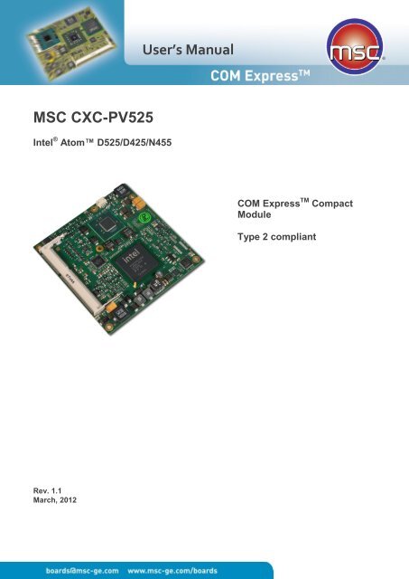
User's Manual MSC CXC-PV525 - MSC Vertriebs GmbH
User's Manual MSC CXC-PV525 - MSC Vertriebs GmbH
User's Manual MSC CXC-PV525 - MSC Vertriebs GmbH

You also want an ePaper? Increase the reach of your titles
YUMPU automatically turns print PDFs into web optimized ePapers that Google loves.
<strong>MSC</strong> <strong>CXC</strong>-<strong>PV525</strong><br />
Intel ® Atom D525/D425/N455<br />
Rev. 1.1<br />
March, 2012<br />
User’s <strong>Manual</strong><br />
COM Express TM Compact<br />
Module<br />
Type 2 compliant
<strong>MSC</strong> <strong>CXC</strong>-<strong>PV525</strong> <strong>User's</strong> <strong>Manual</strong><br />
Preface<br />
Copyright Notice<br />
Copyright © 2011 <strong>MSC</strong> <strong>Vertriebs</strong> <strong>GmbH</strong>. All rights reserved.<br />
Copying of this document, and giving it to others and the use or communication of the<br />
contents thereof, is forbidden without express authority. Offenders are liable to the payment<br />
of damages.<br />
All rights are reserved in the event of the grant of a patent or the registration of a utility model<br />
or design.<br />
Important Information<br />
This documentation is intended for qualified audience only. The product described herein is<br />
not an end user product. It was developed and manufactured for further processing by<br />
trained personnel.<br />
Disclaimer<br />
Although this document has been generated with the utmost care no warranty or liability for<br />
correctness or suitability for any particular purpose is implied. The information in this<br />
document is provided “as is” and is subject to change without notice.<br />
EMC Rules<br />
This unit has to be installed in a shielded housing. If not installed in a properly shielded<br />
enclosure, and used in accordance with the instruction manual, this product may cause radio<br />
interference in which case the user may be required to take adequate measures at his or her<br />
owns expense.<br />
Trademarks<br />
All used product names, logos or trademarks are property of their respective owners.<br />
Certification<br />
<strong>MSC</strong> <strong>Vertriebs</strong> <strong>GmbH</strong> is certified according to DIN EN ISO 9001:2000 standards.<br />
Life-Cycle-Management<br />
<strong>MSC</strong> products are developed and manufactured according to high quality standards. Our lifecycle-management<br />
assures long term availability through permanent product maintenance.<br />
Technically necessary changes and improvements are introduced if applicable. A product-<br />
change-notification and end-of-life management process assures early information of our<br />
customers.<br />
Product Support<br />
<strong>MSC</strong> engineers and technicians are committed to provide support to our customers<br />
whenever needed.<br />
Before contacting Technical Support of <strong>MSC</strong> <strong>Vertriebs</strong> <strong>GmbH</strong>, please consult the respective<br />
pages on our web site at www.msc-ge.com/support-boards for the latest documentation,<br />
drivers and software downloads.<br />
If the information provided there does not solve your problem, please contact our Technical<br />
Support:<br />
Email: support.boards@msc-ge.com<br />
Phone: +49 8165 906-200<br />
2
<strong>MSC</strong> <strong>CXC</strong>-<strong>PV525</strong> <strong>User's</strong> <strong>Manual</strong><br />
Content<br />
1 General Information ..................................................................................................... 5<br />
1.1 Revision History........................................................................................................ 5<br />
1.2 Reference Documents .............................................................................................. 5<br />
1.3 Introduction ............................................................................................................... 6<br />
2 Technical Description .................................................................................................. 7<br />
2.1 Key Features ............................................................................................................ 7<br />
2.2 Block diagram ........................................................................................................... 7<br />
2.3 Com Express Implementation ................................................................................... 8<br />
2.4 Functional Units ........................................................................................................ 9<br />
2.5 System Memory.......................................................................................................10<br />
2.6 Power Supply ..........................................................................................................10<br />
2.7 Current Dissipation ..................................................................................................10<br />
2.8 Mechanical Dimensions ...........................................................................................11<br />
2.8.1 Compact module ...............................................................................................11<br />
2.9 Thermal specifications .............................................................................................12<br />
2.9.1 Environment ......................................................................................................12<br />
2.10 Installation ............................................................................................................13<br />
2.10.1 Jumpers and switches ...................................................................................13<br />
2.10.2 Installing a DDR3 SO-DIMM module ..............................................................14<br />
2.10.3 Optional SATA NAND Flash ..........................................................................14<br />
2.11 Watchdog .............................................................................................................14<br />
2.12 Signal description .................................................................................................15<br />
2.12.1 High Definition Audio .....................................................................................15<br />
2.12.2 Ethernet .........................................................................................................15<br />
2.12.3 IDE ................................................................................................................16<br />
2.12.4 Serial ATA......................................................................................................16<br />
2.12.5 PCI Express Lanes ........................................................................................17<br />
2.12.6 PCI Express Lanes x16..................................................................................17<br />
2.12.7 Express Card Support ....................................................................................17<br />
2.12.8 PCI Bus .........................................................................................................18<br />
2.12.9 USB ...............................................................................................................19<br />
2.12.10 LVDS Flat Panel ............................................................................................19<br />
2.12.11 LPC Bus ........................................................................................................19<br />
2.12.12 Analog VGA ...................................................................................................20<br />
2.12.13 SPI Interface ..................................................................................................20<br />
2.12.14 Miscellaneous ................................................................................................20<br />
2.12.15 Power and System Management ...................................................................21<br />
2.12.16 General Purpose I/O ......................................................................................21<br />
2.12.17 Module Type Definition ..................................................................................22<br />
2.12.18 Power and GND .............................................................................................22<br />
2.13 Pin List for <strong>MSC</strong> <strong>CXC</strong>-<strong>PV525</strong> module (Type 2) ....................................................23<br />
3 System resources .......................................................................................................25<br />
3.1 PCI IRQ Routing ......................................................................................................25<br />
3.2 Carrier Board PCI Resource Allocation ....................................................................26<br />
3.3 SMB Address Map ...................................................................................................26<br />
4. Connectors ..............................................................................................................27<br />
4.2 Connector X5 (FAN) ................................................................................................27<br />
5. BIOS ........................................................................................................................28<br />
5.2 Introduction ..............................................................................................................28<br />
5.2.1 Startup Screen Overview ..................................................................................28<br />
5.2.2 Activity Detection Background ...........................................................................28<br />
5.3 TrustedCore Setup Utility .........................................................................................29<br />
5.3.1 Configuring the System BIOS............................................................................29<br />
5.3.2 The Main Menu .................................................................................................31<br />
3
<strong>MSC</strong> <strong>CXC</strong>-<strong>PV525</strong> <strong>User's</strong> <strong>Manual</strong><br />
5.3.2.1 Board Information .......................................................................................32<br />
5.3.2.2 Drive Settings .............................................................................................33<br />
5.3.2.3 Keyboard Features .....................................................................................34<br />
5.3.2.4 Boot Features .............................................................................................35<br />
5.3.3 The Advanced Menu .........................................................................................35<br />
5.3.3.1 Cache Memory ...........................................................................................37<br />
5.3.3.2 CPU Control Sub-Menu ..............................................................................37<br />
Note: Some options can be different dependent on used type of CPU ! ......................37<br />
5.3.3.3 Video (Intel IGD) Control Sub-Menu ...........................................................38<br />
5.3.3.4 ICH Control Sub Menu ................................................................................39<br />
5.3.3.5 PNP Configuration ......................................................................................41<br />
5.3.3.6 ACPI Control Sub-Menu .............................................................................42<br />
5.3.3.7 Integrated Device Control Sub-Menu ..........................................................43<br />
5.3.3.7.1 PCI Express Sub-Menu ..............................................................................44<br />
5.3.3.7.2 ICH USB Control Sub-Menu .......................................................................45<br />
5.3.3.8 I/O Device Configuration Menu ...................................................................45<br />
5.3.3.9 Clock Control Sub-Menu .............................................................................46<br />
5.3.3.10 Watchdog Options ......................................................................................46<br />
5.3.4 The Security Menu ............................................................................................48<br />
5.3.5 The Power Menu ...............................................................................................49<br />
5.3.5.1 Hardware Monitor .......................................................................................49<br />
5.3.6 The Boot Menu .................................................................................................50<br />
5.3.7 The Exit Menu ...................................................................................................51<br />
5.4 Bios Update .............................................................................................................52<br />
5.5 Bios Crisis Recovery ...............................................................................................52<br />
5.6 Diagnostics Postcodes ............................................................................................56<br />
5.6.1 Bootblock Bios Postcodes .................................................................................56<br />
5.6.2 System Bios Postcodes.....................................................................................56<br />
5.6.3 Memory Detection Postcodes ...........................................................................60<br />
5.6.4 ACPI Postcodes ................................................................................................60<br />
4
<strong>MSC</strong> <strong>CXC</strong>-<strong>PV525</strong> <strong>User's</strong> <strong>Manual</strong><br />
1 General Information<br />
1.1 Revision History<br />
Rev. Date Description<br />
1.0 28.10.2011 Final Revision<br />
1.1 13.03.2012 Marked the default setup values<br />
1.2 Reference Documents<br />
[1] COM Express Module Base Specification<br />
COM Express Revision 1.0<br />
Last update: July 10 th , 2005<br />
[2] PCI Local Bus Specification Rev. 2.1<br />
PCI21.PDF<br />
Last update: June 1 st , 1995<br />
http://www.pcisig.com<br />
[3] ATA/ATAPI-6 Specification<br />
d1410r3b.pdf<br />
http://www.t13.org/<br />
[4] Serial ATA Specification<br />
Serial ATA 1.0 gold.pdf<br />
Last update: August 29 th , 2002 Rev.1.0<br />
http://www.sata-io.org/<br />
[5] IEEE Std. 802.3-2002<br />
802.3-2002.pdf<br />
http://www.ieee.org<br />
[6] Universal Bus Specification<br />
usb_20.pdf<br />
Last update: April 27 th , 2000<br />
http://www.usb.org<br />
5
<strong>MSC</strong> <strong>CXC</strong>-<strong>PV525</strong> <strong>User's</strong> <strong>Manual</strong><br />
1.3 Introduction<br />
COM Express, an open specification of the PICMG (PCI Industrial Computer<br />
Manufacturer Group), is a module concept to bring PCI Express and other latest<br />
technologies like SATA, USB 2.0 and LVDS on a COM (Computer On Module).<br />
A COM Express module is plugged onto an application-specific base board similar to<br />
the ETX concept, but offers more options and a growth path to future CPU technologies.<br />
Utilizing different sizes, COM Express can be used for highly embedded solutions up<br />
to high performance platforms.<br />
The <strong>MSC</strong> <strong>CXC</strong>-<strong>PV525</strong> is based on Intel Atom TM CPUs N455, D425 and D525 with the<br />
Intel I/O Controller Hub 8 Mobile (ICH8M).<br />
These Intel Atom TM CPUs are on the Intel embedded roadmap of, which means that<br />
the processors are available long term.<br />
The <strong>CXC</strong>-<strong>PV525</strong> supports DDR3 memory modules. It provides two 204-pin SO-DIMM<br />
sockets providing the flexibility to configure the system up to 4GB of DDR3-DRAM.<br />
The integrated graphics controller contains a refresh of the 3 rd generation graphics core.<br />
An analog RGB and a single LVDS channel are supported by this GPU.<br />
For evaluation and design-in of the COM Express modules we provide evaluation<br />
baseboards and develop motherboards providing the interface infrastructure for the<br />
COM Express module offering PC type connectors for external access.<br />
Up to 440 pins of connectivity are available between COM Express modules and the<br />
Carrier Board. Legacy buses such as PCI, parallel ATA, LPC, HDA are supported as<br />
well as new high speed serial interconnects such as PCI Express, Serial ATA and<br />
Gigabit Ethernet.<br />
To enhance interoperability between COM Express modules and Carrier Boards, five<br />
common signaling configurations (pin-out types) have been defined to ease system<br />
integration.<br />
6
<strong>MSC</strong> <strong>CXC</strong>-<strong>PV525</strong> <strong>User's</strong> <strong>Manual</strong><br />
2 Technical Description<br />
2.1 Key Features<br />
The <strong>MSC</strong> <strong>CXC</strong>-<strong>PV525</strong> COM Express module is designed as a type 2 module.<br />
Key features include:<br />
Module size 95 mm x 95 mm<br />
18 mm ‘z’ height with heat-spreader (with 5 mm stack option)<br />
Dual 220 pin connector (440 pins)<br />
2x DDR3 SO-DIMM module<br />
Eight USB 2.0 ports; four shared over-current lines<br />
Three Serial ATA ports with data rates up to 3.0Gb/s (300MB/s)<br />
Five PCI Express x1 lanes<br />
Support pins for two Express Cards<br />
One single channel 18-bit LVDS interface<br />
Analog VGA<br />
High definition digital audio interface (external codec)<br />
GBit Ethernet interface<br />
LPC interface<br />
Four GPI pins<br />
Four GPO pins<br />
+6V to +18V primary power supply input<br />
+5V standby (optional) and 3.3V RTC power supply inputs<br />
32 bit PCI interface<br />
IDE port (to support legacy ATA devices such as CD-ROM drives and Compact Flash<br />
storage cards)<br />
TPM module (option, TPM 1.2, SLB9635)<br />
Automatic fan control<br />
On module SATA NAND flash (option)<br />
2.2 Block diagram<br />
7
<strong>MSC</strong> <strong>CXC</strong>-<strong>PV525</strong> <strong>User's</strong> <strong>Manual</strong><br />
2.3 Com Express Implementation<br />
COM Express required and optional features of pin-out type 2 are summarized in the<br />
following table. The features identified as minimum (Min.) shall be implemented by all<br />
modules. Features identified up to maximum (Max) may be additionally implemented by<br />
a module.<br />
The column <strong>MSC</strong> <strong>CXC</strong>-<strong>PV525</strong> shows the implemented features of the <strong>MSC</strong> module:<br />
Function Type 2<br />
Min / Max<br />
8<br />
<strong>MSC</strong> <strong>CXC</strong>-<br />
<strong>PV525</strong><br />
Note<br />
System I/O<br />
PCI Express Graphics<br />
(PEG)<br />
0 / 1 0<br />
PCI Express Lanes 0 - 5 1 / 6 5 x1 (Option 1 x4, 1 x1)<br />
PCI Express Lanes 16-31<br />
(same as PEG pins)<br />
0 / 16 0<br />
SDVO Channels 0 / 2 0<br />
LVDS Channels 0 / 2 1 1x single channel, 18 bit<br />
VGA Port 0 / 1 1<br />
TV-Out NA 0<br />
PATA Port 1 / 1 1<br />
SATA Ports 2 / 4 3<br />
(There are only two SATA<br />
ports available, when SSD<br />
option is used.)<br />
Digital Audio Interface 0 / 1 1 High Definition Audio<br />
USB 2.0 Ports 4 / 8 8<br />
LAN 0 (10/100Base-T min) 1 / 1 1 82567V Gigabit LAN<br />
PCI Bus - 32 Bit 1 / 1 1<br />
Express Card Support 1 / 2 2<br />
LPC Bus 1 / 1 1<br />
System Management<br />
General Purpose Inputs 4 / 4 4<br />
General Purpose Outputs 4 / 4 4<br />
SMBus 1 / 1 1<br />
I2C 1 / 1 1<br />
Watch Dog Timer 0 / 1 1<br />
Speaker Out 1 / 1 1<br />
External BIOS ROM<br />
support<br />
0 / 1 1<br />
Reset Functions 1 / 1 1<br />
Power Management<br />
Thermal Protection 0 / 1 1<br />
Battery Low Alarm 0 / 1 1<br />
Suspend 0 / 1 1<br />
Wake 0 / 2 2 WOL, PCI Wake<br />
Power Button Support 1 / 1 1<br />
Power Good 1 / 1 1<br />
Security<br />
TPM (on request) 0 / 0 1 TPM 1.2 module
<strong>MSC</strong> <strong>CXC</strong>-<strong>PV525</strong> <strong>User's</strong> <strong>Manual</strong><br />
2.4 Functional Units<br />
CPUs Intel ® Atom TM Processor soldered.<br />
D525, 1.8GHz, dual core, 400MHz GPU, DMI<br />
D425, 1.8GHz, single core, 400MHz GPU, DMI<br />
N455, 1.66GHz, single core, 200MHz GPU, DMI<br />
Chipset Intel ® 82801GBM ICH8 M<br />
Memory Two 204-pin DDR3 SO-DIMM sockets for up to 4GB (max. height<br />
1250mil = 31.75mm)<br />
SATA 3 SATA channels up to 300MByte/s each<br />
EIDE 1 Enhanced IDE port ATA/UDMA100<br />
USB 8 x USB 2.0<br />
COM Express Type 2 interface, fully compliant<br />
PCI Express Five channels PCIe x1<br />
PCI 32 Bit standard interface<br />
LPC Low Pin Count Bus for heritage interfaces<br />
Graphics Integrated Graphics Engine<br />
DirectX ® 9 compliant Pixel Shader 2.0<br />
MPEG2 Hardware Acceleration<br />
Video Memory Intel® Dynamic Video Memory Technology 4.0<br />
LCD Interface LVDS 1x18Bit, single channel, max. resolution 1.366 x 768<br />
CRT Interface max resolution 2.048 x 1.536 @ 60 Hz<br />
Ethernet 10/100/1000Base-TX (Intel® 82567V)<br />
Sound Interface High Definition Audio interface<br />
Watchdog Timer PIC12C509A generates reset (programmable, 1s … 255h)<br />
SATA Flash 1 optional SATA Flash disk, up to 16 GB,<br />
TPM (option) optional TPM module, TPM 1.2, SLB9635<br />
Fan Supply 3-pin header (12V)<br />
Real Time Clock integrated in ICH 8 M<br />
EDID-EEPROM on board EDID EEPROM, enable / disable via SETUP<br />
BIOS Phoenix BIOS in SPI Flash device<br />
EEPROM EEPROM for CMOS setup backup<br />
RTC / CMOS integrated in Intel 82801HEM ICH8 M, (typ. 2.7 µA)<br />
Battery external<br />
System Monitoring Voltage, Temperature, Fan<br />
1 reduces available SATA channels<br />
Core voltage<br />
12V (Vin)<br />
CPU thermal diode<br />
Memory temperature sensor<br />
Board temperature sensor<br />
Automatic Fan Control<br />
9
<strong>MSC</strong> <strong>CXC</strong>-<strong>PV525</strong> <strong>User's</strong> <strong>Manual</strong><br />
2.5 System Memory<br />
The <strong>MSC</strong> <strong>CXC</strong>-<strong>PV525</strong> CPU module provides two sockets for memory modules which have<br />
to meet the following demands:<br />
204pin unbuffered DDR3 SO-DIMM<br />
1.5V supply voltage<br />
DDR3-800 / PC3-6400 or faster<br />
Maximal module height: 30mm<br />
SPD (Serial Presence Detect) EEPROM<br />
2.6 Power Supply<br />
+12V primary power supply input<br />
+5V standby<br />
Option, is not required for module operation.<br />
If not present, customer has to make sure that the supply voltages which are<br />
generated on the carrier board are switched off during suspend states, so that no<br />
current from the carrier board’s signal lines can flow to the CPU board.<br />
3.3V RTC power supply<br />
Option, is not required for module operation.<br />
BIOS SETUP data is stored in a non volatile backup memory device (EEPROM),<br />
therefore configuration data will not get lost during power off (except for time and date<br />
information)<br />
Voltage Input range Current<br />
+12V +6.0V - 18.0 V See next table<br />
+5V Standby +4.75V - 5.25 V max. 2A<br />
+3V RTC power supply +2.0V - 3.3V max. 6µA<br />
2.7 Current Dissipation<br />
All measurements were made by plugging a <strong>MSC</strong> <strong>CXC</strong>-<strong>PV525</strong> module onto a <strong>MSC</strong> CX-<br />
EVA2 Baseboard with a multimeter connected to the +12V Line. The module was equipped<br />
with two 1GByte memory modules.<br />
Three tests were performed:<br />
1. Booting Dos 6.22 from an USB stick.<br />
2. Booting Microsoft Windows XP Professional SP3 from an SATA harddrive to the<br />
desktop.<br />
3. Booting Microsoft Windows XP Professional SP3 from an SATA harddrive and using<br />
BurnIn Test V4.0 to achieve 100% CPU load.<br />
Module (CPU) DOS Prompt Windows XP Idle 100% CPU load<br />
Intel® D525 0.86 A (10.3 W) 0.74 A (8.9 W) 1.01 A (12.1 W)<br />
Intel® D425 0.88 A (10.6 W) 0.77 A (9.2 W) 0.90 A (10.8 W)<br />
Intel® N455 0.73 A (8.8 W) 0.59 A (7.1 W) 0.73 A (8.8 W)<br />
10
<strong>MSC</strong> <strong>CXC</strong>-<strong>PV525</strong> <strong>User's</strong> <strong>Manual</strong><br />
2.8 Mechanical Dimensions<br />
2.8.1 Compact module<br />
There are two height options defined in the COM Express specification: 5mm and 8mm.<br />
The height option is defined by the connectors on the baseboard.<br />
11
<strong>MSC</strong> <strong>CXC</strong>-<strong>PV525</strong> <strong>User's</strong> <strong>Manual</strong><br />
2.9 Thermal specifications<br />
The cooling solution of a COM Express module is based on a heatspreader concept.<br />
A heatspreader is a metal plate (typically aluminium) mounted on the top of the module. The<br />
connection between this plate and the module components is typically done by thermal<br />
interface materials like phase change foils, gap pads and copper or aluminium blocks. A very<br />
good thermal conductivity is required in order to conduct the heat from the cpu and the<br />
chipset to the heatspreader plate.<br />
The heatspreader of the <strong>MSC</strong> module is thermally attached using phase change materials<br />
and small aluminium blocks filling the gap between cpu and chipset dies and the<br />
heatspreader plate.<br />
The heatspreader is not a heatsink! It is a defined thermal interface for the system<br />
designer with fixed mechanical dimensions, so it should be possible to change different<br />
module types without problems. There must be a cooling solution for the system. The surface<br />
temperature of the heatspreader should not exceed 60°C.<br />
Main issue for the thermal functionality of a system is that each device of the module is<br />
operated within its specified thermal values. The max values of CPU and chipset are 100°C,<br />
so there may be system implementations where the heatspreader temperature could be<br />
higher.<br />
Anyway, in this case it has to be validated that there are no thermal spec violations of any<br />
assembled part or integrated circuit over the system temperature range even at worst case<br />
conditions.<br />
For mounting instructions and ordering numbers of heatspreaders and complete cooling<br />
solutions for this product visit our support pages at http://www.msc-ge.com/support-boards.<br />
2.9.1 Environment<br />
Temperature 0 ... + 60°C (operating),<br />
-25 ... + 85°C (non operating)<br />
Humidity (rel.) 5 … 95 % (operating),<br />
5 … 95 % (non operating)<br />
12
<strong>MSC</strong> <strong>CXC</strong>-<strong>PV525</strong> <strong>User's</strong> <strong>Manual</strong><br />
2.10 Installation<br />
2.10.1 Jumpers and switches<br />
There are two jumpers available on the module.<br />
Clear RTC: By shorting the pins of this jumper, the RTC Clock is reset.<br />
Recovery: By shorting this jumper, the module forces BIOS recovery function.<br />
13
<strong>MSC</strong> <strong>CXC</strong>-<strong>PV525</strong> <strong>User's</strong> <strong>Manual</strong><br />
2.10.2 Installing a DDR3 SO-DIMM module<br />
The <strong>CXC</strong>-<strong>PV525</strong> board has two standard 204-pin SO-DIMM sockets for 1.5V DDR3-<br />
SDRAM SO-DIMM modules.<br />
Using both sockets:<br />
Do not combine different organized memory modules. Always use combinations like<br />
1Rx8 with 1Rx8 or 2Rx8 with 2Rx8.<br />
Note: SO-DIMM Module height should not exceed 1260 mil (= 32 mm)<br />
2.10.3 Optional SATA NAND Flash<br />
An on module SATA NAND Flash up to 16 GB can be assembled connected to one<br />
SATA port. There are only two SATA ports left, when SSD option is used.<br />
2.11 Watchdog<br />
The <strong>CXC</strong>- <strong>PV525</strong> board has a watchdog function implemented in a PIC Microcontroller.<br />
The watchdog can be enabled and configured in the BIOS Setup.<br />
If the watchdog is enabled a counter is started which generates a reset if it is not<br />
retriggered within a programmable time window.<br />
Possible watchdog delays: 1s, 5s, 10s, 30s (default), 1min, 5min, 10min, 30min<br />
Possible watchdog timeout: 0.4s, 1s, 5s, 10s, 30s (default), 1min, 5min, 10min<br />
The time delay starts as soon as it is enabled in the BIOS<br />
<strong>MSC</strong> provides a software API which gives the application software access to the<br />
Watchdog functionality if needed.<br />
14
<strong>MSC</strong> <strong>CXC</strong>-<strong>PV525</strong> <strong>User's</strong> <strong>Manual</strong><br />
2.12 Signal description<br />
Pins are marked in the following tables with the power rail associated with the pin, and, for<br />
input and I/O pins, with the input voltage tolerance. The pin power rail and the pin input<br />
voltage tolerance may be different. For example, the PCI group is defined as having a 3.3V<br />
power rail, meaning that the output signals will only be driven to 3.3V, but the pins are<br />
tolerant of 5V signals.<br />
An additional label, “Suspend”, indicates that the pin is active during suspend states (S3, S4,<br />
S5). If suspend modes are used, then care must be taken to avoid loading signals that are<br />
active during suspend to avoid excessive suspend mode current draw.<br />
2.12.1 High Definition Audio<br />
Signal Pin Type Signal Power Power PU/PD Description Source /<br />
Level Rail Tolerance<br />
Target<br />
AC_RST# Output CMOS 3.3V<br />
Sus.<br />
3.3V Reset output to CODEC, active low. ICH8M<br />
AC_SYNC Output CMOS 3.3V 3.3V 8k2 PU 48kHz fixed-rate, sample-<br />
ICH8M<br />
20k PD synchronization signal to the CODEC(s).<br />
AC_BITCLK Output CMOS 3.3V 3.3V 20k PD 24.00 MHz serial data clock generated<br />
by the ICH9-M<br />
ICH8M<br />
AC_SDOUT Output CMOS 3.3V 3.3V 20k PD Serial TDM data output to the CODEC. ICH8M<br />
AC_SDIN[0:2] Input CMOS 3.3V 3.3V 20k PD Serial TDM data inputs from up to 3 ICH8M<br />
Sus.<br />
CODECs.<br />
2.12.2 Ethernet<br />
Signal Pin<br />
Type<br />
GBE0_MDI[0:3]+ Input/<br />
GBE0_MDI[0:3]- Output<br />
Signal Power<br />
Level Rail<br />
Analog 3.3V<br />
Sus.<br />
Power<br />
Tolerance<br />
15<br />
PU/PD Description Source /<br />
Target<br />
Gigabit Ethernet Controller 0: Media<br />
Dependent Interface Differential<br />
Pairs 0,1,2,3. The MDI can operate<br />
in 1000, 100 and 10 Mbit / sec<br />
modes.<br />
82567V<br />
GBE0_ACT# Open CMOS 3.3V 3.3V<br />
MDI[0]+/- B1_DA+/-<br />
MDI[1]+/- B1_DB+/-<br />
MDI[2]+/- B1_DC+/-<br />
MDI[3]+/- B1_DD+/-<br />
Gigabit Ethernet Controller 0 activity 82567V<br />
Drain<br />
Sus.<br />
indicator, active low.<br />
GBE0_LINK# Open CMOS 3.3V 3.3V Gigabit Ethernet Controller 0 link 82567V<br />
Drain<br />
Sus.<br />
indicator, active low.<br />
GBE0_LINK100# Open CMOS 3.3V 3.3V Gigabit Ethernet Controller 0 100 82567V<br />
Drain<br />
Sus.<br />
Mbit / sec link indicator, active low.<br />
GBE0_LINK1000# Open CMOS 3.3V 3.3V Gigabit Ethernet Controller 0 1000 82567V<br />
Drain<br />
Sus.<br />
Mbit / sec link indicator, active low.<br />
GBE0_CTREF REF GND min<br />
3.3V max<br />
82567 (1000MBit) : 1,8V 82567V
<strong>MSC</strong> <strong>CXC</strong>-<strong>PV525</strong> <strong>User's</strong> <strong>Manual</strong><br />
2.12.3 IDE<br />
Signal Pin Signal Power Power PU/PD Description Source /<br />
Type Level Rail Tolerance<br />
Target<br />
IDE_D[0:6,8:15] I/O CMOS 3.3V 5V Bidirectional data to / from IDE device. ICH8M<br />
IDE_D[7] I/O CMOS 3.3V 5V 15k PD Bidirectional data to / from IDE device. ICH8M<br />
IDE_A[0:2] O CMOS 3.3V 3.3V Address lines to IDE device. ICH8M<br />
IDE_IOW# O CMOS 3.3V 3.3V I/O write line to IDE device. Data latched<br />
on trailing (rising) edge.<br />
ICH8M<br />
IDE_IOR# O CMOS 3.3V 3.3V I/O read line to IDE device. ICH8M<br />
IDE_REQ I CMOS 3.3V 5V 15k PD IDE Device DMA Request. It is asserted<br />
by the IDE device to request a data<br />
transfer.<br />
ICH8M<br />
IDE_ACK# O CMOS 3.3V 3.3V IDE Device DMA Acknowledge. ICH8M<br />
IDE_CS1# O CMOS 3.3V 3.3V IDE Device Chip Select for 1F0h to 1FFh<br />
range.<br />
ICH8M<br />
IDE_CS3# O CMOS 3.3V 3.3V IDE Device Chip Select for 3F0h to 3FFh<br />
range.<br />
ICH8M<br />
IDE_IORDY I CMOS 3.3V 5V 4k7 PU IDE device I/O ready input. Pulled low by<br />
the IDE device to extend the cycle.<br />
ICH8M<br />
IDE_RESET# O CMOS 3.3V<br />
Sus.<br />
3.3V Reset output to IDE device, active low.<br />
IDE_IRQ I CMOS 3.3V 5V 8k2 PU Interrupt request from IDE device. ICH8M<br />
IDE_CBLID# I CMOS 3.3V 3.3V 10k PD Input from off-module hardware indicating<br />
the type of IDE cable being used. High<br />
indicates a 40-pin cable used for legacy<br />
IDE modes. Low indicates that an 80-pin<br />
cable with interleaved grounds is used.<br />
Such a cable is required for Ultra-DMA 66,<br />
100 and 133 modes.<br />
ICH8M<br />
2.12.4 Serial ATA<br />
Signal Pin Signal Power Remark PU/PD Description Source /<br />
Type Level Rail<br />
Target<br />
SATA0_TX+ O SATA 3.3V AC coupled<br />
Serial ATA Channel 0 transmit differential pair. ICH8M<br />
SATA0_TX-<br />
on module<br />
SATA0_RX+ I SATA 3.3V AC coupled<br />
Serial ATA Channel 0 receive differential pair. ICH8M<br />
SATA0_RX-<br />
on module<br />
SATA1_TX+ O SATA 3.3V AC coupled<br />
Serial ATA Channel 0 transmit differential pair. ICH8M<br />
SATA1_TX-<br />
on module<br />
SATA1_RX+ I SATA 3.3V AC coupled<br />
Serial ATA Channel 0 receive differential pair. ICH8M<br />
SATA1_RX-<br />
on module<br />
SATA2_TX+ O SATA 3.3V AC coupled<br />
Serial ATA Channel 0 transmit differential pair. ICH8M<br />
SATA2_TX-<br />
on module<br />
SATA2_RX+ I SATA 3.3V AC coupled<br />
Serial ATA Channel 0 receive differential pair. ICH8M<br />
SATA2_RX-<br />
on module<br />
SATA3_TX+ O SATA 3.3V AC coupled<br />
Serial ATA Channel 0 transmit differential pair. ICH8M<br />
SATA3_TX-<br />
on module<br />
SATA3_RX+ I SATA 3.3V AC coupled<br />
Serial ATA Channel 0 receive differential pair. ICH8M<br />
SATA3_RX-<br />
on module<br />
ATA_ACT# O CMOS 3.3V 3.3V SATA activity indicator, active low.<br />
16
<strong>MSC</strong> <strong>CXC</strong>-<strong>PV525</strong> <strong>User's</strong> <strong>Manual</strong><br />
2.12.5 PCI Express Lanes<br />
Signal Pin Signal Power Remark /<br />
Type Level Rail Power Tol.<br />
PCIE_TX[0:4]+ O PCIe 3.3V AC coupled<br />
PCIE_TX[0:4]-<br />
on module<br />
PCIE_RX[0:4]+ I PCIe 3.3V AC coupled<br />
PCIE_RX[0:4]-<br />
off module<br />
PCIE_TX[5]+ O PCIe 3.3V AC coupled<br />
PCIE_TX[5]-<br />
on module<br />
PCIE_RX[5]+ I PCIe 3.3V AC coupled<br />
PCIE_RX[5]-<br />
off module<br />
PCIE_TX[16:31]+ O PCIe 3.3V AC coupled<br />
PCIE_TX[16:31]-<br />
on module<br />
PCIE_RX[16:31]+<br />
PCIE_RX[16:31]-<br />
PCIE_CLK_REF+<br />
PCIE_CLK_REF-<br />
I PCIe 3.3V AC coupled<br />
off module<br />
O PCIe<br />
CLK<br />
2.12.6 PCI Express Lanes x16<br />
Signal Pin<br />
Type<br />
PEG_TX[0:15]+<br />
PEG_TX[0:15]-<br />
PEG_RX[0:15]+<br />
PEG_RX[0:15]-<br />
Signal<br />
Level<br />
3.3V AC coupled<br />
on module<br />
Power<br />
Rail<br />
Remark<br />
/ Power<br />
Tol.<br />
O PCIe 3.3V AC<br />
coupled<br />
on<br />
module<br />
I PCIe 3.3V AC<br />
coupled<br />
off<br />
module<br />
PEG_LANE_RV# I CMOS 3.3V 3.3V 5k7<br />
PU<br />
PEG_ENABLE# I CMOS 3.3V 3.3V 100k<br />
PU<br />
2.12.7 Express Card Support<br />
PU/<br />
PD<br />
17<br />
Description Source /<br />
Target<br />
PCI Express Differential Transmit Pairs 0 ICH8M<br />
through 4<br />
PCI Express Differential Receive Pairs 0 ICH8M<br />
through 4<br />
PCI Express Differential Transmit Pair 5 not<br />
supported<br />
PCI Express Differential Receive Pair 5 not<br />
supported<br />
PCI Express Differential Transmit Pairs 16 not<br />
through 31. These are same lines as supported<br />
PEG_TX[0:15]+ and - in module pin-out<br />
types 4 and 5.<br />
PCI Express Differential Receive Pairs 16 not<br />
through 31. These are the same lines as supported<br />
PEG_RX[0:15]+ and - in module pin-out<br />
types 4 and 5.<br />
Reference clock output for all PCI Express CK505<br />
and PCI Express Graphics lanes.<br />
PU/PD Description Source /<br />
Target<br />
PCI Express Graphics transmit differential<br />
pairs. Some of these are multiplexed with<br />
SDVO lines (see SDVO section).<br />
These are the same lines as<br />
PCIE_TX[16:31]+ and - in module pin-out<br />
types 4 and 5.<br />
PCI Express Graphics receive differential<br />
pairs. Some of these are multiplexed with<br />
SDVO lines (see SDVO section).<br />
These are the same lines as<br />
PCIE_RX[16:31]+ and - in module pin-out<br />
types 4 and 5.<br />
PCI Express Graphics lane reversal input<br />
strap. Pull low on the carrier board to reverse<br />
lane order. Be aware that the SDVO lines that<br />
share this interface do not necessarily<br />
reverse order if this strap is low.<br />
Strap to enable PCI Express x16 external<br />
graphics interface. Pull low to disable internal<br />
graphics and enable the x16 interface.<br />
not<br />
supported<br />
not<br />
supported<br />
not<br />
supported<br />
not<br />
supported<br />
Signal Pin Signal Power Remark / PU/PD Description Source /<br />
Type Level Rail Power Tol.<br />
Target<br />
EXCD[0]_CPPE# I CMOS 3.3V 3.3V 8k2 PU ExpressCard card request, active<br />
low<br />
ICH8M<br />
EXCD[1]_CPPE# I CMOS 3.3V 3.3V ExpressCard card request, active not<br />
low<br />
supported<br />
EXCD[0]_RST# O CMOS 3.3V 3.3V 8k2 PU ExpressCard reset, active low ICH8M<br />
EXCD[1]_RST# O CMOS 3.3V 3.3V 8k2 PU ExpressCard reset, active low ICH8M
<strong>MSC</strong> <strong>CXC</strong>-<strong>PV525</strong> <strong>User's</strong> <strong>Manual</strong><br />
2.12.8 PCI Bus<br />
Signal Pin Signal Power Remark / PU/PD Description Source /<br />
Type Level Rail Power Tol.<br />
Target<br />
PCI_AD[0:31] I/O CMOS 3.3V 5V PCI bus multiplexed address and data<br />
lines<br />
ICH8M<br />
PCI_C/BE[0:3]# I/O CMOS 3.3V 5V PCI bus byte enable lines, active low ICH8M<br />
PCI_DEVSEL# I/O CMOS 3.3V 5V 8k2 PU PCI bus Device Select, active low. ICH8M<br />
PCI_FRAME# I/O CMOS 3.3V 5V 8k2 PU PCI bus Frame control line, active low. ICH8M<br />
PCI_IRDY# I/O CMOS 3.3V 5V 8k2 PU PCI bus Initiator Ready control line,<br />
active low.<br />
ICH8M<br />
PCI_TRDY# I/O CMOS 3.3V 5V 8k2 PU PCI bus Target Ready control line,<br />
active low.<br />
ICH8M<br />
PCI_STOP# I/O CMOS 3.3V 5V 8k2 PU PCI bus STOP control line, active low,<br />
driven by cycle initiator.<br />
ICH8M<br />
PCI_PAR I/O CMOS 3.3V 5V PCI bus parity ICH8M<br />
PCI_PERR# I/O CMOS 3.3V 5V 8k2 PU Parity Error: An external PCI device<br />
drives PERR# when it receives data<br />
that has a parity error.<br />
ICH8M<br />
PCI_REQ[0:3]# I CMOS 3.3V 5V 8k2 PU PCI bus master request input lines,<br />
active low.<br />
ICH8M<br />
PCI_GNT[0:3]# O CMOS 3.3V 5V PCI bus master grant output lines,<br />
active low.<br />
ICH8M<br />
PCI_RESET# O CMOS 3.3V<br />
Sus.<br />
5V PCI Reset output, active low. ICH8M<br />
PCI_LOCK# I/O CMOS 3.3V 5V 8k2 PU PCI Lock control line, active low. ICH8M<br />
PCI_SERR# I/O CMOS 3.3V 5V 8k2 PU System Error: SERR# may be pulsed ICH8M<br />
OD<br />
active by any PCI device that detects a<br />
system error condition.<br />
PCI_PME# I CMOS 3.3V 3.3V 20k PU PCI Power Management Event: PCI ICH8M<br />
Sus.<br />
peripherals drive PME# to wake<br />
system from low-power states S1–S5.<br />
PCI_CLKRUN# I/O CMOS 3.3V 3.3V 10k PU Bidirectional pin used to support PCI<br />
clock run protocol for mobile systems.<br />
ICH8M<br />
PCI_IRQ[A:D]# I CMOS 3.3V 5V 8k2 PU PCI interrupt request lines. ICH8M<br />
PCI_CLK O CMOS 3.3V 3.3V PCI 33MHz clock output. CK505<br />
PCI_M66EN I CMOS 3.3V 5V Module input signal indicates whether Not<br />
an off-module PCI device is capable of<br />
66MHz operation. Pulled to GND by<br />
Carrier Board device or by Slot Card if<br />
the devices are NOT capable of 66<br />
MHz operation.<br />
If the module is not capable of<br />
supporting 66 MHz PCI operation, this<br />
input may be a no-connect on the<br />
module.<br />
If the module is capable of supporting<br />
66 MHz PCI operation, and if this input<br />
is held low by the Carrier Board, the<br />
module PCI interface shall operate at<br />
33 MHz.<br />
supported<br />
18
<strong>MSC</strong> <strong>CXC</strong>-<strong>PV525</strong> <strong>User's</strong> <strong>Manual</strong><br />
2.12.9 USB<br />
Signal Pin<br />
Type<br />
Signal<br />
Level<br />
Power<br />
Rail<br />
USB[0:7]+ I/O USB 3.3V<br />
USB[0:7]-<br />
Sus.<br />
USB_0_1_OC# I CMOS 3.3V<br />
Sus.<br />
USB_2_3_OC# I CMOS 3.3V<br />
Sus.<br />
USB_4_5_OC# I CMOS 3.3V<br />
Sus.<br />
USB_6_7_OC# I CMOS 3.3V<br />
Sus.<br />
2.12.10 LVDS Flat Panel<br />
Remark /<br />
Power<br />
Tol.<br />
PU/<br />
PD<br />
3.3V 15k<br />
PD<br />
3.3V 8k2<br />
PU<br />
3.3V 8k2<br />
PU<br />
3.3V 8k2<br />
PU<br />
3.3V 8k2<br />
PU<br />
19<br />
Description Source /<br />
Target<br />
USB differential pairs, channels 0 through 7 ICH8M<br />
USB over-current sense, USB channels 0 and<br />
1. A pull-up for this line is present on the<br />
module. An open drain driver from a USB<br />
current monitor on the Carrier Board may<br />
drive this line low.<br />
Do not pull this line high on the Carrier Board.<br />
USB over-current sense, USB channels 2 and<br />
3. A pull-up for this line is present on the<br />
module. An open drain driver from a USB<br />
current monitor on the Carrier Board may<br />
drive this line low.<br />
Do not pull this line high on the Carrier Board.<br />
USB over-current sense, USB channels 4 and<br />
5. A pull-up for this line is present on the<br />
module. An open drain driver from a USB<br />
current monitor on the Carrier Board may<br />
drive this line low.<br />
Do not pull this line high on the Carrier Board.<br />
USB over-current sense, USB channels 6 and<br />
7. A pull-up for this line is present on the<br />
module. An open drain driver from a USB<br />
current monitor on the Carrier Board may<br />
drive this line low.<br />
Do not pull this line high on the Carrier Board.<br />
ICH8M<br />
ICH8M<br />
ICH8M<br />
ICH8M<br />
Signal Pin Signal Power Remark / PU/PD Description Source /<br />
Type Level Rail Power Tol.<br />
Target<br />
LVDS_A[0:3]+<br />
LVDS_A[0:3]-<br />
O LVDS LVDS Channel A differential pairs CPU<br />
LVDS_A_CK+<br />
LVDS_A_CK-<br />
O LVDS LVDS Channel A differential clock CPU<br />
LVDS_VDD_EN O CMOS 3.3V 3.3V 100k PD LVDS panel power enable CPU<br />
LVDS_BKLT_EN O CMOS 3.3V 3.3V 100k PD LVDS panel backlight enable CPU<br />
LVDS_BKLT_CTRL O CMOS 3.3V 3.3V 100k PD LVDS panel backlight brightness<br />
control<br />
CPU<br />
LVDS_I2C_CK O CMOS 3.3V 3.3V 8k2 PU I2C clock output for LVDS display<br />
use<br />
CPU<br />
LVDS_I2C_DAT I/O<br />
OD<br />
CMOS 3.3V 3.3V 8k2 PU I2C data line for LVDS display use CPU<br />
2.12.11 LPC Bus<br />
Signal Pin Signal Power Remark / PU/PD Description Source /<br />
Type Level Rail Power Tol.<br />
Target<br />
LPC_AD[0:3] I/O CMOS 3.3V 3.3V LPC multiplexed address, command and<br />
data bus<br />
ICH8M<br />
LPC_FRAME# O CMOS 3.3V 3.3V LPC frame indicates the start of an LPC<br />
cycle<br />
ICH8M<br />
LPC_DRQ[0:1]# I CMOS 3.3V 3.3V 20k PU LPC serial DMA request ICH8M<br />
LPC_SERIRQ I/O CMOS 3.3V 3.3V LPC serial interrupt ICH8M<br />
LPC_CLK O CMOS 3.3V 3.3V LPC clock output - 33MHz nominal CK505
<strong>MSC</strong> <strong>CXC</strong>-<strong>PV525</strong> <strong>User's</strong> <strong>Manual</strong><br />
2.12.12 Analog VGA<br />
Signal Pin Signal Power Remark / PU/P Description Source /<br />
Type Level Rail Power Tol. D<br />
Target<br />
VGA_RED O Analog 150R Red for monitor. Analog DAC output,<br />
CPU<br />
PD designed to drive a 37.5-Ohm equivalent<br />
load.<br />
VGA_GRN O Analog 150R Green for monitor. Analog DAC output, CPU<br />
PD designed to drive a 37.5-Ohm equivalent<br />
load.<br />
VGA_BLU O Analog 150R Blue for monitor. Analog DAC output,<br />
CPU<br />
PD designed to drive a 37.5-Ohm equivalent<br />
load.<br />
VGA_HSYNC O CMOS 3.3V 3.3V Horizontal sync output to VGA monitor CPU<br />
VGA_VSYNC O CMOS 3.3V 3.3V Vertical sync output to VGA monitor CPU<br />
VGA_I2C_CK O CMOS 3.3V 3.3V 2k2 DDC clock line (I2C port dedicated to identify CPU<br />
PU VGA monitor capabilities)<br />
VGA_I2C_DAT I/O CMOS 3.3V 3.3V 2k2 DDC data line. CPU<br />
OD<br />
PU<br />
2.12.13 SPI Interface<br />
Signal Pin Signal Power Rail Remark / PU/PD Description Source /<br />
Type Level<br />
Power Tol.<br />
Target<br />
SPI_CS# O CMOS 3.3V Sus. 3.3V Chip select for Carrier board SPI ICH8M<br />
SPI_MISO I CMOS 3.3V Sus. 3.3V 8k2 PU Data in to module from Carrier SPI ICH8M<br />
SPI_MOSI O CMOS 3.3V Sus. 3.3V 8k2 PU Data out from module to Carrier SPI ICH8M<br />
SPI_CLK O CMOS 3.3V Sus. 3.3V Clock from module to Carrier SPI ICH8M<br />
SPI_POWER O 3.3V Sus. 3.3V Power supply for Carrier Board SPI<br />
BIOS_DIS0# I CMOS 3.3V Sus. 3.3V 4k7 PU Selection strap to determine the BIOS<br />
boot device<br />
Boot BIOS destination select<br />
0 - LPC/FWH<br />
1 - SPI<br />
ICH8M<br />
BIOS_DIS1# I CMOS 3.3V Sus. 3.3V Selection strap to determine the BIOS<br />
boot device<br />
2.12.14 Miscellaneous<br />
20<br />
Not<br />
supported<br />
Signal Pin Signal Power Remark / PU/PD Description Source /<br />
Type Level Rail Power Tol.<br />
Target<br />
I2C_CK O CMOS 3.3V 3.3V 2k2 PU General purpose I2C port clock output ICH8M<br />
I2C_DAT I/O CMOS 3.3V 3.3V 2k2 PU General purpose I2C port data I/O line ICH8M<br />
SPKR O CMOS 3.3V 3.3V 20k PD Output for audio enunciator - the "speaker"<br />
in PC-AT systems<br />
ICH8M<br />
BIOS_DISABLE# I CMOS 3.3V 3.3V 4k7 PU Module BIOS disable input. Pull low to Disables<br />
Sus.<br />
disable module BIOS.<br />
SPI<br />
Flash<br />
WDT O CMOS 3.3V 3.3V 10k PU Output indicating that a watchdog time-out PIC12C5<br />
event has occurred.<br />
09<br />
KBD_RST# I CMOS 3.3V 3.3V 10k PU Input to module from (optional) external<br />
keyboard controller that can force a reset.<br />
Pulled high on the module. This is a legacy<br />
artifact of the PC-AT.<br />
ICH8M<br />
KBD_A20GATE CMOS 3.3V 3.3V 10k PU Input to module from (optional) external<br />
keyboard controller that can be used to<br />
control the CPU A20 gate line. The<br />
A20GATE restricts the memory access to<br />
the bottom megabyte and is a legacy<br />
artifact of the PC- AT. Pulled high on the<br />
module.<br />
ICH8M
<strong>MSC</strong> <strong>CXC</strong>-<strong>PV525</strong> <strong>User's</strong> <strong>Manual</strong><br />
2.12.15 Power and System Management<br />
Signal Pin Signal Power Remark / PU/PD Description Source /<br />
Type Level Rail Power Tol.<br />
Target<br />
PWRBTN# I CMOS 3.3V 3.3V 10k PU Power button to bring system out of<br />
ICH8M<br />
Sus.<br />
Suspend states, active on falling edge.<br />
SYS_RESET# I CMOS 3.3V 3.3V 10k PU Reset button input. Active low input. System ICH8M<br />
Sus.<br />
is held in hardware reset while this input is<br />
low, and comes out of reset upon release.<br />
CB_RESET# O CMOS 3.3V 3.3V Reset output from module to Carrier Board. ICH8M<br />
Sus.<br />
Active low. Issued by module chipset and<br />
may result from a low SYS_RESET# input, a<br />
low PWR_OK input, a VCC_12V power input<br />
that falls below the minimum specification, a<br />
watchdog timeout, or may be initiated by the<br />
module software.<br />
PWR_OK I CMOS 3.3V 3.3V 220k Power OK from main power supply. A high Power<br />
Sus.<br />
PU value indicates that the power is good. Good<br />
logic<br />
SUS_STAT# O CMOS 3.3V 3.3V Indicates imminent suspend operation; used ICH8M<br />
Sus.<br />
to notify LPC devices.<br />
SUS_S3# O CMOS 3.3V 3.3V Indicates system is in Suspend to RAM ICH8M<br />
Sus.<br />
state. Active low output.<br />
SUS_S4# O CMOS 3.3V 3.3V Indicates system is in Suspend to Disk state. ICH8M<br />
Sus.<br />
Active low output.<br />
SUS_S5# O CMOS 3.3V 3.3V Indicates system is in Soft Off state. Also ICH8M<br />
Sus.<br />
known as "PS_ON" and can be used to<br />
control an ATX power supply.<br />
WAKE0# I CMOS 3.3V<br />
Sus.<br />
3.3V 1k PU PCI Express wake up signal. ICH8M<br />
WAKE1# I CMOS 3.3V 3.3V 1k PU General purpose wake up signal. May be ICH8M<br />
Sus.<br />
used to implement wake-up on PS2<br />
keyboard or mouse activity.<br />
BATLOW# I CMOS 3.3V<br />
Sus.<br />
3.3V 10k PU Indicates that external battery is low. ICH8M<br />
THRM# I CMOS 3.3V 3.3V 10k PU Input from off-module temp sensor indicating ICH8M<br />
Sus.<br />
an over-temp situation.<br />
THERMTRIP# O CMOS 3.3V 3.3V 330R Active low output indicating that the CPU CPU<br />
PU has entered thermal shutdown.<br />
SMB_CK I/O CMOS 3.3V 3.3V Act. PU System Management Bus bidirectional clock ICH8M<br />
OD<br />
Sus.<br />
line. Power sourced through 5V standby rail<br />
and main power rails.<br />
SMB_DAT I/O CMOS 3.3V 3.3V Act. PU System Management Bus bidirectional data ICH8M<br />
OD<br />
Sus.<br />
line. Power sourced through 5V standby rail<br />
and main power rails.<br />
SMB_ALERT# I CMOS 3.3V 3.3V 10k PU System Management Bus Alert – active low ICH8M<br />
Sus.<br />
input can be used to generate an SMI#<br />
(System Management Interrupt) or to wake<br />
the system. Power sourced through 5V<br />
standby rail and main power rails.<br />
2.12.16 General Purpose I/O<br />
Signal Pin Signal Power Remark / PU/PD Description Source /<br />
Type Level Rail Power Tol.<br />
Target<br />
GPO[1..2] O CMOS 3.3V 3.3V General purpose output pins. ICH8M<br />
GPO0 O CMOS 3.3V 3.3V 10k PD General purpose output pins. ICH8M<br />
GPO3 O CMOS 3.3V 3.3V 10k PD General purpose output pins. ICH8M<br />
GPI[0:3] I CMOS 3.3V 3.3V General purpose input pins. ICH8M<br />
21
<strong>MSC</strong> <strong>CXC</strong>-<strong>PV525</strong> <strong>User's</strong> <strong>Manual</strong><br />
2.12.17 Module Type Definition<br />
Signal Pin<br />
Type<br />
TYPE[0:2]# Type<br />
Detect<br />
Signal<br />
Level<br />
Power<br />
Rail<br />
2.12.18 Power and GND<br />
Remark /<br />
Power Tol.<br />
PU/PD Description Source /<br />
Target<br />
The TYPE pins indicate to the Carrier Board For this<br />
the Pin-out Type that is implemented on the Type 2<br />
module. The pins are tied on the module to board, all<br />
either ground (GND) 22 rare no-connects Type<br />
(NC). For Pin-out Type 1, these pins are don’t Detect<br />
care (X).<br />
pins are<br />
n.c.<br />
TYPE2# TYPE1# TYPE0#<br />
X<br />
Type 1<br />
X X Pin-out<br />
NC<br />
Type 2<br />
NC NC Pin-out<br />
NC NC GND Pin-out<br />
Type 3 (no IDE)<br />
NC GND NC Pin-out<br />
Type 4 (no PCI)<br />
NC GND GND Pin-out<br />
Type 5 (no IDE, no PCI)<br />
22<br />
The Carrier Board should implement<br />
combinatorial logic that monitors the module<br />
TYPE pins and keeps power off (e.g<br />
deactivates the ATX_ON signal for an ATX<br />
power supply) if an incompatible module pin-<br />
out type is detected. The Carrier Board logic<br />
may also implement a fault indicator such as a<br />
LED.<br />
Signal Pin Signal Power Remark / PU/PD Description Source /<br />
Type Level Rail Power Tol.<br />
Target<br />
VCC_12V Power 12V<br />
Primary power input: +6V - +18V Voltage<br />
(±5%)<br />
Regulators<br />
VCC_5V_SBY Power 5V<br />
Standby power input: +5.0V (±5%) VCC3.3V<br />
(±5%)<br />
If VCC5_SBY is used, all available SUS<br />
VCC_5V_SBY pins on the connector(s)<br />
shall be used.<br />
Only used for standby and suspend<br />
functions.<br />
May be left unconnected if these<br />
functions are not used in the system<br />
design.<br />
regulator<br />
VCC_RTC Power Real-time clock circuit-power input :<br />
+3.0V (+2.0V to +3.3V)<br />
ICH8M<br />
GND Power Ground - DC power and signal and AC<br />
signal return path. All available GND<br />
connector pins shall be used and tied to<br />
Carrier Board GND plane.
<strong>MSC</strong> <strong>CXC</strong>-<strong>PV525</strong> <strong>User's</strong> <strong>Manual</strong><br />
2.13 Pin List for <strong>MSC</strong> <strong>CXC</strong>-<strong>PV525</strong> module (Type 2)<br />
Row A Row B Row C Row D<br />
A1 GND (FIXED) B1 GND (FIXED) C1 GND (FIXED) D1 GND (FIXED)<br />
A2 GBE0_MDI3- B2 GBE0_ACT# C2 IDE_D7 D2 IDE_D5<br />
A3 GBE0_MDI3+ B3 LPC_FRAME# C3 IDE_D6 D3 IDE_D10<br />
A4 GBE0_LINK100# B4 LPC_AD0 C4 IDE_D3 D4 IDE_D11<br />
A5 GBE0_LINK1000# B5 LPC_AD1 C5 IDE_D15 D5 IDE_D12<br />
A6 GBE0_MDI2- B6 LPC_AD2 C6 IDE_D8 D6 IDE_D4<br />
A7 GBE0_MDI2+ B7 LPC_AD3 C7 IDE_D9 D7 IDE_D0<br />
A8 GBE0_LINK# B8 LPC_DRQ0# C8 IDE_D2 D8 IDE_REQ<br />
A9 GBE0_MDI1- B9 LPC_DRQ1# C9 IDE_D13 D9 IDE_IOW#<br />
A10 GBE0_MDI1+ B10 LPC_CLK C10 IDE_D1 D10 IDE_ACK#<br />
A11 GND (FIXED) B11 GND (FIXED) C11 GND (FIXED) D11 GND (FIXED)<br />
A12 GBE0_MDI0- B12 PWRBTN# C12 IDE_D14 D12 IDE_IRQ<br />
A13 GBE0_MDI0+ B13 SMB_CK C13 IDE_IORDY D13 IDE_A0<br />
A14 GBE0_CTREF B14 SMB_DAT C14 IDE_IOR# D14 IDE_A1<br />
A15 SUS_S3# B15 SMB_ALERT# C15 PCI_PME# D15 IDE_A2<br />
A16 SATA0_TX+ B16 SATA1_TX+ C16 PCI_GNT2# D16 IDE_CS1#<br />
A17 SATA0_TX- B17 SATA1_TX- C17 PCI_REQ2# D17 IDE_CS3#<br />
A18 SUS_S4# B18 SUS_STAT# C18 PCI_GNT1# D18 IDE_RESET#<br />
A19 SATA0_RX+ B19 SATA1_RX+ C19 PCI_REQ1# D19 PCI_GNT3#<br />
A20 SATA0_RX- B20 SATA1_RX- C20 PCI_GNT0# D20 PCI_REQ3#<br />
A21 GND (FIXED) B21 GND (FIXED) C21 GND (FIXED) D21 GND (FIXED)<br />
A22 SATA2_TX+ B22 SATA3_TX+ C22 PCI_REQ0# D22 PCI_AD1<br />
A23 SATA2_TX- B23 SATA3_TX- C23 PCI_RESET# D23 PCI_AD3<br />
A24 SUS_S5# B24 PWR_OK C24 PCI_AD0 D24 PCI_AD5<br />
A25 SATA2_RX+ B25 SATA3_RX+ C25 PCI_AD2 D25 PCI_AD7<br />
A26 SATA2_RX- B26 SATA3_RX- C26 PCI_AD4 D26 PCI_C/BE0#<br />
A27 BATLOW# B27 WDT C27 PCI_AD6 D27 PCI_AD9<br />
A28 ATA_ACT# B28 AC_SDIN2 C28 PCI_AD8 D28 PCI_AD11<br />
A29 AC_SYNC B29 AC_SDIN1 C29 PCI_AD10 D29 PCI_AD13<br />
A30 AC_RST# B30 AC_SDIN0 C30 PCI_AD12 D30 PCI_AD15<br />
A31 GND (FIXED) B31 GND (FIXED) C31 GND (FIXED) D31 GND (FIXED)<br />
A32 AC_BITCLK B32 SPKR C32 PCI_AD14 D32 PCI_PAR<br />
A33 AC_SDOUT B33 I2C_CK C33 PCI_C/BE1# D33 PCI_SERR#<br />
A34 BIOS_DIS0# B34 I2C_DAT C34 PCI_PERR# D34 PCI_STOP#<br />
A35 THRMTRIP# B35 THRM# C35 PCI_LOCK# D35 PCI_TRDY#<br />
A36 USB6- B36 USB7- C36 PCI_DEVSEL# D36 PCI_FRAME#<br />
A37 USB6+ B37 USB7+ C37 PCI_IRDY# D37 PCI_AD16<br />
A38 USB_6_7_OC# B38 USB_4_5_OC# C38 PCI_C/BE2# D38 PCI_AD18<br />
A39 USB4- B39 USB5- C39 PCI_AD17 D39 PCI_AD20<br />
A40 USB4+ B40 USB5+ C40 PCI_AD19 D40 PCI_AD22<br />
A41 GND (FIXED) B41 GND (FIXED) C41 GND (FIXED) D41 GND (FIXED)<br />
A42 USB2- B42 USB3- C42 PCI_AD21 D42 PCI_AD24<br />
A43 USB2+ B43 USB3+ C43 PCI_AD23 D43 PCI_AD26<br />
A44 USB_2_3_OC# B44 USB_0_1_OC# C44 PCI_C/BE3# D44 PCI_AD28<br />
A45 USB0- B45 USB1- C45 PCI_AD25 D45 PCI_AD30<br />
A46 USB0+ B46 USB1+ C46 PCI_AD27 D46 PCI_IRQC#<br />
A47 VCC_RTC B47 EXCD1_PERST# C47 PCI_AD29 D47 PCI_IRQD#<br />
A48 EXCD0_PERST# B48 EXCD1_CPPE# C48 PCI_AD31 D48 PCI_CLKRUN#<br />
A49 EXCD0_CPPE# B49 SYS_RESET# C49 PCI_IRQA# D49 PCI_M66EN<br />
A50 LPC_SERIRQ B50 CB_RESET# C50 PCI_IRQB# D50 PCI_CLK<br />
= not supported on <strong>MSC</strong> <strong>CXC</strong>-<strong>PV525</strong> module<br />
23
<strong>MSC</strong> <strong>CXC</strong>-<strong>PV525</strong> <strong>User's</strong> <strong>Manual</strong><br />
Row A Row B Row C Row D<br />
A51 GND (FIXED) B51 GND (FIXED) C51 GND (FIXED) D51 GND (FIXED)<br />
A52 PCIE_TX5+ B52 PCIE_RX5+ C52 PEG_RX0+ D52 PEG_TX0+<br />
A53 PCIE_TX5- B53 PCIE_RX5- C53 PEG_RX0- D53 PEG_TX0-<br />
A54 GPI0 B54 GPO1 C54 TYPE0# D54 PEG_LANE_RV#<br />
A55 PCIE_TX4+ B55 PCIE_RX4+ C55 PEG_RX1+ D55 PEG_TX1+<br />
A56 PCIE_TX4- B56 PCIE_RX4- C56 PEG_RX1- D56 PEG_TX1-<br />
A57 GND B57 GPO2 C57 TYPE1# D57 TYPE2#<br />
A58 PCIE_TX3+ B58 PCIE_RX3+ C58 PEG_RX2+ D58 PEG_TX2+<br />
A59 PCIE_TX3- B59 PCIE_RX3- C59 PEG_RX2- D59 PEG_TX2-<br />
A60 GND (FIXED) B60 GND (FIXED) C60 GND (FIXED) D60 GND (FIXED)<br />
A61 PCIE_TX2+ B61 PCIE_RX2+ C61 PEG_RX3+ D61 PEG_TX3+<br />
A62 PCIE_TX2- B62 PCIE_RX2- C62 PEG_RX3- D62 PEG_TX3-<br />
A63 GPI1 B63 GPO3 C63 RSVD D63 RSVD<br />
A64 PCIE_TX1+ B64 PCIE_RX1+ C64 RSVD D64 RSVD<br />
A65 PCIE_TX1- B65 PCIE_RX1- C65 PEG_RX4+ D65 PEG_TX4+<br />
A66 GND B66 WAKE0# C66 PEG_RX4- D66 PEG_TX4-<br />
A67 GPI2 B67 WAKE1# C67 RSVD D67 GND<br />
A68 PCIE_TX0+ B68 PCIE_RX0+ C68 PEG_RX5+ D68 PEG_TX5+<br />
A69 PCIE_TX0- B69 PCIE_RX0- C69 PEG_RX5- D69 PEG_TX5-<br />
A70 GND (FIXED) B70 GND (FIXED) C70 GND (FIXED) D70 GND (FIXED)<br />
A71 LVDS_A0+ B71 LVDS_B0+ C71 PEG_RX6+ D71 PEG_TX6+<br />
A72 LVDS_A0- B72 LVDS_B0- C72 PEG_RX6- D72 PEG_TX6-<br />
A73 LVDS_A1+ B73 LVDS_B1+ C73 SDVO_DATA D73 SDVO_CLK<br />
A74 LVDS_A1- B74 LVDS_B1- C74 PEG_RX7+ D74 PEG_TX7+<br />
A75 LVDS_A2+ B75 LVDS_B2+ C75 PEG_RX7- D75 PEG_TX7-<br />
A76 LVDS_A2- B76 LVDS_B2- C76 GND D76 GND<br />
A77 LVDS_VDD_EN B77 LVDS_B3+ C77 RSVD D77 IDE_CBLID#<br />
A78 LVDS_A3+ B78 LVDS_B3- C78 PEG_RX8+ D78 PEG_TX8+<br />
A79 LVDS_A3- B79 LVDS_BKLT_EN C79 PEG_RX8- D79 PEG_TX8-<br />
A80 GND (FIXED) B80 GND (FIXED) C80 GND (FIXED) D80 GND (FIXED)<br />
A81 LVDS_A_CK+ B81 LVDS_B_CK+ C81 PEG_RX9+ D81 PEG_TX9+<br />
A82 LVDS_A_CK- B82 LVDS_B_CK- C82 PEG_RX9- D82 PEG_TX9-<br />
A83 LVDS_I2C_CK B83 LVDS_BKLT_CTRL C83 RSVD D83 RSVD<br />
A84 LVDS_I2C_DAT B84 VCC_5V_SBY C84 GND D84 GND<br />
A85 GPI3 B85 VCC_5V_SBY C85 PEG_RX10+ D85 PEG_TX10+<br />
A86 KBD_RST# B86 VCC_5V_SBY C86 PEG_RX10- D86 PEG_TX10-<br />
A87 KBD_A20GATE B87 VCC_5V_SBY C87 GND D87 GND<br />
A88 PCIE0_CK_REF+ B88 BIOS_DIS1# C88 PEG_RX11+ D88 PEG_TX11+<br />
A89 PCIE0_CK_REF- B89 VGA_RED C89 PEG_RX11- D89 PEG_TX11-<br />
A90 GND (FIXED) B90 GND (FIXED) C90 GND (FIXED) D90 GND (FIXED)<br />
A91 SPI_POWER B91 VGA_GRN C91 PEG_RX12+ D91 PEG_TX12+<br />
A92 SPI_MISO B92 VGA_BLU C92 PEG_RX12- D92 PEG_TX12-<br />
A93 GPO0 B93 VGA_HSYNC C93 GND D93 GND<br />
A94 SPI_CLK B94 VGA_VSYNC C94 PEG_RX13+ D94 PEG_TX13+<br />
A95 SPI_MOSI B95 VGA_I2C_CK C95 PEG_RX13- D95 PEG_TX13-<br />
A96 GND B96 VGA_I2C_DAT C96 GND D96 GND<br />
A97 Type 10 VCC_12V B97 SPI_CS# C97 RSVD D97 PEG_ENABLE#<br />
A98 RSVD VCC_12V B98 RSVD C98 PEG_RX14+ D98 PEG_TX14+<br />
A99 RSVD VCC_12V B99 RSVD C99 PEG_RX14- D99 PEG_TX14-<br />
A100 GND (FIXED) B100 GND (FIXED) C100 GND (FIXED) D100 GND (FIXED)<br />
A101 RSVD VCC_12V B101 RSVD VCC_12V C101 PEG_RX15+ D101 PEG_TX15+<br />
A102 RSVD VCC_12V B102 RSVD VCC_12V C102 PEG_RX15- D102 PEG_TX15-<br />
A103 RSVD VCC_12V B103 RSVD VCC_12V C103 GND D103 GND<br />
A104 VCC_12V B104 VCC_12V C104 VCC_12V D104 VCC_12V<br />
A105 VCC_12V B105 VCC_12V C105 VCC_12V D105 VCC_12V<br />
A106 VCC_12V B106 VCC_12V C106 VCC_12V D106 VCC_12V<br />
A107 VCC_12V B107 VCC_12V C107 VCC_12V D107 VCC_12V<br />
A108 VCC_12V B108 VCC_12V C108 VCC_12V D108 VCC_12V<br />
A109 VCC_12V B109 VCC_12V C109 VCC_12V D109 VCC_12V<br />
A110 GND (FIXED) B110 GND (FIXED) C110 GND (FIXED) D110 GND (FIXED)<br />
= not supported on <strong>MSC</strong> <strong>CXC</strong>-<strong>PV525</strong> module<br />
24
<strong>MSC</strong> <strong>CXC</strong>-<strong>PV525</strong> <strong>User's</strong> <strong>Manual</strong><br />
3 System resources<br />
3.1 PCI IRQ Routing<br />
4<br />
Slot Number<br />
(or Onboard Device)<br />
IDSEL #<br />
or<br />
DEV. #<br />
Bus #<br />
PIRQ 0<br />
(INT A)<br />
25<br />
Interrupts of Controller (ICH-8M)<br />
PIRQ 1<br />
(INT B)<br />
Internal Graphic Dev 2 Fn 0 0 A<br />
GBit LAN Controller Dev 19 Fn 0 0 A<br />
UHCI (USB1.1) Host<br />
USB Ports 0,1<br />
USB Ports 2,3<br />
USB Ports 4,5<br />
USB Ports 6,7<br />
EHCI (USB2.0) Host<br />
USB Ports 0-5<br />
USB Ports 6-7<br />
Dev 29 Fn 0<br />
Dev 29 Fn 1<br />
Dev 29 Fn 2<br />
Dev 26 Fn 0<br />
0<br />
0<br />
0<br />
0<br />
A<br />
PIRQ 2<br />
(INT C)<br />
B<br />
A<br />
PIRQ 3<br />
(INT D)<br />
C<br />
PIRQ 4<br />
(INT E)<br />
PIRQ 5<br />
(INT F)<br />
PIRQ 6<br />
(INT G)<br />
Dev 29 Fn 7 0<br />
A<br />
Dev 26 Fn 7 0 C<br />
HD Audio<br />
PCIe x1 Root Port<br />
Dev 27 Fn 0 0 A<br />
for Slot 1<br />
Dev 28 Fn 0 0 A<br />
for Slot 2<br />
Dev 28 Fn 1 0<br />
B<br />
for Slot 3<br />
Dev 28 Fn 2 0<br />
C<br />
for Slot 4<br />
Dev 28 Fn 3 0<br />
D<br />
for Slot 5<br />
Dev 28 Fn 4 0 A<br />
SATA Controller Dev 31 Fn 2 0 B<br />
SMBus Controller Dev 31 Fn 3 0 C<br />
PCIe x1 Slot 1 Dev 0 Fn 0 dyn A B C D<br />
PCIe x1 Slot 2 Dev 0 Fn 0 dyn D A B C<br />
PCIe x1 Slot 3 Dev 0 Fn 0 dyn C D A B<br />
PCIe x1 Slot 4 Dev 0 Fn 0 dyn B C D A<br />
PCIe x1 Slot 5 Dev 0 Fn 0 dyn A B C D<br />
PCI Slot 1 AD20 / Dev 4 dyn A B C D<br />
PCI Slot 2 AD21 / Dev 5 dyn D A B C<br />
PCI Slot 3 AD22 / Dev 6 dyn C D A B<br />
PCI Slot 4 AD23 / Dev 7 dyn B C D A<br />
PATA Controller Dev 1F Fn 1 dyn A<br />
PIRQ 7<br />
(INT H)
<strong>MSC</strong> <strong>CXC</strong>-<strong>PV525</strong> <strong>User's</strong> <strong>Manual</strong><br />
3.2 Carrier Board PCI Resource Allocation<br />
The external PCI resource allocation on the carrier board should be as follows:<br />
The signals PCI_IRQx, PCI_REQx or PCI_GNTx are are routed exclusively to the COM<br />
Express connector. They are not shared on the CPU board.<br />
3.3 SMB Address Map<br />
Device A6 A5 A4 A3 A2 A1 A0 R/W address *)<br />
SMBus host (ICH8-M slave) 0 0 0 1 0 0 0 x 10h / 08h<br />
S<strong>MSC</strong> EMC2104 0 1 0 1 1 1 1 x 5Eh / 2Fh<br />
Watchdog (PIC12C509) 1 0 1 1 0 0 0 x B0h / 58h<br />
ICS9LPRS365 Clock Synthesizer 1 1 0 1 0 0 1 x D2h / 69h<br />
CMOS backup EEPROM 1 0 1 0 1 0 0 x A8h / 54h<br />
SPD EEPROM (SO-DIMM) 1 0 1 0 0 0 0 x A0h / 50h<br />
*) 8 bit address (with R/W) / 7 bit address (without R/W)<br />
26
<strong>MSC</strong> <strong>CXC</strong>-<strong>PV525</strong> <strong>User's</strong> <strong>Manual</strong><br />
4. Connectors<br />
4.2 Connector X5 (FAN)<br />
Pin Signal<br />
1 GND<br />
2 PWM controlled VCC +12V<br />
3 Fan speed<br />
Connector: JST S3B-ZR-SM4A-TF<br />
27
<strong>MSC</strong> <strong>CXC</strong>-<strong>PV525</strong> <strong>User's</strong> <strong>Manual</strong><br />
5. BIOS<br />
5.2 Introduction<br />
This guide describes the Phoenix TrustedCore Startup screen and contains information<br />
on how to access Phoenix TrustedCore setup to modify the settings which control<br />
Phoenix pre-OS (operating system) functions.<br />
5.2.1 Startup Screen Overview<br />
The Phoenix TrustedCore Startup screen is a graphical user interface (GUI) that is<br />
included in Phoenix TrustedCore products. The default bios behavior is to show an<br />
informational text screen during bios POST phase, but the graphical boot screen can be<br />
enabled in the bios setup. The standard boot screen is a black screen, including a<br />
progress bar at the bottom of the screen. This bar indicates the progress of the Startup<br />
Screen functions and provides user prompting and POST status. The following figure<br />
shows the various parts of a generic Startup Screen at 1024x768 resolution:<br />
5.2.2 Activity Detection Background<br />
While the TrustedCore Startup screen is displayed, press the Setup Entry key (F2 –<br />
TrustedCore default). The TrustedCore Startup Status Bar acknowledges the input, and<br />
at the end of POST, the screen clears and setup launches.<br />
An example of the Startup Status Bar displaying changing state is shown in the following<br />
figure. The “Please Wait…” text is displayed after the F2 key is pressed to acknowledge<br />
user input.<br />
Active status bar:<br />
28
<strong>MSC</strong> <strong>CXC</strong>-<strong>PV525</strong> <strong>User's</strong> <strong>Manual</strong><br />
5.3 TrustedCore Setup Utility<br />
With the Phoenix TrustedCore Setup program, you can modify TrustedCore settings and<br />
control the special features of your computer. The Setup program uses a number of<br />
menus for making changes and turning the special features on or off. This chapter<br />
provides an overview of the Setup utility and describes at a high-level how to use it.<br />
5.3.1 Configuring the System BIOS<br />
To start the Phoenix TrustedCore Setup utility, press [F2] to launch Setup. The Setup<br />
main menu appears.<br />
The BIOS Menu Structure<br />
The BIOS Menu is structured in the following way:<br />
Main<br />
Board Information<br />
IDE Primary Master<br />
IDE Primary Slave<br />
SATA Port 1<br />
SATA Port 2<br />
SATA Port 3<br />
Keyboard Features<br />
Boot Features<br />
Advanced<br />
Cache Memory<br />
CPU Control Sub-Menu<br />
Video (Intel IGD) Control Sub-Menu<br />
ICH Control Sub-Menu<br />
PnP Configuration<br />
ACPI Control Sub-Menu<br />
Integrated Device Sub-Menu<br />
PCI Express Control Sub-Menu<br />
ICH USB Control Sub-Menu<br />
I/O Device Configuration<br />
Clock Control Sub-Menu<br />
Watchdog Options<br />
Security<br />
Power<br />
Hardware Monitor<br />
Boot<br />
Exit<br />
29
<strong>MSC</strong> <strong>CXC</strong>-<strong>PV525</strong> <strong>User's</strong> <strong>Manual</strong><br />
The Menu Bar<br />
The Menu Bar at the top of the window lists these options:<br />
Menu Items Description<br />
Main Use this menu for basic system configuration.<br />
Advanced Use this menu to set the Advanced Features available on the<br />
system’s chipset.<br />
Security Use this menu to set User and Supervisor Passwords and<br />
configure optional TPM.<br />
Power Use this menu to configure Power-Management features.<br />
Boot Use this menu to set the boot order in which the BIOS<br />
attempts to boot to OS.<br />
Exit Exits the current menu.<br />
Use the left and right arrow keys on your keyboard to make a menu selection.<br />
The Legend Bar<br />
Use the keys listed in the legend bar on the bottom of the screen to make your<br />
selections, or to exit the current menu. The following table describes the legend keys and<br />
their alternates:<br />
Key Function<br />
F1 or Alt-H General Help window.<br />
Esc Exit this menu.<br />
Arrow keys left and right Select a different menu.<br />
Up and down arrow keys Move cursor up and down.<br />
Tab or Shift-Tab Move cursor left and right (i.e. at System Time / System<br />
Date).<br />
Home or End Move cursor to top or bottom of window.<br />
PgUp or PgDn Move cursor to next or previous page.<br />
F5 or - Select the previous value for the field.<br />
F6 or + or Space Select the next value for the field.<br />
F9 Load the Default Configuration values (for all menus).<br />
F10 Save and exit.<br />
Enter Execute command or select Sub-Menu.<br />
30
<strong>MSC</strong> <strong>CXC</strong>-<strong>PV525</strong> <strong>User's</strong> <strong>Manual</strong><br />
Select an item<br />
To select an item, use the arrow keys to move the cursor to the field you want. Then use<br />
the plus-and-minus value keys to select a value for that field. The Save Values command<br />
in the Exit Menu saves the values currently displayed in all the menus.<br />
Display a Sub-Menu<br />
To display a Sub-Menu, use the arrow keys to move the cursor to the desired sub menu.<br />
Then press Enter.<br />
Note: Bold and underlined setup options in this manual show the default value !<br />
5.3.2 The Main Menu<br />
The following selections can be made in the Main Menu.. Use the sub menus for further<br />
options.<br />
Feature Options Description<br />
Board Information Sub-Menu Displays BIOS Version<br />
System Time Enter Time (HH:MM:SS) Set the System Time.<br />
System Date Enter Date (DD/MM/YYYY) Set the System Date.<br />
IDE Primary Master Sub-Menu Drive Settings Configure IDE Primary Master<br />
IDE Primary Slave Sub-Menu Drive Settings Configure IDE Primary Slave<br />
SATA Port 1 Sub-Menu Drive Settings Configure SATA Port 1<br />
SATA Port 2 Sub-Menu Drive Settings Configure SATA Port 2<br />
SATA Port 3 Sub-Menu Drive Settings Configure SATA Port 3<br />
Boot Features Sub-Menu Configure Boot Features<br />
Keyboard Features Sub-Menu Configure Keyboard Features<br />
31
<strong>MSC</strong> <strong>CXC</strong>-<strong>PV525</strong> <strong>User's</strong> <strong>Manual</strong><br />
5.3.2.1 Board Information<br />
Feature Options Description<br />
Bios Version Informative Shows current bios version.<br />
HW Platform Informative Name of the hardware platform<br />
HW Revision Informative Hardware revision number<br />
Serial # Informative Hardware Serial Number<br />
MAC Address Informative Shows MAC Address<br />
Boot Counter Informative The number of times this board<br />
has booted up.<br />
CPU String Informative CPU Identification string<br />
CPU Speed Informative CPU Speed<br />
CPU Family Informative CPU ID Family code<br />
CPU Model Informative CPU ID Model code<br />
CPU Stepping Informative CPU ID Stepping<br />
CPU Cores Informative Number of CPU cores<br />
Microcode Patch ID Informative CPU Microcode ID<br />
Installed Memory Informative Shows installed Memory<br />
Used by Devices Informative Shows Memory used by Devices<br />
System Memory Informative Amount of memory below 1MB<br />
Extended Memory Informative Total amount of memory<br />
UUID Informative Shows UUID of module<br />
32
<strong>MSC</strong> <strong>CXC</strong>-<strong>PV525</strong> <strong>User's</strong> <strong>Manual</strong><br />
5.3.2.2 Drive Settings<br />
The drive settings on the Main Menu control the following device types:<br />
• Hard-disk drives (IDE and SATA)<br />
• Removable-disk drives<br />
• CD-ROM drives<br />
There is one IDE connector on the motherboard, usually labeled "Primary IDE". There<br />
are usually two connectors on each ribbon cable attached to IDE connector. When you<br />
have connected two drives to this connector, the one on the end of the cable is the<br />
Master.<br />
When entering Setup, the Main Menu displays the results of Autotyping information<br />
each drive provides its own size and other characteristics–and whether it is configured<br />
as a Master or Slave on the system.<br />
Note: Do not attempt to change these settings unless you have an installed drive that<br />
does not autotype properly (such as an older hard-disk drive that does not support<br />
autotyping).<br />
If you need to change the drive settings, select one of the Master or Slave drives on the<br />
Main Menu. This will display a menu like this:<br />
Note: The capacity is displayed in ‘real’ Mbytes (1MB=1024*1024 Bytes) Drives with a<br />
total capacity greater than 8Gbyte operate in LBA format only.<br />
Feature Options Description<br />
Type None,<br />
ATAPI Removable,<br />
CD-ROM,<br />
IDE Removable,<br />
Other ATAPI,<br />
User,<br />
Auto<br />
Cylinders 1 to 65536 ( only<br />
informative )<br />
33<br />
None = Autotyping is not able to<br />
supply the drive type or end user<br />
has selected None, disabling any<br />
drive that may be installed.<br />
Auto = Autotyping, the drive itself<br />
supplies the information.<br />
User = You supply the hard-disk<br />
drive information in the following<br />
fields.<br />
ATAPI Removable = Removable<br />
Disk Drive<br />
Other ATAPI = non-specific ATAPI<br />
Device<br />
CD-ROM = CD-ROM drive.<br />
Number of Cylinders<br />
Heads 1 to 16 ( only informative ) Number of read/write heads<br />
Sectors 1 to 63 ( only informative ) Number of sectors per track<br />
Multi-Sector Transfers Disabled, 2 sectors,<br />
4 sectors, 8 sectors,<br />
16 sectors<br />
Any selection except Disabled<br />
determines the number of sectors<br />
transferred per block.
<strong>MSC</strong> <strong>CXC</strong>-<strong>PV525</strong> <strong>User's</strong> <strong>Manual</strong><br />
Feature Options Description<br />
LBA Mode Control Disabled, Enabled Enabling LBA causes Logical Block<br />
Addressing to be used in place of<br />
Cylinders, Heads, & Sectors.<br />
32 Bit I/O Disabled, Enabled Enables 32-bit communication<br />
between CPU and IDE card.<br />
Requires PCI or local bus.<br />
Transfer Mode Standard<br />
Fast PIO 1<br />
Fast PIO 2<br />
Fast PIO 3<br />
Fast PIO 4<br />
FPIO 3 / DMA 1<br />
FPIO 4 / DMA 2<br />
Ultra DMA Mode Disabled<br />
Mode 0<br />
Mode 1<br />
Mode 2<br />
Mode 3<br />
Mode 4<br />
Mode 5<br />
34<br />
Selects the method for transferring<br />
the data between the hard disk and<br />
system memory.<br />
The Setup menu only lists those<br />
options supported by the drive and<br />
platform.<br />
Ultra DMA Mode supports<br />
33/66/100 MB/sec transfer rate for<br />
fixed disk drives.<br />
SMART Monitoring Disabled, Enabled Displays the status of SMART<br />
Monitoring if supported by the used<br />
drive.<br />
WARNING: Incorrect settings can cause your system to malfunction.<br />
5.3.2.3 Keyboard Features<br />
Feature Options Description<br />
NumLock Auto, On, Off Selects Power-on state for<br />
NumLock<br />
Key Click Disabled, Enabled Enables or disables key click<br />
feature<br />
Keyboard auto-repeat<br />
rate<br />
Keyboard auto-repeat<br />
delay<br />
30/sec, 26.7/sec, 21.8/sec,<br />
18.5/sec, 13.3/sec, 10/sec,<br />
6/sec, 2/sec<br />
¼ sec, ½ sec, ¾ sec, 1<br />
sec<br />
Selects key repeat rate<br />
Selects delay before key repeat
<strong>MSC</strong> <strong>CXC</strong>-<strong>PV525</strong> <strong>User's</strong> <strong>Manual</strong><br />
5.3.2.4 Boot Features<br />
Feature Options Description<br />
Summary screen Disabled, Enabled Enabled displays system<br />
configuration on boot.<br />
Boot-time Diagnostic<br />
Screen<br />
Disabled, Enabled Enabled displays the diagnostic<br />
screen during boot.<br />
Disabled displays the Boot Logo.<br />
Quick Boot Mode Disabled, Enabled Allows the System to skip certain<br />
tests while booting. This will<br />
decrease the time needed to boot<br />
the system.<br />
Post Errors Disabled, Enabled Pauses and displays Setup Entry<br />
or resume boot prompt if error<br />
occurs on boot. If disabled, system<br />
always attempts to boot.<br />
Extended Memory<br />
Testing<br />
5.3.3 The Advanced Menu<br />
Normal, Just zero it, None Determines which type of test will<br />
be performed on extended memory<br />
during POST (above 1 MB).<br />
Feature Options Description<br />
Installed O/S Other,<br />
Win95,<br />
Win98,<br />
WinMe,<br />
Win2000,<br />
WinXP<br />
Reset configuration<br />
Data<br />
Large Disk Access<br />
Mode<br />
35<br />
Select the operating system<br />
installed on your system which you<br />
will use most commonly.<br />
NOTE: An incorrect setting can<br />
cause some operating systems to<br />
display unexpected behavior.<br />
No, Yes Select ‘Yes’ if you want to clear the<br />
Extended System Configuration<br />
Data (ESCD) area.<br />
Other, DOS Select Other for UNIX, Novell<br />
NetWare. Select DOS for all other<br />
operating systems.
<strong>MSC</strong> <strong>CXC</strong>-<strong>PV525</strong> <strong>User's</strong> <strong>Manual</strong><br />
Feature Options Description<br />
Small LBA-Disk Access<br />
Mode<br />
No, Yes Select if CHS translation should be<br />
made for a LBA-capable harddisk<br />
with less than 1024 cylinders, e.g.<br />
CompactFlash(R). If you have<br />
problems with booting from a<br />
CompactFlash(R), try to change<br />
this setting.<br />
36<br />
No = translate CHS only if HDD<br />
has >1024 cyls.<br />
Yes = translate CHS for all LBAcapable<br />
disks.<br />
Legacy USB Support Enabled, Disbaled Enable support for Legacy<br />
Universal Serial Bus<br />
Cache Memory Sub-Menu Configures Cache Memory<br />
CPU Control Sub-Menu Sub-Menu Configure CPU Control<br />
Video (Intel IGD)<br />
Control Sub-Menu<br />
Sub-Menu Configure Video (Intel IGD) Control<br />
ICH Control Sub-Menu Sub-Menu Configure ICH Control<br />
ACPI Control Sub-Menu Sub-Menu Configure ACPI Control<br />
Integrated Device<br />
Control Sub-Menu<br />
I/O Device<br />
Configuration<br />
Clock Control Sub-<br />
Menu<br />
Sub-Menu Configure Integrated Device<br />
Control<br />
Sub-Menu Configure I/O Device<br />
Sub-Menu Configure Clock Control<br />
Watchdog Options Sub-Menu Configure Watchdog Options
<strong>MSC</strong> <strong>CXC</strong>-<strong>PV525</strong> <strong>User's</strong> <strong>Manual</strong><br />
5.3.3.1 Cache Memory<br />
Feature Options Description<br />
Cache System Bios<br />
area<br />
Uncached, Write Protect Controls caching of system bios<br />
area<br />
Cache Video Bios area Uncached, Write Protect Controls caching of video bios area<br />
Cache D000 – D3FF<br />
Cache D400 – D7FF<br />
Cache D800 – DBFF<br />
Cache DC00 - DFFF<br />
Disabled,<br />
Write Through,<br />
Write Protect,<br />
Write Back<br />
5.3.3.2 CPU Control Sub-Menu<br />
37<br />
Disabled = This block is not<br />
cached.<br />
Write through = Writes are cached<br />
and sent to main memory at once.<br />
Write Protect = Writes are ignored.<br />
Write Back = Writes are cached but<br />
not sent to main memory until<br />
necessary.<br />
Note: Some options can be different dependent on used type of CPU !<br />
Feature Options Description<br />
Hyperthreading Disabled, Enabled Enabling Hyperthreading activates<br />
additional CPU threads. These<br />
threads may appear as additional<br />
processors but will share some<br />
resources with other threads within<br />
the physical package.<br />
Processor Power<br />
Management<br />
Enhanced C-States<br />
Enable<br />
Disabled,<br />
GV3 only,<br />
C-States Only,<br />
Enabled<br />
Selects the Processor Power<br />
Management desired:<br />
Disabled = C-States and GV3 are<br />
disabled.<br />
GV3 Only = C-States are disabled.<br />
C-States Only = GV3 is disabled.<br />
Enabled = C-States und GV3 are<br />
enabled.<br />
Note: GV3 refers to the speed step<br />
capability of the CPU. Only N455<br />
supports GV3.<br />
Note: For optimal response times<br />
Power Management must be<br />
disabled.<br />
Enabled, Disabled Enables Enhanced C-State
<strong>MSC</strong> <strong>CXC</strong>-<strong>PV525</strong> <strong>User's</strong> <strong>Manual</strong><br />
Feature Options Description<br />
C-State Residency Enabled, Disabled Enables C-State Residency for<br />
Intel tool.<br />
No Execute Mode Mem<br />
Protection<br />
Enabled, Disabled When enabled and OS supports<br />
the feature, the OS can set<br />
memory pages as not executable.<br />
Set Max Ext CPUID = 3 Disabled, Enabled Sets Max CPUID extended<br />
function value to 3.<br />
5.3.3.3 Video (Intel IGD) Control Sub-Menu<br />
Feature Options Description<br />
Default Primary Video<br />
Adapter<br />
Auto, IGD Select Auto to have Internal<br />
Graphics if supported and enabled,<br />
be used for the boot display<br />
device.<br />
38<br />
If PCI Video Card is connected,<br />
PCI Video will be used. Select IGD<br />
to use internal graphics if PCI<br />
Video Card is connected.<br />
IGD – Device 2 Disabled, Auto Enables or Disable the Internal<br />
Graphics Device by setting item to<br />
the desired value.<br />
IGD – Device 2,<br />
Function1<br />
IGD – Boot Type VBT default,<br />
CRT,<br />
LFP ,<br />
CRT+LFP<br />
IGD – LCD Panel Type<br />
Disabled, Auto Enables or Disable Function 1 of<br />
the Internal Graphics Device by<br />
setting item to the desired value.<br />
640x480, sp, 18bit<br />
800x600, sp, 18bit<br />
1024x768 sp, 18bit<br />
800x480, sp,18bit<br />
1280x800, sp,18bit<br />
1366x768, sp,18bit<br />
Select the Video Device that will be<br />
activated during POST.<br />
Select the Local Flat Panel used by<br />
the Internal Graphics Device by<br />
selecting the appropriate setup<br />
item. First Item is Panel 1, the last<br />
item is panel 6.<br />
IGD – Panel Scaling Auto, Force Scaling, Off Selects the LCD panel scaling<br />
option used by the Internal<br />
Graphics Device.<br />
1. Auto<br />
2. Force Scaling<br />
3. Off
<strong>MSC</strong> <strong>CXC</strong>-<strong>PV525</strong> <strong>User's</strong> <strong>Manual</strong><br />
IGD Backlight<br />
Brightness<br />
Feature Options Description<br />
0%, 10%, … 100% Select the initial brightness for the<br />
LVDS backlight signal.<br />
DVMT 4.0 Mode Fixed, DVMT, Auto Select the configuration of DVMT<br />
4.0 Graphics Memory that Driver<br />
will allocate for use by the Internal<br />
Graphics Device.<br />
Pre-Allocated Memory<br />
Size<br />
39<br />
1. Fixed<br />
2. DVMT<br />
3. Auto<br />
8 MB Select the amount of Pre-Allocated<br />
Graphics Memory for use by the<br />
Internal Graphics Device.<br />
IGD Memory Size 128 MB, 256 MB<br />
MaxDVMT ( only if DVMT<br />
Mode is selected )<br />
DVMT Graphics<br />
Memory<br />
Onboard EDID<br />
EEPROM<br />
5.3.3.4 ICH Control Sub Menu<br />
Select the amount of Total<br />
Graphics Memory<br />
Pre-Allocated + Fixed + DVMT for<br />
use by the Internal for use by the<br />
Internal Graphics Device.<br />
N/A Displays the Memory size of the<br />
Video device.<br />
Disabled, Enabled Enables or disables the Onboard<br />
EDID EEPROM for LFP.<br />
Feature Options Description<br />
PnP Configuration Sub-Menu Configure PCI Control<br />
DMI Link ASPM Control Disabled, Enabled Enable/Disable the Active State<br />
Power Management on DMI Link<br />
between CPU and ICH8M.<br />
If Enabled it may slightly reduce<br />
power consumption, but may<br />
slightly delay PCI or PCIe access<br />
cycles.<br />
Pop Up Mode Enable Disabled, Enabled Select the proper mode:<br />
If disabled, bus master traffic is a<br />
break event and it will return from<br />
C3/C4 to C0 based on break<br />
events.<br />
If enabled, ICH will observe a bus<br />
master request and it will take the<br />
system from a C3/C4 state to a C2<br />
state and auto enable bus masters.
<strong>MSC</strong> <strong>CXC</strong>-<strong>PV525</strong> <strong>User's</strong> <strong>Manual</strong><br />
Feature Options Description<br />
Pop Down Mode Enable Disabled, Enabled Should be enabled only if Pop up is<br />
enabled:<br />
40<br />
If disabled, ICH will NOT attempt to<br />
automatically return.<br />
If enabled, ICH will observe a NO<br />
bus master request and it can<br />
return to a previous C3 or C4 state.<br />
Port 80h Cycles LPC BUS, PCI BUS Control where Port 80h cycles are<br />
sent
<strong>MSC</strong> <strong>CXC</strong>-<strong>PV525</strong> <strong>User's</strong> <strong>Manual</strong><br />
5.3.3.5 PNP Configuration<br />
Feature Options Description<br />
PCI IRQ line 0: Auto Select, 3, 4, 5, 6, 7,<br />
10, 11 ,12<br />
PCI IRQ line 1: Auto Select, 3, 4, 5, 6, 7,<br />
10, 11 ,12<br />
PCI IRQ line 2: Auto Select, 3, 4, 5, 6, 7,<br />
10, 11 ,12<br />
PCI IRQ line 3: Auto Select, 3, 4, 5, 6, 7,<br />
10, 11 ,12<br />
PCI IRQ line 4: Auto Select, 3, 4, 5, 6, 7,<br />
10, 11 ,12<br />
PCI IRQ line 5: Auto Select, 3, 4, 5, 6, 7,<br />
10, 11 ,12<br />
PCI IRQ line 6: Auto Select, 3, 4, 5, 6, 7,<br />
10, 11 ,12<br />
PCI IRQ line 7: Auto Select, 3, 4, 5, 6, 7,<br />
10, 11 ,12<br />
41<br />
Select which interrupt should be<br />
assigned to this PCI IRQ.<br />
Devices: IGD, EHCI Controller 2,<br />
SMBus, PCIe Port 1, PCIe Port5<br />
Select which interrupt should be<br />
assigned to this PCI IRQ.<br />
Devices: Onboard Lan, UHCI<br />
Controller1, EHCI Controller 1,<br />
PCIe Port 2,<br />
Select which interrupt should be<br />
assigned to this PCI IRQ.<br />
Devices: ICH PATA Controller,<br />
UHCI Controller 2, UHCI<br />
Controller 4, PCIe Port 3<br />
Select which interrupt should be<br />
assigned to this PCI IRQ.<br />
Devices: ICH SATA Controller,<br />
HD Audio, UHCI Controller 3,<br />
PCIe Port 4<br />
Select which interrupt should be<br />
assigned to this PCI IRQ.<br />
Devices: PCI Slot 1<br />
Select which interrupt should be<br />
assigned to this PCI IRQ.<br />
Devices: PCI Slot 2<br />
Select which interrupt should be<br />
assigned to this PCI IRQ.<br />
Devices: : PCI Slot 3<br />
Select which interrupt should be<br />
assigned to this PCI IRQ.<br />
Devices: : PCI Slot 4
<strong>MSC</strong> <strong>CXC</strong>-<strong>PV525</strong> <strong>User's</strong> <strong>Manual</strong><br />
5.3.3.6 ACPI Control Sub-Menu<br />
Feature Options Description<br />
Disable ACPI _Sx None, S1, S2, S3, S5<br />
FACP – RTC S4 Flag<br />
Value<br />
FACP – PM Timer Flag<br />
Value<br />
42<br />
Select one of the ACPI power<br />
states: S1, S2,S3, S5. If selected,<br />
the corresponding power state<br />
will be disabled.<br />
Disabled, Enabled Valid only for ACPI<br />
Control the value for the RTC S4<br />
flag in the FACP Table<br />
Disabled, Enabled Valid only for ACPI<br />
Controls the timer used by the<br />
OS through the FACP Tables<br />
Flags.<br />
This is now possible with WINXP<br />
SP2 and beyond.<br />
HPET Support Disabled, Enabled This field is valid only in the<br />
WindowsXP OS.<br />
HPET Base Address 0xFED00000,<br />
0xFED01000,<br />
0xFED02000,<br />
0xFED03000<br />
Control the High Performance<br />
Event Timer through this setup<br />
option when enabled. The HPET<br />
Table will then be pointed to by<br />
the RSDT and the proper enable<br />
bits will be set.<br />
Select the Base Address for the<br />
High Performance Event Timer.
<strong>MSC</strong> <strong>CXC</strong>-<strong>PV525</strong> <strong>User's</strong> <strong>Manual</strong><br />
5.3.3.7 Integrated Device Control Sub-Menu<br />
Feature Options Description<br />
PCI Express Control<br />
Sub-Menu<br />
ICH USB Control Sub-<br />
Menu<br />
Sub-Menu Configure PCIe Control<br />
Sub-Menu Configure USB Control<br />
Azalia Audio Disabled, Auto Enables or disables onboard HD<br />
Audio<br />
Parallel ATA Enabled, Disabled Enables or Disables onboard<br />
PATA Controller<br />
SATA Solid State Disk: Disabled<br />
Read / Only<br />
Read / Write<br />
43<br />
Local Solid State Disk (SSD) on<br />
SATA Port 3<br />
Set to ‘Disabled’ to Power down<br />
SSD device.<br />
SATA Raid Disabled, Enabled Enables SATA Raid Oprom.<br />
SATA AHCI<br />
Configuration<br />
Disabled, Enabled Enables AHCI.<br />
To enter Raid Option Rom Setup<br />
press CTRL-J after Post. After your<br />
Raid-Set (0,1) is built exit the Raid<br />
Option Rom. The Raid Volume<br />
will appear as PCI SCSI device in<br />
the Boot Menu.<br />
For XP installation a floppy is<br />
required to load AHCI driver during<br />
setup by pressing F6. Vista und<br />
Win7 have built in drivers for<br />
installation.<br />
It is recommended to install Intel<br />
Matrix Storage Utility after<br />
installation of Windows.<br />
For XP installation a floppy is<br />
required to load AHCI driver during<br />
setup by pressing F6. Vista und<br />
Win7 have built in drivers for<br />
installation.<br />
Disable Vacant Ports Disabled, Enabled Controls automatic disabling if<br />
vacant SATA ports.<br />
On–board LAN Disabled, Enabled Controls Power to the onboard<br />
device.<br />
Note: Re-enabling the LAN after it<br />
has been disabled requires<br />
platform power cyvling.
<strong>MSC</strong> <strong>CXC</strong>-<strong>PV525</strong> <strong>User's</strong> <strong>Manual</strong><br />
Feature Options Description<br />
PXE OPROM Disabled, Enabled Enable PXE Option ROM.<br />
5.3.3.7.1 PCI Express Sub-Menu<br />
Feature Options Description<br />
PCI Express – Root<br />
Port 1<br />
PCI Express – Root<br />
Port 2<br />
PCI Express – Root<br />
Port 3<br />
PCI Express – Root<br />
Port 4<br />
PCI Express – Root<br />
Port 5<br />
Root Port ASPM<br />
Support<br />
Auto, Enabled, Disabled Control the PCI Express Port via<br />
this setup option.<br />
44<br />
Disabled – Port always disabled<br />
Auto – Only enabled if card found<br />
Note that if Root Port 1 is<br />
disabled, Root Ports 2-5 will be<br />
disabled as well.<br />
Auto, Enabled, Disabled Control the PCI Express Port via<br />
this setup option.<br />
Disabled – Port always disabled<br />
Auto – Only enabled if card found<br />
Auto, Enabled, Disabled Control the PCI Express Port via<br />
this setup option.<br />
Disabled – Port always disabled<br />
Auto – Only enabled if card found<br />
Auto, Enabled, Disabled Control the PCI Express Port via<br />
this setup option.<br />
Disabled – Port always disabled<br />
Auto – Only enabled if card found<br />
Auto, Enabled, Disabled Control the PCI Express Port via<br />
this setup option.<br />
Disabled – Port always disabled<br />
Auto – Only enabled if card found<br />
Auto, Disabled Control ASPM support for all the<br />
enabled Root Ports.<br />
Auto = will set APMC to the<br />
highest common supported<br />
ASPM between the Port and<br />
Endpoint.
<strong>MSC</strong> <strong>CXC</strong>-<strong>PV525</strong> <strong>User's</strong> <strong>Manual</strong><br />
5.3.3.7.2 ICH USB Control Sub-Menu<br />
Feature Options Description<br />
USB Ports 0-5 Ports 0-1, Ports 0-3,<br />
Ports 0-5<br />
45<br />
Select USB Ports that should be<br />
available by USB controller<br />
Device 29<br />
USB 2.0 Ports 0-5 Enabled, Disabled Enables USB 2.0 (EHCI)<br />
functionality on ports 0-5<br />
USB 2.0 Ports 6-7 Enabled 6-7, Disabled Select USB Ports that should be<br />
available by USB controller<br />
Device 26.<br />
5.3.3.8 I/O Device Configuration Menu<br />
Feature Options Description<br />
Serial Port A Disabled, Enabled, Disabled = Disables the device<br />
Enabled = User configuration<br />
Base I/O address 3F8, 2F8, 3E8, 2E8 Set the base I/O address for<br />
Serial Port A.<br />
Interrupt 3, 4 Set the interrupt for Serial Port A.<br />
Serial Port B Disabled, Enabled Disabled = Disables the device<br />
Enabled = User configuration<br />
Mode Normal, IR, ASK-IR Set the mode for Serial Port B<br />
(wired / infrared).<br />
Base I/O address 3F8, 2F8, 3E8, 2E8 Set the base I/O address for<br />
Serial Port B.<br />
Interrupt 3, 4 Set the interrupt for Serial Port B.<br />
Parallel Port Disabled, Enabled, Auto Configure parallel port using<br />
options:<br />
Mode Output only, Bi-directional,<br />
ECP<br />
Disabled = No configuration<br />
Enabled = User configuration<br />
Set the mode for the parallel port<br />
using options:<br />
Output only, Bi-directional, ECP<br />
Base I/O address 378, 278, 3BC Set the base I/O address for the<br />
parallel port.
<strong>MSC</strong> <strong>CXC</strong>-<strong>PV525</strong> <strong>User's</strong> <strong>Manual</strong><br />
Feature Options Description<br />
Interrupt 5, 7 Set the interrupt for the parallel<br />
port.<br />
DMA channel DMA 3, DMA 1 Set the DMA channel for the<br />
parallel port.<br />
PS/2 Mouse Emulation Disabled, Enabled ‘Disabled’ disables PS/2 mouse<br />
emulation and frees up IRQ 12<br />
46<br />
‘Enabled’ allows mouse driver<br />
functionality for DOS by<br />
emulating PS/2 mouse using IRQ<br />
12.<br />
Warning: If the same I/O address or Interrupt is selected for more than one port, the<br />
menu displays an asterisk (*) for the conflicting settings.<br />
5.3.3.9 Clock Control Sub-Menu<br />
Feature Options Description<br />
CK-505 Clock Chip Default, Program Control Programming of the CK-<br />
505 Clock Chip.<br />
Program = program values by<br />
Bios Default= Use default<br />
values at Power-On<br />
Spread Spectrum mode Off, On Control programming of the<br />
Spread Spectrum Mode bit in<br />
CK-505 chip. 0.5% Downspread<br />
if enabled.<br />
5.3.3.10 Watchdog Options<br />
Feature Options Description<br />
Watchdog delay 1 second,<br />
5 seconds,<br />
10 seconds,<br />
30 seconds<br />
1 minute ,<br />
5 minutes,<br />
10 minutes,<br />
30 minutes<br />
After the watchdog is activated, it<br />
waits the selected delay time<br />
before it starts decrementing the<br />
timeout period.
<strong>MSC</strong> <strong>CXC</strong>-<strong>PV525</strong> <strong>User's</strong> <strong>Manual</strong><br />
Feature Options Description<br />
Watchdog timeout 0.4 second,<br />
1 second,<br />
5 seconds,<br />
10 seconds,<br />
30 seconds,<br />
1 minute ,<br />
5 minutes,<br />
10 minutes<br />
47<br />
Select the maximum watchdog<br />
trigger period.<br />
If the watchdog is not triggered<br />
before the end of this period, a<br />
system reset will be generated.<br />
Watchdog start on boot No, Yes Select if the watchdog should be<br />
started at the end of POST.
<strong>MSC</strong> <strong>CXC</strong>-<strong>PV525</strong> <strong>User's</strong> <strong>Manual</strong><br />
5.3.4 The Security Menu<br />
Feature Options Description<br />
Supervisor Password<br />
Is:<br />
Displays Supervisor<br />
Password<br />
User Password Is: Displays User<br />
Password<br />
Set Supervisor<br />
Password<br />
Press return to enter<br />
supervisor password<br />
Set User Password Press return to enter<br />
user password<br />
Password on boot Disabled,<br />
Enabled<br />
TPM Support Disabled,<br />
Enabled<br />
Current TPM State Displays Current TPM<br />
State<br />
Change TPM State No Change,<br />
Enable & Activate,<br />
Deactivate & Disable,<br />
Clear<br />
48<br />
Displays the current status of the<br />
Supervisor password (“Clear” or “Set”)<br />
Displays the current status of the User<br />
password (“Clear” or “Set”)<br />
Supervisor Password controls access<br />
to the setup utility.<br />
User Password controls access to the<br />
system at boot.<br />
Enables password entry on boot<br />
Enable Trusted Platform Module<br />
support.<br />
Note: TPM options will only be<br />
available if TPM is assembled.<br />
Displays the current TPM status.<br />
Changes TPM state.
<strong>MSC</strong> <strong>CXC</strong>-<strong>PV525</strong> <strong>User's</strong> <strong>Manual</strong><br />
5.3.5 The Power Menu<br />
Feature Options Description<br />
After Power Failure Stay Off,<br />
Power On<br />
Sets the mode of operation if an AC power loss<br />
occurs.<br />
Power On will turn the power on as soon as the<br />
power supply is back on.<br />
Stay Off will keep the power off until the power<br />
button is pressed.<br />
Hardware Monitor Sub-Menu Configure Hardware Monitor<br />
5.3.5.1 Hardware Monitor<br />
Feature Description<br />
Supply Voltage (+12V) Displays the current CPU voltage.<br />
CPU Core Temperature<br />
Sensor<br />
Memory Temperature<br />
Sensor<br />
Board Temperature<br />
Sensor<br />
Displays the current CPU temperature.<br />
Displays the current Memory Temperature.<br />
Displays the current board temperature.<br />
FAN Speed Displays the current fan speed.<br />
Feature Options Description<br />
Fan Control Disabled, Auto Fan Cruise Control<br />
Fan Speed Zone 2 20%, 30%,<br />
40% Fan<br />
Speed<br />
Fan Speed Zone 3 50%, 60%,<br />
70% Fan<br />
Speed<br />
Auto: Fan speed is automatically controlled by<br />
temperature<br />
Disabled: Fan set to maximum speed<br />
Fan speed control for temperature zone 2.<br />
Temperature Zone 2 = 40°C – 50°C<br />
Fan speed control for temperature zone 3<br />
(Medium temperature)<br />
Temperature Zone 3 = 50°C – 60°C<br />
Note: At Temperature Zone 4 (= >60°C) Fan<br />
speed is 100%<br />
49
<strong>MSC</strong> <strong>CXC</strong>-<strong>PV525</strong> <strong>User's</strong> <strong>Manual</strong><br />
5.3.6 The Boot Menu<br />
After you turn on the computer, it will attempt to load the operating system (eg.<br />
DOS, Windows XP, Linux, …) from a device listed in the boot priority order. If it cannot<br />
find the operating system on that device, it will attempt to load from the next device in the<br />
list.<br />
Boot devices (i.e., with access to an operating system) can include: hard drives, floppy<br />
drives, CD ROMs, removable devices (e.g. USB sticks), and network cards.<br />
Note: Specifying a device as a boot device on the Boot Menu requires that an operating<br />
system is loaded on that device.<br />
Selecting "Boot" from the Menu Bar displays the Boot menu, which looks like this:<br />
Boot priority order:<br />
Feature Description<br />
1: USB KEY:<br />
2: USB HDD:<br />
3: USB CDROM:<br />
4: IDE HDD:<br />
5: IDE CD:<br />
6: PCI SCSI:<br />
7: PCI BEV:<br />
Note: This is the default boot<br />
order you see<br />
Exclude from boot order:<br />
: USB FDC<br />
: USB LS120<br />
: Legacy Network Card<br />
: Bootable Add-in Cards<br />
Boot priority order for next boot. System tries to boot the<br />
first bootable device in this list.<br />
Use and to change order.<br />
Use to exclude or include a device from/to the boot<br />
priority list.<br />
Use to enable or disable a device.<br />
Use to load default boot sequence.<br />
System does not try to boot a device from this list.<br />
Pressing the “F10” key during the bios boot phase will bring up the bios boot menu, which<br />
will allow you to select a different boot device for the current boot process only. In this<br />
boot menu, only devices in the “Boot priority list” will be selectable. Devices excluded<br />
from the boot order will not be shown.<br />
50
<strong>MSC</strong> <strong>CXC</strong>-<strong>PV525</strong> <strong>User's</strong> <strong>Manual</strong><br />
5.3.7 The Exit Menu<br />
The following sections describe each of the options on this menu. Note that does<br />
not exit this menu. You must select one of the items from the menu or menu bar to exit.<br />
Exit Saving Changes<br />
After making the selections in the Setup menus, always select "Exit Saving Changes".<br />
This procedure stores the options displayed in the menus in CMOS ( battery-backed<br />
CMOS RAM) a special section of memory that stays alive after you turn the system off.<br />
The next time you boot the computer, the BIOS configures the system according to the<br />
Setup parameters stored in CMOS.<br />
If you attempt to exit without saving, the program asks if you want to save before exiting.<br />
During boot-up, the Phoenix BIOS attempts to load the values saved in CMOS. If those<br />
values cause the system boot to fail, reboot and press to enter Setup. In Setup, you<br />
can reload the Default Values (as described below) or try to change the selections that<br />
caused the boot to fail.<br />
Exit Discarding Changes<br />
Use this option to exit Setup without storing in CMOS any new selections have been<br />
made. The selections previously in effect remain valid.<br />
Load Setup Defaults<br />
To display the default values for all the Setup menus, select "Load Setup Defaults" from<br />
the Main Menu.<br />
If, during boot-up, the BIOS program detects a problem in the integrity of values stored in<br />
CMOS, it displays this message:<br />
System CMOS checksum bad - run SETUP Press to resume, to Setup<br />
The CMOS values have been corrupted or modified incorrectly, perhaps by an<br />
application program that changes data stored in CMOS.<br />
Press to continue the boot process with the ROM default values already loaded or<br />
to run Setup and change the current settings.<br />
Discard Changes<br />
If, during a Setup Session, you change your mind about changes you have made and<br />
have not yet saved the values to CMOS, you can restore the values previously saved to<br />
CMOS.<br />
Selecting “Discard Changes” on the Exit menu restores all the selections to their previous<br />
values.<br />
Save Changes<br />
Selecting “Save Changes” saves all the selections without exiting Setup. You can return<br />
to the other menus if you want to review and change the selections.<br />
51
<strong>MSC</strong> <strong>CXC</strong>-<strong>PV525</strong> <strong>User's</strong> <strong>Manual</strong><br />
5.4 Bios Update<br />
If a System-BIOS update is required please follow these instructions:<br />
1.) Create a bootable DOS disk/usb-stick/hdd.<br />
Tested with DOS6.22 and DOS7.1. Do not use DOSKEY and XMS memory<br />
manager.<br />
2.) Copy PHLASH16.EXE, BIOS.WPH and UPDATE.BAT to this device.<br />
3.) Boot the system from this device.<br />
4.) Type "update.bat" to update the System BIOS.<br />
Note : If a window with UUID message pops up, press enter to skip this message.<br />
Otherwise it takes up to one minute till this message window closes automatically. When<br />
the UUID message window is closed, the bios update process continues.<br />
5.) When the BIOS update has finished, reboot the system.<br />
Note: After the system has been updated, the CMOS settings are changed back to<br />
default values and therefore it is necessary to enter Setup (press F2 at boot time) to<br />
reconfigure the system settings.<br />
5.5 Bios Crisis Recovery<br />
Should the BIOS setup be altered, such that it is no longer possible to re-enter the BIOS<br />
setup – for example if the wrong display is selected, the following methods can be used to<br />
restore the default settings:<br />
1. Blind reset to defaults<br />
2. Crisis recovery / clear backup EEPROM jumper<br />
3. Crisis recovery software (usually only necessary if the BIOS is corrupted – for<br />
example if power was removed during a BIOS update)<br />
5.5.1 Blind Reset to defaults<br />
In the event that there is no display or the display is for some reason not active, in order<br />
to get the BIOS back to the default settings (and so enable the display) the following<br />
sequence must be performed:<br />
1. During boot, press F2 to get into BIOS setup (F2 can be pressed repeatedly, if<br />
a beeper is installed, press F2 until setup entry will be signalled with a beep)<br />
2. Press F9 and then enter to reset to default settings<br />
3. Press F10 and then enter to save and exit the BIOS setup<br />
4. System should then reboot with the default settings.<br />
52
<strong>MSC</strong> <strong>CXC</strong>-<strong>PV525</strong> <strong>User's</strong> <strong>Manual</strong><br />
5.5.2 Crisis Recovery / Clear backup EEPROM Jumper<br />
See photo below to find the Crisis Recovery or Clear backup EEPROM Jumper.<br />
The two pads of this jumper should be shorted (using tweezers or pliers) before applying<br />
power to the board and held shorted until the crisis recovery has started. As soon as crisis<br />
recovery is started (indicated by a long beep ) the short can be removed and the system can<br />
be restarted.<br />
It is also possible to use a recovery USB dongle instead of shorting the jumper to reset the<br />
EEPROM. An USB dongle can be obtained from <strong>MSC</strong>.<br />
53
<strong>MSC</strong> <strong>CXC</strong>-<strong>PV525</strong> <strong>User's</strong> <strong>Manual</strong><br />
5.5.3 Crisis Recovery software<br />
This technique should only be required in the event of a serious corruption of the BIOS – for<br />
example following an unsuccessful attempt to update the BIOS<br />
To use this technique a special software – CRISDISK and a USB dongle must be obtained<br />
from <strong>MSC</strong>.<br />
Note: Contact the <strong>MSC</strong> customer support for information how to obtain the CRISDISK.ZIP<br />
software and the USB recovery dongle.<br />
Please follow these simple steps to create a bootable crisis recovery medium:<br />
1. Unzip CRISDISK.ZIP and start the windows-based program WINCRIS.EXE on the<br />
host system. A window will pop up as shown below:<br />
2. In the drop-down box, select “Removable Disk 0 (xxxMb)” to create a recovery USB<br />
stick. Disk options should be left as “Create MINIDOS Crisis Disk”.<br />
3. Press the start button to generate the selected crisis recovery medium.<br />
54
<strong>MSC</strong> <strong>CXC</strong>-<strong>PV525</strong> <strong>User's</strong> <strong>Manual</strong><br />
Proceed as follows to use the generated USB stick for the recovery :<br />
Plug the USB dongle into a free USB port on the failing system before switching the<br />
system on. Please make sure that you use different USB controllers for USB dongle and<br />
USB crisis recovery medium. After power-up, crisis recovery mode should start<br />
automatically.<br />
The programming process is signalled by short beeps and terminated after successfull<br />
programming with one long beep. To avoid a recovery loop it is recommended to remove the<br />
USB Controller after the first long beep after programming has been started.<br />
After the second long beep, the system is automatically rebooted.<br />
Important Notes:<br />
USB recovery dongle and USB crisis recovery device must not be plugged into the<br />
same USB controller.<br />
Crisis recovery may take up to 5 minutes<br />
A long beep indicates a successful recovery.<br />
Crisis recovery does not include the bootblock.<br />
55
<strong>MSC</strong> <strong>CXC</strong>-<strong>PV525</strong> <strong>User's</strong> <strong>Manual</strong><br />
5.6 Diagnostics Postcodes<br />
Postcodes can be seen on a special Postcode display, either on the <strong>MSC</strong> mainboard or on<br />
an external Postcode PCI card. There is an item in the bios setup to select the bus that<br />
should receive the postcode data: either PCI (for external cards) or LPC (for onboard<br />
displays).<br />
If a postcode display has only 2 digits, only the lower byte of word-value postcodes will be<br />
shown.<br />
5.6.1 Bootblock Bios Postcodes<br />
Code Bootblock Task Description<br />
BBH Bootblock Early Init after Reset<br />
80h Chipset Init<br />
81h Bridge Init<br />
82h CPU Init<br />
83h System Timer Init<br />
84h System I/O Init<br />
85h Check forced Recovery Boot, CMOS & CMOS Backup Clear<br />
86h Check BIOS Checksum<br />
87h Goto BIOS, start early BIOS initialzations<br />
88h Init Multi Processor<br />
89h Set Huge Segment<br />
8Ah OEM Initializations<br />
8Bh Init Interrupt and DMA Controller<br />
8Ch Init Memory Type<br />
8Dh Init Memory Size<br />
8Eh Shadow Boot Block<br />
8Fh Init SMM<br />
90h System Memory Test<br />
91h Init Interrupt Vectors<br />
92h Init Realtime Clock<br />
93h Init Standard Video<br />
94h Init Beeper<br />
95h Initialize USB Controller<br />
95h Init Boot<br />
96h Clear Huge Segment<br />
97h Boot OS<br />
99h Init Security<br />
5.6.2 System Bios Postcodes<br />
Code Beeps POST Task Description<br />
04h Get CPU type<br />
03h Disable Non-Maskable Interrupt (NMI)<br />
06h Initialize system hardware<br />
07h Disable shadow and execute code from the ROM.<br />
08h Initialize chipset with initial POST values<br />
09h Set IN POST flag<br />
0Ah Initialize CPU registers<br />
0Bh Enable CPU cache<br />
0Ch Initialize caches to initial POST values<br />
0Eh Initialize I/O component<br />
56
<strong>MSC</strong> <strong>CXC</strong>-<strong>PV525</strong> <strong>User's</strong> <strong>Manual</strong><br />
Code Beeps POST Task Description<br />
0Fh Initialize fixed disk drives<br />
10h Initialize Power Management<br />
11h Load alternate registers with initial POST values<br />
12h Restore CPU control word during warm boot<br />
13h Initialize PCI Bus Mastering devices<br />
14h Initialize keyboard controller<br />
16h 1-2-2-3 BIOS ROM checksum<br />
17h Initialize cache before memory Autosize<br />
18h 8254 timer initialization<br />
1Ah 8237 DMA controller initialization<br />
1Ch Reset Programmable Interrupt Controller<br />
20h 1-3-1-1 Test DRAM refresh<br />
22h 1-3-1-3 Test 8742 Keyboard Controller<br />
24h Set ES segment register to 4 GB<br />
28h Autosize DRAM<br />
29h Initialize POST Memory Manager<br />
2Ah Clear 512 kB Base RAM<br />
2Ch 1-3-4-1 RAM Address test<br />
2Eh 1-3-4-3 Base RAM Test<br />
2Fh Enable cache before system BIOS shadow<br />
32h Compute CPU clock speed in MHz<br />
33h Initialize Phoenix Dispatch Manager<br />
36h Warm start shut down<br />
38h Shadow system BIOS ROM<br />
3Ah Autosize cache<br />
3Ch Advanced configuration of chipset registers<br />
3Dh Load alternate registers with CMOS values<br />
41h Initialize RomPilot<br />
42h Initialize interrupt vectors<br />
45h POST device initialization<br />
46h 2-1-2-3 Check ROM copyright notice<br />
47h Initialize I20 support<br />
48h Check video configuration against CMOS<br />
49h Initialize PCI bus and devices<br />
4Ah Initialize all video adapters in system<br />
4Bh QuietBoot start (optional)<br />
4Ch Shadow video BIOS ROM<br />
4Eh Display BIOS copyright notice<br />
4Fh Initialize MultiBoot<br />
50h Display CPU type and speed<br />
51h Initialize EISA board<br />
52h Test keyboard<br />
54h Set key click if enabled<br />
55h Configure USB devices<br />
58h 2-2-3-1 Test for unexpected interrupts<br />
59h Initialize POST display service<br />
5Ah Display prompt "Press F2 to enter SETUP"<br />
5Bh Disable CPU cache<br />
5Ch Conventional memory test<br />
60h Extended memory test<br />
62h Address Test on Extended Memory<br />
64h Jump to UserPatch1<br />
66h Configure advanced cache registers<br />
67h CPU feature, MP, and APIC initialization<br />
68h Enable external and CPU caches<br />
57
<strong>MSC</strong> <strong>CXC</strong>-<strong>PV525</strong> <strong>User's</strong> <strong>Manual</strong><br />
Code Beeps POST Task Description<br />
69h Setup System Management Mode (SMM) area<br />
6Ah Display external L2 cache size<br />
6Bh Load custom defaults (optional)<br />
6Ch Display BIOS shadow status<br />
70h Display error messages<br />
72h Check for configuration errors<br />
76h Check for keyboard errors<br />
7Ch Set up hardware interrupt vectors<br />
7Dh Initialilze Intelligent System Monitoring<br />
7Eh Initialize coprocessor if present<br />
80h Disable onboard Super I/O ports and IRQs<br />
81h Late POST device initialisation<br />
82h Detect and install external RS232 ports<br />
83h Configure non-MCD IDE controllers<br />
84h Detect and install external parallel ports<br />
85h Initialize PC-compatible PnP ISA devices<br />
86h Re-initialize onboard I/O ports.<br />
87h Configure Motheboard Configurable Devices (optional)<br />
88h Initialize BIOS Data Area<br />
89h Enable Non-Maskable Interrupts (NMIs)<br />
8Ah Initialize Extended BIOS Data Area<br />
8Bh Test and initialize PS/2 mouse<br />
8Ch Initialize floppy controller<br />
8Fh Determine number of ATA drives (optional)<br />
90h Initialize hard-disk controllers<br />
91h Program timing registers according to PIO modes<br />
92h Jump to UserPatch2<br />
93h Build MPTABLE for multi-processor boards<br />
95h Install CD ROM for boot<br />
96h Clear huge ES segment register<br />
97h Fixup Multi Processor table<br />
98h 1-2 Enable PCI devices and ROM Scan One long, two short<br />
beeps on checksum failure<br />
99h Check for SMART Drive<br />
9Ah Shadow option ROMs<br />
9Ch Set up Power Management<br />
9Dh Initialize security engine (optional)<br />
9Eh Enable hardware interrupts<br />
9Fh Determine number of ATA and SCSI drives<br />
A0h initialize IGD Graphics Device, initialize MRC Parameter<br />
Frame<br />
A2h Check key lock<br />
A4h Initialize typematic rate<br />
A8h Erase F2 prompt<br />
AAh Scan for F2 key stroke<br />
ACh Enter SETUP<br />
AEh Clear Boot flag<br />
B0h Check for errors<br />
B1h Inform RomPilot about the end of POST.<br />
B2h POST done - prepare to boot operating system<br />
B3h store enhanced CMOS values in non-volatile area<br />
B4h 1 One short beep before boot<br />
B5h Terminate QuietBoot (optional)<br />
B6h Check password (optional)<br />
58
<strong>MSC</strong> <strong>CXC</strong>-<strong>PV525</strong> <strong>User's</strong> <strong>Manual</strong><br />
Code Beeps POST Task Description<br />
B7h Initialize ACPI BIOS<br />
B9h Prepare Boot<br />
BAh Initialize DMI parameters<br />
BCh Clear parity checkers<br />
BDh Display MultiBoot menu<br />
BEh Clear screen (optional)<br />
BFh Check virus and backup reminders<br />
C0h Try to boot with INT 19<br />
C1h Initialize POST PEM Error Manager<br />
C2h Initialize PEM error logging<br />
C3h Initialize error PEM display function<br />
C4h Initialize PEM system error handler<br />
C5h PnPnd dual CMOS (optional)<br />
C6h Initialize note dock (optional)<br />
C7h Initialize note dock late<br />
C8h Force check (optional)<br />
C9h Extended checksum (optional)<br />
CAh Redirect Int 15h to enable remote keyboard<br />
CBh Redirect Int 13h to Memory Technologies<br />
CCh Redirect Int 10h to enable remote serial video<br />
CDh Remap I/O and memory for PCMCIA<br />
CEh Initialize digitizer and display message<br />
D2h Unknown interrupt or exception<br />
E0h DIMM Type Detection Error<br />
E1h Memory Configuration Error<br />
59
<strong>MSC</strong> <strong>CXC</strong>-<strong>PV525</strong> <strong>User's</strong> <strong>Manual</strong><br />
5.6.3 Memory Detection Postcodes<br />
Code Calistoga Memory Detection<br />
FFA0h Start memory detection<br />
FF01h Enable MCHBAR<br />
FF02h Check for DRAM initialisation interrupt and reset fail<br />
FF03h Verify all DIMMs are DDR2 and unbuffered<br />
FF04h Detect an improper warm reset and handle<br />
FF05h Detect if ECC SO-DIMMs are present in the system<br />
FF06h Verify all DIMMs are single or double sided and not asymmetric<br />
FF07h Verify all DIMMs are x8 or x16 width<br />
FF08h Find a common CAS latency between the DIMMS and the MCH<br />
FF09h Determine the memory frequency and CAS latency to program<br />
FF10h Determine the smallest common TRAS for all DIMMs<br />
FF11h Determine the smallest common TRP for all DIMMs<br />
FF12h Determine the smallest common TRCD for all DIMMs<br />
FF13h Determine the smallest refresh period for all DIMMs<br />
FF14h Verify burst length of 8 is supported by all DIMMs<br />
FF15h Determine the smallest tWR supported by all DIMMs<br />
FF16h Determine DIMM size parameters<br />
FF17h Program Graphics frequency and PLL settings<br />
FF18h Program system memory frequency<br />
FF19h Determine and set the mode of operation for the memory<br />
channels<br />
FF20h Program clock crossing registers<br />
FF21h Disable Fast Dispatch<br />
FF22h Program the DRAM Row Attributes and DRAM Row Boundary<br />
registers<br />
FF23h Program the DRAM Bank Architecture register<br />
FF24h Program the DRAM Timing & and DRAM Control registers<br />
FF25h Program ODT<br />
FF26h Perform steps required before memory init<br />
FF27h Program the receive enable reference timing control register<br />
Program the DLL Timing Control Registers , RCOMP settings<br />
FF28h Enable DRAM Channel I/O Buffers<br />
FF29h Enable all clocks on populated rows<br />
FF30h Perform JEDEC memory initialization for all memory rows<br />
FF31h Program PM Settings<br />
FF32h Perform additional steps required after memory init<br />
FF33h Program DRAM throttling and throttling event registers<br />
FF34h Setup DRAM control register for normal operation and enable<br />
FF35h Setup DRAM control register for normal operation and enable<br />
FF36h Enable RCOMP<br />
FF37h Clear DRAM initialization bit in the ICH<br />
5.6.4 ACPI Postcodes<br />
Code ACPI Codes<br />
03h Enter Suspend State S3<br />
04h Enter Hibernate State S4<br />
05h Enter Softoff State S5<br />
ABh Enter Wakeup from Powerstate<br />
CDh End Wakeup from Powerstate<br />
60
![Download [PDF 4MB] - MSC Vertriebs GmbH](https://img.yumpu.com/11153957/1/184x260/download-pdf-4mb-msc-vertriebs-gmbh.jpg?quality=85)