Standards and reference samples for nano- & micro ... - PTB
Standards and reference samples for nano- & micro ... - PTB
Standards and reference samples for nano- & micro ... - PTB

Create successful ePaper yourself
Turn your PDF publications into a flip-book with our unique Google optimized e-Paper software.
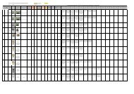
Nr.<br />
No.<br />
Manufacturer<br />
Hersteller<br />
G02. EU-St<strong>and</strong>ard<br />
H01.<br />
H)<br />
Thickness<br />
I)<br />
I01. VLSI<br />
Inst. Mikro<br />
elektroden<br />
Roughness<br />
Modell<br />
Model<br />
partly available<br />
from<br />
Nanosensors<br />
H)<br />
Schichtdicke<br />
SiO2 on Si<br />
I)<br />
Rauheit<br />
RAS-90, 220,<br />
440, 900, 2250,<br />
4700<br />
Measureme<br />
nt range<br />
Messbereich<br />
Description<br />
Beschreibung<br />
I<br />
M<br />
A<br />
G<br />
E<br />
Lateral<br />
Measure<br />
ment<br />
Range<br />
lateraler<br />
Messbere<br />
ich<br />
(nm) (μm)<br />
Material<br />
Material<br />
Substrat<br />
Substrate<br />
Dimension<br />
Dimension.<br />
(mm)<br />
Coating<br />
Beschichtung<br />
Material<br />
Material<br />
PV < 10 Flat ref. area I ≤ 250 x 250 Quartz 5 x 7 x 2 Cr 100<br />
7, 20, 70, 300,<br />
800<br />
9, 22, 44, 90,<br />
225, 470<br />
3 lines with different<br />
width 5, 30, <strong>and</strong> 100 µm<br />
4 separate fields with 6,<br />
20, 60, <strong>and</strong> 200 µm pitch<br />
rectangular profile<br />
Home<br />
Home<br />
Home<br />
I ≤ 4000 SiO2/Si 5 x 7 Cr 100<br />
I<br />
≤ ~5000 x<br />
4500<br />
Silicon<br />
die on<br />
Quartz<br />
25 x 25 x 6<br />
Thickne<br />
ss<br />
Dicke<br />
(nm)<br />
Remarks<br />
Bemerkungen<br />
Roughness st<strong>and</strong>ard<br />
<strong>for</strong> Ra