

CD4069UBC Inverter Circuits - Fairchild Semiconductor
CD4069UBC Inverter Circuits - Fairchild Semiconductor
CD4069UBC Inverter Circuits - Fairchild Semiconductor

You also want an ePaper? Increase the reach of your titles
YUMPU automatically turns print PDFs into web optimized ePapers that Google loves.
<strong>CD4069UBC</strong><br />
<strong>Inverter</strong> <strong>Circuits</strong><br />
General Description<br />
The CD4069UB consists of six inverter circuits and is manufactured<br />
using complementary MOS (CMOS) to achieve<br />
wide power supply operating range, low power consumption,<br />
high noise immunity, and symmetric controlled rise<br />
and fall times.<br />
This device is intended for all general purpose inverter<br />
applications where the special characteristics of the<br />
MM74C901, MM74C907, and CD4049A Hex <strong>Inverter</strong>/Buffers<br />
are not required. In those applications requiring larger<br />
noise immunity the MM74C14 or MM74C914 Hex Schmitt<br />
Trigger is suggested.<br />
All inputs are protected from damage due to static discharge<br />
by diode clamps to VDD and VSS. Ordering Code:<br />
Features<br />
Device also available in Tape and Reel. Specify by appending suffix “X” to the ordering code.<br />
October 1987<br />
Revised April 2002<br />
■ Wide supply voltage range: 3.0V to 15V<br />
■ High noise immunity: 0.45 VDD typ.<br />
■ Low power TTL compatibility: Fan out of 2 driving 74L<br />
or 1 driving 74LS<br />
■ Equivalent to MM74C04<br />
Order Number Package Number Package Description<br />
<strong>CD4069UBC</strong>M M14A 14-Lead Small Outline Integrated Circuit (SOIC), JEDEC MS-012, 0.150" Narrow<br />
<strong>CD4069UBC</strong>SJ M14D 14-Lead Small Outline Package (SOP), EIAJ TYPE II, 5.3mm Wide<br />
<strong>CD4069UBC</strong>N N14A 14-Lead Plastic Dual-In-Line Package (PDIP), JEDEC MS-001, 0.300" Wide<br />
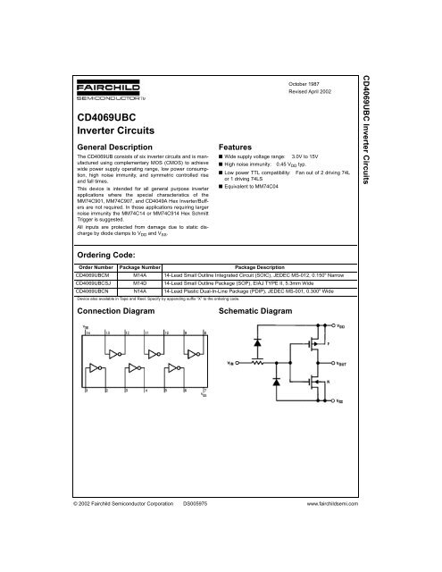
Connection Diagram Schematic Diagram<br />
© 2002 <strong>Fairchild</strong> <strong>Semiconductor</strong> Corporation DS005975 www.fairchildsemi.com<br />
<strong>CD4069UBC</strong> <strong>Inverter</strong> <strong>Circuits</strong>
<strong>CD4069UBC</strong><br />
Absolute Maximum Ratings(Note 1)<br />
(Note 2)<br />
DC Supply Voltage (V DD) −0.5V to +18 V DC<br />
Input Voltage (V IN ) −0.5V to V DD +0.5 V DC<br />
Storage Temperature Range (T S ) −65°C to +150°C<br />
Power Dissipation (PD) Dual-In-Line 700 mW<br />
Small Outline 500 mW<br />
Lead Temperature (TL) (Soldering, 10 seconds) 260°C<br />
DC Electrical Characteristics (Note 3)<br />
Note 3: VSS = 0V unless otherwise specified.<br />
Note 4: IOH and IOL are tested one output at a time.<br />
www.fairchildsemi.com 2<br />
Recommended Operating<br />
Conditions (Note 2)<br />
DC Supply Voltage (V DD ) 3V to 15V DC<br />
Input Voltage (V IN ) 0V to V DD V DC<br />
Operating Temperature Range (T A) −55°C to +125°C<br />
Note 1: “Absolute Maximum Ratings” are those values beyond which the<br />
safety of the device cannot be guaranteed. They are not meant to imply<br />
that the devices should be operated at these limits. The table of “Recommended<br />
Operating Conditions” and Electrical Characteristics table provide<br />
conditions for actual device operation.<br />
Note 2: VSS = 0V unless otherwise specified.<br />
Symbol Parameter Conditions<br />
−55°C<br />
Min Max Min<br />
+25°C<br />
Typ Max<br />
+125°C<br />
Min Max<br />
IDD Quiescent Device Current VDD = 5V, 0.25 0.25 7.5<br />
VIN = VDD or VSS VDD = 10V,<br />
VIN = VDD or VSS 0.5 0.5 15<br />
VDD = 15V,<br />
VIN = VDD or VSS 1.0 1.0 30<br />
VOL LOW Level Output Voltage |IO| < 1 µA<br />
VDD = 5V 0.05 0 0.05 0.05<br />
VDD = 10V 0.05 0 0.05 0.05<br />
VDD = 15V 0.05 0 0.05 0.05<br />
VOH HIGH Level Output Voltage |IO | < 1 µA<br />
VDD = 5V 4.95 4.95 5 4.95<br />
VDD = 10V 9.95 9.95 10 9.95<br />
VDD = 15V 14.95 14.95 15 14.95<br />
VIL LOW Level Input Voltage |IO| < 1 µA<br />
VDD = 5V, VO = 4.5V 1.0 1.0 1.0<br />
VDD = 10V, VO = 9V 2.0 2.0 2.0<br />
VDD = 15V, VO = 13.5V 3.0 3.0 3.0<br />
VIH HIGH Level Input Voltage |IO| < 1 µA<br />
VDD = 5V, VO = 0.5V 4.0 4.0 4.0<br />
VDD = 10V, VO = 1V 8.0 8.0 8.0<br />
VDD = 15V, VO = 1.5V 12.0 12.0 12.0<br />
IOL LOW Level Output Current VDD = 5V, VO = 0.4V 0.64 0.51 0.88 0.36<br />
(Note 4) VDD = 10V, VO = 0.5V 1.6 1.3 2.25 0.9<br />
VDD = 15V, VO = 1.5V 4.2 3.4 8.8 2.4<br />
IOH HIGH Level Output Current VDD = 5V, VO = 4.6V −0.64 −0.51 −0.88 −0.36<br />
(Note 4) VDD = 10V, VO = 9.5V −1.6 −1.3 −2.25 −0.9<br />
VDD = 15V, VO = 13.5V −4.2 −3.4 −8.8 −2.4<br />
IIN Input Current VDD = 15V, VIN = 0V −0.1 −10−5 −0.1 −1.0<br />
V DD = 15V, V IN = 15V 0.1 10 −5<br />
0.1 1.0<br />
Units<br />
µA<br />
V<br />
V<br />
V<br />
V<br />
mA<br />
mA<br />
µA
AC Electrical Characteristics (Note 5)<br />
TA = 25°C, CL = 50 pF, RL = 200 kΩ, tr and tf ≤ 20 ns, unless otherwise specified<br />
Symbol Parameter Conditions Min Typ Max Units<br />
tPHL or tPLH Propagation Delay Time from VDD = 5V 50 90<br />
Input to Output VDD = 10V 30 60<br />
ns<br />
VDD = 15V 25 50<br />
tTHL or tTLH Transition Time VDD = 5V 80 150<br />
VDD = 10V 50 100 ns<br />
VDD = 15V 40 80<br />
CIN Average Input Capacitance Any Gate 6 15 pF<br />
CPD Power Dissipation Capacitance Any Gate (Note 6) 12 pF<br />
Note 5: AC Parameters are guaranteed by DC correlated testing.<br />
Note 6: CPD determines the no load AC power consumption of any CMOS device. For complete explanation, see Family Characteristics application note—<br />
AN-90.<br />
AC Test <strong>Circuits</strong> and Switching Time Waveforms<br />
3 www.fairchildsemi.com<br />
<strong>CD4069UBC</strong>
<strong>CD4069UBC</strong><br />
Typical Performance Characteristics<br />
Gate Transfer Characteristics<br />
Power Dissipation vs. Frequency<br />
Propagation Delay Time vs. Load Capacitance<br />
www.fairchildsemi.com 4<br />
Propagation Delay vs. Ambient Temperature<br />
Propagation Delay vs. Ambient Temperature
Physical Dimensions inches (millimeters) unless otherwise noted<br />
14-Lead Small Outline Integrated Circuit (SOIC), JEDEC MS-012, 0.150" Narrow<br />
Package Number M14A<br />
5 www.fairchildsemi.com<br />
<strong>CD4069UBC</strong>
<strong>CD4069UBC</strong><br />
Physical Dimensions inches (millimeters) unless otherwise noted (Continued)<br />
14-Lead Small Outline Package (SOP), EIAJ TYPE II, 5.3mm Wide<br />
Package Number M14D<br />
www.fairchildsemi.com 6
Physical Dimensions inches (millimeters) unless otherwise noted (Continued)<br />
14-Lead Plastic Dual-In-Line Package (PDIP), JEDEC MS-001, 0.300" Wide<br />
Package Number N14A<br />
<strong>Fairchild</strong> does not assume any responsibility for use of any circuitry described, no circuit patent licenses are implied and<br />
<strong>Fairchild</strong> reserves the right at any time without notice to change said circuitry and specifications.<br />
LIFE SUPPORT POLICY<br />
FAIRCHILD’S PRODUCTS ARE NOT AUTHORIZED FOR USE AS CRITICAL COMPONENTS IN LIFE SUPPORT<br />
DEVICES OR SYSTEMS WITHOUT THE EXPRESS WRITTEN APPROVAL OF THE PRESIDENT OF FAIRCHILD<br />
SEMICONDUCTOR CORPORATION. As used herein:<br />
1. Life support devices or systems are devices or systems<br />
which, (a) are intended for surgical implant into the<br />
body, or (b) support or sustain life, and (c) whose failure<br />
to perform when properly used in accordance with<br />
instructions for use provided in the labeling, can be reasonably<br />
expected to result in a significant injury to the<br />
user.<br />
2. A critical component in any component of a life support<br />
device or system whose failure to perform can be reasonably<br />
expected to cause the failure of the life support<br />
device or system, or to affect its safety or effectiveness.<br />
www.fairchildsemi.com<br />
7 www.fairchildsemi.com<br />
<strong>CD4069UBC</strong> <strong>Inverter</strong> <strong>Circuits</strong>


