

Half-Bridge LLC Resonant Converter Design Using FSFR-Series ...
Half-Bridge LLC Resonant Converter Design Using FSFR-Series ...
Half-Bridge LLC Resonant Converter Design Using FSFR-Series ...

Create successful ePaper yourself
Turn your PDF publications into a flip-book with our unique Google optimized e-Paper software.
AN-4151<br />
www.fairchildsemi.com<br />
<strong>Half</strong>-<strong>Bridge</strong> <strong>LLC</strong> <strong>Resonant</strong> <strong>Converter</strong> <strong>Design</strong> <strong>Using</strong><br />
<strong>FSFR</strong>-<strong>Series</strong> Fairchild Power Switch (FPS)<br />
Introduction<br />
The effort to obtain ever-increasing power density of<br />
switched-mode power supply has been limited by the size<br />
of passive components. Operation at higher frequencies<br />
considerably reduces the size of passive components, such<br />
as transformers and filters; however, switching losses have<br />
been an obstacle to high-frequency operation. To reduce<br />
switching losses and allow high-frequency operation,<br />
resonant switching techniques have been developed.<br />
These techniques process power in a sinusoidal manner<br />
and the switching devices are softly commutated.<br />
Therefore, the switching losses and noise can be<br />
dramatically reduced [1-7].<br />
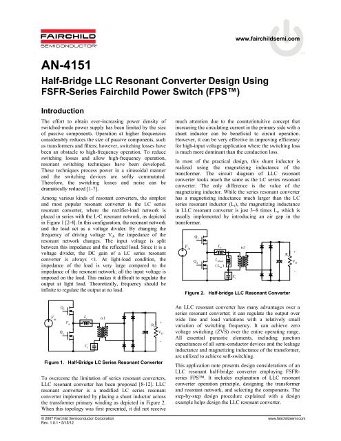
Among various kinds of resonant converters, the simplest<br />
and most popular resonant converter is the LC series<br />
resonant converter, where the rectifier-load network is<br />
placed in series with the L-C resonant network, as depicted<br />
in Figure 1 [2-4]. In this configuration, the resonant network<br />
and the load act as a voltage divider. By changing the<br />
frequency of driving voltage Vd, the impedance of the<br />
resonant network changes. The input voltage is split<br />
between this impedance and the reflected load. Since it is a<br />
voltage divider, the DC gain of a LC series resonant<br />
converter is always
AN-4151 APPLICATION NOTE<br />
1. <strong>LLC</strong> <strong>Resonant</strong> <strong>Converter</strong> and<br />
Fundamental Approximation<br />
Figure 3 shows the simplified schematic of a half-bridge<br />
<strong>LLC</strong> resonant converter, where Lm is the magnetizing<br />
inductance that acts as a shunt inductor, Lr is the series<br />
resonant inductor, and Cr is the resonant capacitor.<br />
Figure 4 illustrates the typical waveforms of the <strong>LLC</strong><br />
resonant converter. It is assumed that the operation<br />
frequency is same as the resonance frequency, determined<br />
by the resonance between Lr and Cr. Since the magnetizing<br />
inductor is relatively small, there exists considerable<br />
amount of magnetizing current (Im), which freewheels in<br />
the primary side without being involved in the power<br />
transfer. The primary-side current (Ip) is sum of the<br />
magnetizing current and the secondary-side current<br />
referred to the primary.<br />
In general, the <strong>LLC</strong> resonant topology consists of three<br />
stages shown in Figure 3; square wave generator, resonant<br />
network, and rectifier network.<br />
The square wave generator produces a square wave<br />
voltage, Vd, by driving switches Q1 and Q2 alternately<br />
with 50% duty cycle for each switch. A small dead<br />
time is usually introduced between the consecutive<br />
transitions. The square wave generator stage can be<br />
built as a full-bridge or half-bridge type.<br />
The resonant network consists of a capacitor, leakage<br />
inductances, and the magnetizing inductance of the<br />
transformer. The resonant network filters the higher<br />
harmonic currents. Essentially, only sinusoidal current<br />
is allowed to flow through the resonant network even<br />
though a square wave voltage is applied to the<br />
resonant network. The current (Ip) lags the voltage<br />
applied to the resonant network (that is, the<br />
fundamental component of the square wave voltage<br />
(Vd) applied to the half-bridge totem pole), which<br />
allows the MOSFETs to be turned on with zero<br />
voltage. As shown in Figure 4, the MOSFET turns on<br />
while the voltage across the MOSFET is zero by<br />
flowing current through the anti-parallel diode.<br />
The rectifier network produces DC voltage by<br />
rectifying the AC current with rectifier diodes and<br />
capacitor. The rectifier network can be implemented<br />
as a full-wave bridge or center-tapped configuration<br />
with capacitive output filter.<br />
Square wave generator<br />
V in<br />
Q 2<br />
Q 1<br />
I DS1<br />
+<br />
V d<br />
-<br />
resonant network Rectifier network<br />
C r<br />
L r<br />
I m<br />
L m<br />
I p<br />
n:1<br />
Figure 3. Schematic of <strong>Half</strong>-bridge <strong>LLC</strong><br />
<strong>Resonant</strong> <strong>Converter</strong><br />
I D<br />
R o<br />
I o<br />
+<br />
V O<br />
-<br />
© 2007 Fairchild Semiconductor Corporation www.fairchildsemi.com<br />
Rev. 1.0.1 • 5/15/12 2<br />
I DS1<br />
I D<br />
V d<br />
V gs1<br />
V gs2<br />
I p<br />
I m<br />
V in<br />
Figure 4. Typical Waveforms of <strong>Half</strong>-bridge <strong>LLC</strong><br />
<strong>Resonant</strong> <strong>Converter</strong><br />
The filtering action of the resonant network allows use of<br />
the fundamental approximation to obtain the voltage gain<br />
of the resonant converter, which assumes that only the<br />
fundamental component of the square-wave voltage input<br />
to the resonant network contributes to the power transfer to<br />
the output. Because the rectifier circuit in the secondary<br />
side acts as an impedance transformer, the equivalent load<br />
resistance is different from actual load resistance. Figure 5<br />
shows how this equivalent load resistance is derived. The<br />
primary-side circuit is replaced by a sinusoidal current<br />
source, Iac, and a square wave of voltage, VRI, appears at<br />
the input to the rectifier. Since the average of |Iac| is the<br />
output current, Io, Iac, is obtained as:<br />
Io<br />
Iac sin( t)<br />
2<br />
and VRI is given as:<br />
(1)<br />
VRI Vo V V if sin( t)<br />
0<br />
if sin( t)<br />
0<br />
(2)<br />
RI o<br />
where Vo is the output voltage.<br />
The fundamental component of VRI is given as:<br />
F 4Vo<br />
VRI sin( t)<br />
(3)<br />
<br />
Since harmonic components of VRI are not involved in the<br />
power transfer, AC equivalent load resistance can be<br />
calculated by dividing VRI F by Iac as:<br />
Rac F<br />
VRI<br />
Iac 8 Vo<br />
2<br />
Io<br />
8<br />
R 2 o<br />
<br />
(4)<br />
Considering the transformer turns ratio (n=Np/Ns), the<br />
equivalent load resistance shown in the primary side is<br />
obtained as:<br />
2<br />
8n<br />
R R<br />
(5)<br />
ac 2 o
AN-4151 APPLICATION NOTE<br />
By using the equivalent load resistance, the AC equivalent<br />
circuit is obtained, as illustrated in Figure 6, where Vd F and<br />
VRO F are the fundamental components of the driving voltage,<br />
Vd and reflected output voltage, VRO (nVRI), respectively.<br />
I ac<br />
I ac<br />
F VRI V RI<br />
+<br />
V RI<br />
-<br />
pk<br />
I ac<br />
V o<br />
I<br />
ac<br />
R o<br />
I o<br />
+<br />
V O<br />
F 4Vo<br />
VRI sin( wt)<br />
<br />
-<br />
Io<br />
sin( wt)<br />
2<br />
<br />
Figure 5. Derivation of Equivalent Load Resistance Rac<br />
V in<br />
V d<br />
+<br />
n=N p /N s<br />
-<br />
F Vd C r<br />
C r<br />
L r<br />
L m<br />
8n<br />
R R<br />
<br />
ac <br />
2<br />
2 o<br />
L r<br />
Lm<br />
N p :N s<br />
+<br />
V RI<br />
-<br />
R ac<br />
+<br />
VO R o<br />
-<br />
F VRo (nV RI F )<br />
Figure 6. AC Equivalent Circuit for <strong>LLC</strong> <strong>Resonant</strong><br />
<strong>Converter</strong><br />
With the equivalent load resistance obtained in Equation 5,<br />
the characteristics of the <strong>LLC</strong> resonant converter can be<br />
derived. <strong>Using</strong> the AC equivalent circuit of Figure 6, the<br />
voltage gain, M, is obtained as:<br />
4nV<br />
o<br />
F F sin( t)<br />
VRO nVRI 2n<br />
Vo<br />
M<br />
<br />
<br />
<br />
F F<br />
V 4<br />
d V V<br />
d in sin( t)<br />
Vin<br />
2<br />
(6)<br />
2<br />
( ) ( m 1)<br />
o<br />
2 2<br />
<br />
( 1) j ( 1)( m1) Q<br />
2 2<br />
<br />
p o o<br />
where:<br />
2<br />
8n<br />
Lp<br />
Lp Lm Lr , Rac R , 2 o m Lr<br />
Lr<br />
1 1 1<br />
Q , o , p<br />
<br />
C R LC LC<br />
r ac r r p r<br />
As can be seen in Equation 6, there are two resonant<br />
frequencies. One is determined by Lr and Cr, while the<br />
other is determined by Lp and Cr.<br />
Equation 6 shows the gain is unity at resonant frequency<br />
(ωo), regardless of the load variation, which is given as:<br />
2<br />
2nV<br />
( m 1) <br />
o<br />
p<br />
M 1at(7) 2 2<br />
o<br />
V <br />
in o p<br />
The gain of Equation 6 is plotted in Figure 7 for different<br />
Q values with m=3, fo=100kHz, and fp=57kHz. As<br />
observed in Figure 7, the <strong>LLC</strong> resonant converter shows<br />
gain characteristics that are almost independent of the load<br />
when the switching frequency is around the resonant<br />
frequency, fo. This is a distinct advantage of <strong>LLC</strong>-type<br />
resonant converter over the conventional series resonant<br />
converter. Therefore, it is natural to operate the converter<br />
around the resonant frequency to minimize the switching<br />
frequency variation.<br />
The operating range of the <strong>LLC</strong> resonant converter is<br />
limited by the peak gain (attainable maximum gain), which<br />
is indicated with ‘*’ in Figure 7. It should be noted that the<br />
peak voltage gain does not occur at fo nor fp. The peak gain<br />
frequency where the peak gain is obtained exists between<br />
fp and fo, as shown in Figure 7. As Q decreases (as load<br />
decreases), the peak gain frequency moves to fp and higher<br />
peak gain is obtained. Meanwhile, as Q increases (as load<br />
increases), the peak gain frequency moves to fo and the<br />
peak gain drops; thus, the full load condition should be the<br />
worst case for the resonant network design.<br />
0.6<br />
40 50 60 70 80 90<br />
freq (kHz)<br />
100 110 120 130 140<br />
© 2007 Fairchild Semiconductor Corporation www.fairchildsemi.com<br />
Rev. 1.0.1 • 5/15/12 3<br />
Gain ( 2nV o / V in )<br />
2.0<br />
1.8<br />
1.6<br />
1.4<br />
1.2<br />
1.0<br />
0.8<br />
1<br />
f p <br />
2<br />
L C<br />
Q=0.25<br />
p r<br />
Q=1.0<br />
M 1<br />
@ fo<br />
1<br />
fo<br />
<br />
2<br />
LrCr Q <br />
L / C<br />
r r<br />
Rac<br />
Q=1.0<br />
Q=0.75<br />
Q=0.50<br />
Q=0.25<br />
Figure 7. Typical Gain Curves of <strong>LLC</strong> <strong>Resonant</strong><br />
<strong>Converter</strong> (m=3)
AN-4151 APPLICATION NOTE<br />
2. Consideration for Integrated<br />
Transformer<br />
For practical design, it is common to implement the<br />
magnetic components (series inductor and shunt inductor)<br />
using an integrated transformer; where the leakage<br />
inductance is used as a series inductor, while the<br />
magnetizing inductor is used as a shunt inductor. When<br />
building the magnetizing components in this way, the<br />
equivalent circuit in Figure 6 should be modified as shown<br />
in Figure 8 because the leakage inductance exists, not only<br />
in the primary side, but also in the secondary side. Not<br />
considering the leakage inductance in the transformer<br />
secondary side generally results in an incorrect design.<br />
V in<br />
+<br />
V F<br />
in<br />
V d<br />
+<br />
-<br />
Cr<br />
C r<br />
L L L n L<br />
Llkp Lm//<br />
Llkp<br />
L L L<br />
L r<br />
L lkp<br />
L p -L r<br />
L m<br />
2<br />
r lkp m //( lks )<br />
p lkp m<br />
-<br />
n:1<br />
1: V M<br />
L lks<br />
+<br />
V RI<br />
-<br />
Lp<br />
( MV<br />
)<br />
L L<br />
ideal<br />
transformer<br />
Rac<br />
p r<br />
+<br />
VO R o<br />
-<br />
+<br />
V F<br />
RO<br />
F (nV ) RI<br />
-<br />
Figure 8. Modified Equivalent Circuit to Accommodate<br />
the Secondary-side Leakage Inductance<br />
In Figure 8, the effective series inductor (Lp) and shunt<br />
inductor (Lp-Lr) are obtained by assuming n 2 Llks=Llkp and<br />
referring the secondary-side leakage inductance to the<br />
primary side as:<br />
L L L<br />
p m lkp<br />
r lkp m //(<br />
2<br />
lks) lkp m // lkp<br />
L L L n L L L L<br />
When handling an actual transformer, equivalent circuit<br />
with Lp and Lr is preferred since these values can be easily<br />
measured with a given transformer. In an actual<br />
transformer, Lp and Lr can be measured in the primary side<br />
with the secondary-side winding open circuited and short<br />
circuited, respectively.<br />
In Figure 9, notice that a virtual gain MV is introduced,<br />
which is caused by the secondary-side leakage inductance.<br />
By adjusting the gain equation of Equation 6 using the<br />
modified equivalent circuit of Figure 9, the gain equation<br />
for integrated transformer is obtained:<br />
(8)<br />
<br />
m MV<br />
2nV<br />
M <br />
V<br />
( 1) j( ) ( 1) ( m1) Q<br />
O<br />
2<br />
( )<br />
o<br />
( 1)<br />
in<br />
2<br />
<br />
2<br />
<br />
2<br />
p o 2<br />
o<br />
<br />
( ) mm ( 1)<br />
<br />
<br />
(<br />
<br />
<br />
1) j( ) ( <br />
1) ( m1) Q<br />
2<br />
2<br />
o<br />
2 2<br />
2 2<br />
p o o<br />
2<br />
e 8n<br />
Ro Lp<br />
Rac , m<br />
2 2<br />
where: MV Lr<br />
e<br />
Q <br />
Lr<br />
C<br />
1<br />
, e o <br />
R<br />
1<br />
LC<br />
, p<br />
<br />
1<br />
LC<br />
r ac r r p r<br />
The gain at the resonant frequency (ωo) is fixed regardless<br />
of the load variation, which is given as:<br />
Lp m<br />
M MV ato<br />
L L m1<br />
© 2007 Fairchild Semiconductor Corporation www.fairchildsemi.com<br />
Rev. 1.0.1 • 5/15/12 4<br />
p r<br />
e<br />
e<br />
(9)<br />
(10)<br />
The gain at the resonant frequency (ωo) is unity when<br />
using individual core for series inductor, as shown in<br />
Equation 7. However, when implementing the magnetic<br />
components with integrated transformer, the gain at the<br />
resonant frequency (ωo) is larger than unity due to the<br />
virtual gain caused by the leakage inductance in the<br />
transformer secondary side.<br />
The gain of Equation 9 is plotted in Figure 10 for different<br />
Q e values with m=3, fo=100kHz, and fp=57kHz. As observed<br />
in Figure 9, the <strong>LLC</strong> resonant converter shows gain<br />
characteristics almost independent of the load when the<br />
switching frequency is around the resonant frequency, fo.<br />
Gain ( 2nV o / V in )<br />
Qe 2.2<br />
=0.25<br />
2.0<br />
1.8<br />
1.6<br />
1.4<br />
1.2<br />
1.0<br />
1<br />
f p <br />
2<br />
L C<br />
p r<br />
Q e =1.0<br />
M M<br />
1<br />
fo<br />
<br />
2<br />
LrCr @ fo V<br />
e<br />
Q <br />
Lr / Cr<br />
e<br />
Rac<br />
Q e =1.00<br />
Q e =0.75<br />
Q e =0.50<br />
Q e =0.25<br />
0.8<br />
40 50 60 70 80 90<br />
freq (kHz)<br />
100 110 120 130 140<br />
Figure 9. Typical Gain Curves of <strong>LLC</strong> <strong>Resonant</strong><br />
<strong>Converter</strong> (m=3) <strong>Using</strong> an Integrated Transformer
AN-4151 APPLICATION NOTE<br />
3. Consideration of Operation Mode<br />
and Attainable Maximum Gain<br />
Operation Mode<br />
The <strong>LLC</strong> resonant converter can operate at frequency<br />
below or above the resonance frequency (fo), as<br />
illustrated in Figure 10. Figure 11 shows the waveforms<br />
of the currents in the transformer primary side and<br />
secondary side for each operation mode. Operation<br />
below the resonant frequency (case I) allows the soft<br />
commutation of the rectifier diodes in the secondary<br />
side, while the circulating current is relatively large. The<br />
circulating current increases more as the operation<br />
frequency moves downward from the resonant<br />
frequency. Meanwhile, operation above the resonant<br />
frequency (case II) allows the circulating current to be<br />
minimized, but the rectifier diodes are not softly<br />
commutated. Below resonance operation is preferred for<br />
high output voltage applications, such as Plasma Display<br />
Panel (PDP) TV where the reverse recovery loss in the<br />
rectifier diode is severe. Below resonance operation also<br />
has a narrow frequency range with respect to the load<br />
variation since the frequency is limited below the<br />
resonance frequency even at no load condition.<br />
On the other hand, above resonance operation has less<br />
conduction loss than the below resonance operation. It can<br />
show better efficiency for low output voltage applications,<br />
such as Liquid Crystal Display (LCD) TV or laptop<br />
adaptor, where Schottky diodes are available for the<br />
secondary-side rectifiers and reverse recovery problems<br />
are insignificant. However, operation at above the resonant<br />
frequency may cause too much frequency increase at lightload<br />
condition. Above frequency operation requires<br />
frequency skipping to prevent too much increase of the<br />
switching frequency.<br />
Gain (M)<br />
B<br />
A<br />
I<br />
Below resonance<br />
(f s f o )<br />
Figure 10. Operation Modes According to the Operation<br />
Frequency<br />
f s<br />
© 2007 Fairchild Semiconductor Corporation www.fairchildsemi.com<br />
Rev. 1.0.1 • 5/15/12 5<br />
I p<br />
I DS1<br />
ID<br />
I p<br />
I DS1<br />
I m<br />
I m<br />
1<br />
2 fo<br />
1<br />
2 fS<br />
(I) f s < f o<br />
I D I O<br />
I O<br />
(II) f s > f o<br />
Figure 11. Waveforms of Each Operation Mode<br />
Required Maximum Gain and Peak Gain<br />
Above the peak gain frequency, the input impedance of<br />
the resonant network is inductive and the input current of<br />
the resonant network (Ip) lags the voltage applied to the<br />
resonant network (Vd). This permits the MOSFETs to<br />
turn on with zero voltage (ZVS), as illustrated in Figure<br />
12. Meanwhile, the input impedance of the resonant<br />
network becomes capacitive and Ip leads Vd below the<br />
peak gain frequency. When operating in capacitive<br />
region, the MOSFET body diode is reverse recovered<br />
during the switching transition, which results in severe<br />
noise. Another problem of entering into the capacitive<br />
region is that the output voltage becomes out of control<br />
since the slope of the gain is reversed. The minimum<br />
switching frequency should be well limited above the<br />
peak gain frequency.<br />
V d<br />
I p<br />
I DS1<br />
M<br />
capacitive<br />
region<br />
peak gain<br />
V d<br />
I p<br />
I DS1<br />
inductive<br />
region<br />
reverse recovery ZVS<br />
Figure 12. Operation Waveforms for Capacitive and<br />
Inductive Regions<br />
f s
AN-4151 APPLICATION NOTE<br />
The available input voltage range of the <strong>LLC</strong> resonant<br />
converter is determined by the peak voltage gain. Thus, the<br />
resonant network should be designed so that the gain curve<br />
has an enough peak gain to cover the input voltage range.<br />
However, ZVS condition is lost below the peak gain point,<br />
as depicted in Figure 12. Therefore, some margin is required<br />
when determining the maximum gain to guarantee stable<br />
ZVS operation during the load transient and start-up.<br />
Typically 10~20% of the maximum gain is used as a margin<br />
for practical design, as shown in Figure 13.<br />
Gain (M)<br />
10~20% of M max<br />
peak gain<br />
maximum operation gain<br />
(M max )<br />
fo Figure 13. Determining the Maximum Gain<br />
Even though the peak gain at a given condition can be<br />
obtained by using the gain in Equation 6, it is difficult to<br />
express the peak gain in explicit form. To simplify the<br />
analysis and design, the peak gains are obtained using<br />
simulation tools and depicted in Figure 14, which shows<br />
how the peak gain (attainable maximum gain) varies with<br />
Q for different m values. It appears that higher peak gain<br />
can be obtained by reducing m or Q values. With a given<br />
resonant frequency (fo) and Q value, decreasing m means<br />
reducing the magnetizing inductance, which results in<br />
increased circulating current. Accordingly, there is a tradeoff<br />
between the available gain range and conduction loss.<br />
f s<br />
1<br />
0.2 0.3 0.4 0.5 0.6 0.7 0.8 0.9 1 1.1 1.2 1.3 1.4<br />
© 2007 Fairchild Semiconductor Corporation www.fairchildsemi.com<br />
Rev. 1.0.1 • 5/15/12 6<br />
peak gain<br />
2.2<br />
2.1<br />
2<br />
1.9<br />
1.8<br />
1.7<br />
1.6<br />
1.5<br />
1.4<br />
1.3<br />
1.2<br />
1.1<br />
m=3.0<br />
m=3.5<br />
m=4.0<br />
m=4.5<br />
m=5.0<br />
m=6.0<br />
m=9.0 m=8.0 m=7.0<br />
Q<br />
m=2.25<br />
m=2.5<br />
Figure 14. Peak Gain (Attainable Maximum Gain) vs.<br />
Q for Different m Values
AN-4151 APPLICATION NOTE<br />
4. Features of <strong>FSFR</strong>-<strong>Series</strong><br />
<strong>FSFR</strong>-series is an integrated Pulse Frequency Modulation<br />
(PFM) controller and MOSFETs specifically designed for<br />
Zero Voltage Switching (ZVS) half-bridge converters with<br />
minimal external components. The internal controller<br />
includes an under-voltage lockout, optimized high-side /<br />
low-side gate driver, temperature-compensated precise<br />
current controlled oscillator, and self-protection circuitry.<br />
Compared with discrete MOSFET and PWM controller<br />
solution, <strong>FSFR</strong>-series can reduce total cost, component<br />
count, size and weight, while simultaneously increasing<br />
efficiency, productivity, and system reliability.<br />
R T<br />
CON<br />
1 2 3 4 5 6 7 8 9 10<br />
R SG LVcc<br />
T<br />
CON CS PG HVcc<br />
V DL<br />
3<br />
2<br />
Figure 15. Package Diagram<br />
V REF<br />
I CTC<br />
5V<br />
OLP<br />
LVcc<br />
OVP<br />
23V<br />
+<br />
LVcc<br />
I delay<br />
-<br />
+<br />
-<br />
+<br />
-<br />
I CTC<br />
2I CTC<br />
2V<br />
-<br />
0.6V/0.4V<br />
+<br />
3V<br />
1V<br />
LVcc good<br />
+<br />
-<br />
+<br />
-<br />
V CTR<br />
S<br />
R<br />
S Q<br />
R -Q<br />
F/F<br />
Counter (1/4)<br />
Q<br />
-Q<br />
Auto-restart<br />
protection<br />
11.3 / 14.5 V<br />
Q<br />
-Q<br />
Table 1. Pin Description<br />
This pin is the drain of the high-side<br />
1 VDL MOSFET, typically connected to the input<br />
DC link voltage.<br />
This pin is for enable/disable and protection.<br />
When the voltage of this pin is above 0.6V,<br />
the IC operation is enabled. Meanwhile,<br />
2 CON when the voltage of this pin drops below<br />
0.4V, gate drive signals for both MOSFETs<br />
are disabled. When the voltage of this pin<br />
increases above 5V, protection is triggered.<br />
This pin is to program the switching<br />
3 RT<br />
frequency. Typically, opto-coupler and<br />
resistor are connected to this pin to regulate<br />
the output voltage.<br />
This pin is to sense the current flowing<br />
4 CS through the low-side MOSFET. Typically<br />
negative voltage is applied on this pin.<br />
5 SG This pin is the control ground.<br />
6 PG<br />
This pin is the power ground. This pin is<br />
connected to the source of the low-side<br />
MOSFET.<br />
7 LVcc<br />
This pin is the supply voltage of the control<br />
IC.<br />
8 NC No connection.<br />
9 HVcc<br />
This pin is the supply voltage of the highside<br />
drive circuit.<br />
This pin is the drain of the low-side<br />
MOSFET. Typically transformer is<br />
connected to this pin.<br />
10 VCTR<br />
VAOCP<br />
TSD<br />
High-Side<br />
Gate Drive<br />
Low-Side<br />
Gate Drive<br />
© 2007 Fairchild Semiconductor Corporation www.fairchildsemi.com<br />
Rev. 1.0.1 • 5/15/12 7<br />
S<br />
R<br />
Latch<br />
protection<br />
LVcc<br />
7<br />
+<br />
-<br />
Time<br />
Delay<br />
350ns<br />
Time<br />
Delay<br />
350ns<br />
delay<br />
1.5s LVcc good<br />
Internal<br />
Bias<br />
LVcc < 5V<br />
-<br />
+<br />
Vref<br />
Level-Shift<br />
Balancing<br />
delay<br />
Shutdown without delay<br />
50ns delay<br />
+<br />
-<br />
V OCP<br />
Figure 16. Functional Block Diagram of <strong>FSFR</strong>-series<br />
0.6V<br />
HVcc good<br />
0.9V<br />
-1<br />
8.7 / 9.2 V<br />
4<br />
-<br />
+<br />
CS<br />
VDL<br />
1<br />
9<br />
HVcc<br />
10 VCTR 8 NC<br />
6<br />
PG<br />
5 SG
AN-4151 APPLICATION NOTE<br />
Vin<br />
(From PFC<br />
output)<br />
C DL<br />
R max<br />
Vcc<br />
R min<br />
C B<br />
C LVcc<br />
R LPF<br />
R SS<br />
C SS<br />
RT<br />
CON<br />
CS<br />
C LPF<br />
R sense<br />
LVcc<br />
R damp<br />
Control<br />
IC<br />
D boot<br />
VDL<br />
SG PG<br />
© 2007 Fairchild Semiconductor Corporation www.fairchildsemi.com<br />
Rev. 1.0.1 • 5/15/12 8<br />
Cr<br />
HVcc<br />
C HVcc<br />
V CTR<br />
L lkp<br />
Lm<br />
L lks<br />
Np Ns<br />
Integrated<br />
transformer<br />
Ns<br />
L lks<br />
D1<br />
D2<br />
R bias<br />
KA431<br />
Figure 17. Reference Circuit for <strong>Design</strong> Example of <strong>LLC</strong> <strong>Resonant</strong> <strong>Half</strong>-bridge <strong>Converter</strong><br />
5. <strong>Design</strong> Procedure<br />
In this section, a design procedure is presented using the<br />
schematic in Figure 17 as a reference. An integrated<br />
transformer with center tap, secondary side is used and<br />
input is supplied from power factor correction (PFC) preregulator.<br />
A DC/DC converter with 192W/24V output has<br />
been selected as a design example. The design<br />
specifications are as follows:<br />
- Nominal input voltage: 400VDC (output of PFC stage)<br />
- Output: 24V/8A (192W)<br />
- Hold-up time requirement: 20ms (50Hz line freq.)<br />
- DC link capacitor of PFC output: 220µF<br />
[STEP-1] Define the system specifications<br />
As a first step, define the following specification.<br />
Estimated efficiency (Eff): The power conversion<br />
efficiency must be estimated to calculate the maximum<br />
input power with a given maximum output power. If no<br />
reference data is available, use Eff = 0.88~0.92 for lowvoltage<br />
output applications and Eff = 0.92~0.96 for highvoltage<br />
output applications. With the estimated efficiency,<br />
the maximum input power is given as:<br />
P<br />
P<br />
o<br />
(11)<br />
in<br />
E ff<br />
Input voltage range (Vin min and Vin max ): The maximum<br />
input voltage would be the nominal PFC output voltage as:<br />
V V<br />
(12)<br />
max<br />
in O. PFC<br />
Even though the input voltage is regulated as constant by<br />
PFC pre-regulator, it drops during the hold-up time. The<br />
minimum input voltage considering the hold-up time<br />
requirement is given as:<br />
2PinTHU DL<br />
C o<br />
R d<br />
C F<br />
R F<br />
Vo<br />
min 2<br />
Vin VO.<br />
PFC (13)<br />
C<br />
where VO.PFC is the nominal PFC output voltage, THU is a<br />
hold-up time, and CDL is the DC link bulk capacitor.<br />
(<strong>Design</strong> Example) Assuming the efficiency is 92%,<br />
P 192<br />
o<br />
P 209W<br />
in<br />
E 0.92<br />
ff<br />
max<br />
Vin VO. PFC 400V<br />
min 2 2PT<br />
in HU<br />
Vin VO.<br />
PFC <br />
CDL<br />
3<br />
2 2 209 20 10<br />
400 349V<br />
6<br />
220 10<br />
[STEP-2] Determine the Maximum and<br />
Minimum Voltage Gains of the <strong>Resonant</strong><br />
Network<br />
As discussed in the previous section, it is typical to operate<br />
the <strong>LLC</strong> resonant converter around the resonant frequency<br />
(fo) to minimize switching frequency variation. Since the<br />
input of the <strong>LLC</strong> resonant converter is supplied from PFC<br />
output voltage, the converter should be designed to operate<br />
at fo for the nominal PFC output voltage.<br />
As observed in Equation 10, the gain at fo is a function of<br />
m (m=Lp/Lr). The gain at fo is determined by choosing that<br />
value of m. While a higher peak gain can be obtained with<br />
a small m value, too small m value results in poor coupling
AN-4151 APPLICATION NOTE<br />
of the transformer and deteriorates the efficiency. It is<br />
typical to set m to be 3~7, which results in a voltage gain<br />
of 1.1~1.2 at the resonant frequency (fo).<br />
With the chosen m value, the voltage gain for the nominal<br />
PFC output voltage is obtained as:<br />
M<br />
min<br />
<br />
m<br />
m 1<br />
@f=fo (14)<br />
which would be the minimum gain because the nominal<br />
PFC output voltage is the maximum input voltage (Vin max ).<br />
The maximum voltage gain is given as:<br />
max<br />
max Vin<br />
min<br />
M M min<br />
V<br />
(15)<br />
in<br />
(<strong>Design</strong> Example) The ratio (m) between Lp and Lr is<br />
chosen as 5. The minimum and maximum gains are<br />
obtained as:<br />
min VRO M max<br />
Vin <br />
2<br />
m<br />
<br />
m1<br />
5<br />
1.12<br />
51 max<br />
max Vin<br />
min 400<br />
M M 1.12 1.28<br />
min<br />
V 349<br />
M min<br />
in<br />
Gain (M)<br />
M max for Vin min<br />
1.28<br />
m<br />
MV<br />
1.12<br />
m 1<br />
Peak gain (available maximum gain)<br />
fo<br />
1.12<br />
for Vin max<br />
( VO.PFC )<br />
Figure 18. Maximum Gain / Minimum Gain<br />
[STEP-3] Determine the Transformer Turns<br />
Ratio (n=Np/Ns)<br />
With the minimum gain (M min ) obtained in STEP-2, the<br />
transformer turns ratio is given as:<br />
max<br />
N p Vin<br />
min<br />
n M<br />
(16)<br />
Ns 2( Vo VF)<br />
where VF is the secondary-side rectifier diode voltage<br />
drop.<br />
(<strong>Design</strong> Example) assuming VF is 0.9V,<br />
max<br />
N p Vin<br />
400<br />
n Mmin 1.12 9.00<br />
N 2( V V ) 2(24 0.9)<br />
s o F<br />
fs<br />
[STEP-4] Calculate the Equivalent Load<br />
Resistance<br />
With the transformer turns ratio obtained from Equation<br />
16, the equivalent load resistance is obtained as:<br />
2 2<br />
8n Vo<br />
Rac<br />
(17)<br />
2<br />
P<br />
(<strong>Design</strong> Example)<br />
2 2 2 2<br />
8n Vo<br />
89.0 24<br />
Rac<br />
197 2 2<br />
P 192<br />
© 2007 Fairchild Semiconductor Corporation www.fairchildsemi.com<br />
Rev. 1.0.1 • 5/15/12 9<br />
o<br />
[STEP-5] <strong>Design</strong> the <strong>Resonant</strong> Network<br />
With m value chosen in STEP-2, read proper Q value from<br />
the peak gain curves in Figure 14 that allows enough peak<br />
gain. Considering the load transient and stable zerovoltage-switching<br />
(ZVS) operation, 10~20% margin<br />
should be introduced on the maximum gain when<br />
determining the peak gain. Once the Q value is<br />
determined, the resonant parameters are obtained as:<br />
1<br />
Cr<br />
<br />
(18)<br />
2<br />
QfoRac 1<br />
Lr<br />
(19)<br />
2<br />
(2 fo) Cr<br />
Lp m L<br />
(20)<br />
r<br />
(<strong>Design</strong> Example)<br />
As calculated in STEP-2, the maximum voltage gain<br />
(M max ) for the minimum input voltage (Vin min ) is 1.28.<br />
With 15% margin, a peak gain of 1.47 is required. m<br />
has been chosen as 5 in STEP-2 and Q is obtained as<br />
0.4 from the peak gain curves in Figure 19. By<br />
selecting the resonant frequency as 100kHz, the<br />
resonant components are determined as:<br />
1 1<br />
Cr 20.2nF<br />
3<br />
2Q fo Rac 2 0.4 100 10 197<br />
1 1<br />
Lr 126H<br />
2 3 2 9<br />
(2 f ) C (2 10010 ) 20.210 o r<br />
L mL 630H<br />
peak gain<br />
p r<br />
1.7<br />
1.6<br />
1.5<br />
1.4<br />
1.3<br />
1.2<br />
1.1<br />
1<br />
0.2 0.3 0.4 0.5 0.6 0.7 0.8 0.9 1 1.1<br />
o<br />
m=4.0<br />
m=4.5<br />
m=5.0<br />
m=6.0<br />
m=9.0 m=8.0 m=7.0<br />
Q<br />
Figure 19. <strong>Resonant</strong> Network <strong>Design</strong> <strong>Using</strong> the Peak<br />
Gain (Attainable Maximum Gain)<br />
Curve for m=5
AN-4151 APPLICATION NOTE<br />
[STEP-6] <strong>Design</strong> the Transformer<br />
The worst case for the transformer design is the minimum<br />
switching frequency condition, which occurs at the<br />
minimum input voltage and full-load condition. To obtain<br />
the minimum switching frequency, plot the gain curve<br />
using gain Equation 9 and read the minimum switching<br />
frequency. The minimum number of turns for the<br />
transformer primary-side is obtained as:<br />
N<br />
min<br />
p<br />
nV ( V<br />
)<br />
<br />
2 f M B A<br />
o F<br />
min<br />
s V e<br />
(21)<br />
where Ae is the cross-sectional area of the transformer core<br />
in m 2 and B is the maximum flux density swing in Tesla,<br />
as shown in Figure 20. If there is no reference data, use<br />
B =0.3~0.4 T. Notice that a virtual gain MV is introduced,<br />
which is caused by the secondary-side leakage inductance<br />
(Refer to Figure 8).<br />
V RI<br />
B<br />
1/(2f s )<br />
n (V o +V F )/M V<br />
-n (V o +V F )/M V<br />
B<br />
Figure 20. Flux Density Swing<br />
Choose the proper number of turns for the secondary side<br />
that results in primary-side turns larger than Np min as:<br />
Np n Ns Np<br />
min<br />
(22)<br />
(<strong>Design</strong> Example) EER3542 core (Ae=107mm 2 ) is<br />
selected for the transformer. From the gain curve of<br />
Figure 21, the minimum switching frequency is<br />
obtained as 78kHz. The minimum primary-side turns<br />
of the transformer is given as<br />
min nV ( o VF)<br />
N p min<br />
2fs B1.12Ae 9.0 24.9<br />
30.4<br />
turns<br />
3 6<br />
277100.41.1210710 Choose Ns so that the resultant Np should be larger<br />
than Np min :<br />
N nN 19.09 N<br />
min<br />
p s p<br />
N nN 29.018 N<br />
min<br />
p s p<br />
N nN 39.027 N<br />
min<br />
p s p<br />
N nN 49.036 N<br />
min<br />
p s p<br />
Figure 21. Gain Curve<br />
[STEP-7] Transformer Construction<br />
Parameters Lp and Lr of the transformer were determined in<br />
STEP-5. Lp and Lr can be measured in the primary side<br />
with the secondary-side winding open circuited and short<br />
circuited, respectively. Since <strong>LLC</strong> converter design<br />
requires a relatively large Lr, a sectional bobbin is<br />
typically used, as shown in Figure 22, to obtain the desired<br />
Lr value. For a sectional bobbin, the number of turns and<br />
winding configuration are the major factors determining<br />
the value of Lr, while the gap length of the core does not<br />
affect Lr much. Lp can be easily controlled by adjusting the<br />
gap length. Table 2 shows measured Lp and Lr values with<br />
different gap lengths. A gap length of 0.10mm obtains<br />
values for Lp and Lr closest to the designed parameters.<br />
Np<br />
Figure 22. Sectional Bobbin<br />
Table 2. Measured Lp and Lr with Different Gap Lengths<br />
Gap length Lp Lr<br />
0.0mm 2,295μH 123μH<br />
0.05mm 943μH 122μH<br />
0.10mm 630μH 118μH<br />
0.15mm 488μH 117μH<br />
0.20mm 419μH 115μH<br />
0.25mm 366μH 114μH<br />
© 2007 Fairchild Semiconductor Corporation www.fairchildsemi.com<br />
Rev. 1.0.1 • 5/15/12 10<br />
N s2<br />
N s1
AN-4151 APPLICATION NOTE<br />
(<strong>Design</strong> Example)<br />
Final <strong>Resonant</strong> Network <strong>Design</strong><br />
Even though the integrated transformer approach in<br />
<strong>LLC</strong> resonant converter design can implement the<br />
magnetic components in a single core and save one<br />
magnetic component, the value of Lr is not easy to<br />
control in real transformer design. <strong>Resonant</strong> network<br />
design sometimes requires iteration with a resultant Lr<br />
value after the transformer is built. The resonant<br />
capacitor value is also changed since it should be<br />
selected among off-the-shelf capacitors. The final<br />
resonant network design is summarized in Table 3<br />
and the new gain curves are shown in Figure 23.<br />
Table 3. Final <strong>Resonant</strong> Network <strong>Design</strong> Parameters<br />
Parameters Initial design Final design<br />
Lp 630µH 630µH<br />
Lr 126H 118µH<br />
Cr 20nF 22nF<br />
fo 100kHz 99kHz<br />
m 5 5.34<br />
Q 0.4 0.36<br />
2.0<br />
1.8<br />
1.6<br />
1.4<br />
1.2<br />
1.0<br />
0.8<br />
M@fo 1.12 1.11<br />
Minimum freq 78kHz 72kHz<br />
f min normal f<br />
M max<br />
M min<br />
100% load<br />
80% load<br />
60% load<br />
40% load<br />
20% load<br />
0.6<br />
40 50 60 70 80 90<br />
freq (kHz)<br />
100 110 120 130 140<br />
Figure 23. Gain Curve of the Final <strong>Resonant</strong><br />
Network <strong>Design</strong><br />
[STEP-8] Select the <strong>Resonant</strong> Capacitor<br />
When choosing the resonant capacitor, the current rating<br />
should be considered because a considerable amount of<br />
current flows through the capacitor. The RMS current<br />
through the resonant capacitor is given as:<br />
I<br />
1 I n( V V<br />
)<br />
[ ] [<br />
] (23)<br />
RMS o 2 o F 2<br />
Cr<br />
E ff 2 2n 4 2 foMV( Lp Lr)<br />
The nominal voltage of the resonant capacitor in normal<br />
operation is given as:<br />
V 2 I<br />
max<br />
RMS<br />
nom<br />
C <br />
r<br />
in<br />
2<br />
Cr <br />
2<br />
foCr © 2007 Fairchild Semiconductor Corporation www.fairchildsemi.com<br />
Rev. 1.0.1 • 5/15/12 11<br />
V<br />
(24)<br />
However, the resonant capacitor voltage increases much<br />
higher than this at overload condition or load transient.<br />
Actual capacitor selection should be based on the Over-<br />
Current Protection (OCP) trip point. With the OCP level,<br />
IOCP, the maximum resonant capacitor voltage is obtained as:<br />
V<br />
max<br />
Cr<br />
V I<br />
<br />
<br />
max<br />
in OCP<br />
2<br />
min<br />
2 fS Cr<br />
(25)<br />
The minimum switching frequency is used in the equation<br />
because the frequency is typically forced to the minimum<br />
value by the feedback loop when output is overloaded.<br />
(<strong>Design</strong> Example)<br />
I<br />
1 I n( V V<br />
)<br />
[ ] [<br />
]<br />
RMS o 2 o F 2<br />
Cr<br />
E ff 2 2n 4 2 foMV( Lp Lr)<br />
1<br />
<br />
0.92<br />
1.32A<br />
8 [ ]<br />
2 2 9.0 9.0 (24 0.9)<br />
[<br />
4 2 99101.1151210 ]<br />
2 2<br />
3 6<br />
The peak current in the primary side in normal<br />
operation is:<br />
peak rms<br />
I 2I 1.86A<br />
Cr Cr<br />
OCP level is set to 3.0A with 50% margin on ICr peak :<br />
V<br />
V<br />
V 2 I<br />
max<br />
RMS<br />
nom<br />
C <br />
r<br />
in<br />
2<br />
Cr <br />
2<br />
fo Cr<br />
max<br />
Cr<br />
400 2 1.32<br />
3 9<br />
2 2 9910 2210 max<br />
Vin IOCP<br />
min<br />
2 2<br />
fS Cr<br />
336V<br />
400 3<br />
3 9<br />
2 2 7210 2210 502V<br />
630V rated low-ESR film capacitor is selected for the<br />
resonant capacitor.<br />
[STEP-9] Rectifier Network <strong>Design</strong><br />
When the center tap winding is used in the transformer<br />
secondary side, the diode voltage stress is twice the output<br />
voltage expressed as:<br />
V 2( V V )<br />
(26)<br />
D o F<br />
The RMS value of the current flowing through each<br />
rectifier diode is given as:
AN-4151 APPLICATION NOTE<br />
RMS <br />
ID I<br />
(27)<br />
o<br />
4<br />
Meanwhile, the ripple current flowing through output<br />
capacitor is given as:<br />
2<br />
RMS Io2 2 8<br />
Co ( ) o o<br />
I I I<br />
(28)<br />
2 2<br />
8<br />
The voltage ripple of the output capacitor is:<br />
<br />
Vo Io R<br />
(29)<br />
C<br />
2<br />
where RC is the effective series resistance (ESR) of the<br />
output capacitor and the power dissipation is the output<br />
capacitor is:<br />
P . ( I ) R<br />
(30)<br />
RMS 2<br />
Loss Co Co C<br />
(<strong>Design</strong> Example) The voltage stress and current<br />
stress of the rectifier diode are:<br />
VD 2( Vo VF) 2(240.9) 49.8<br />
RMS <br />
ID Io 6.28A<br />
4<br />
The 100V/20A Schottky diode is selected for the<br />
rectifier considering the voltage overshoot caused by<br />
the stray inductance.<br />
The RMS current of the output capacitor is:<br />
2<br />
RMS Io2 2 8<br />
ICo ( ) Io Io 3.857A<br />
2 2<br />
8<br />
When two electrolytic capacitors with ESR of 80mΩ<br />
are used in parallel, the output voltage ripple is given<br />
as:<br />
0.08<br />
Vo IoRC 8 ( ) 0.50V<br />
2 2 2<br />
The loss in electrolytic capacitors is:<br />
RMS 2 2<br />
PLoss. Co ( ICo) RC3.857 0.04 0.60W<br />
[STEP-10] Control Circuit Configuration<br />
Figure 24 shows the typical circuit configuration for RT pin<br />
of <strong>FSFR</strong>-series, where the opto-coupler transistor is<br />
connected to the RT pin to control the switching frequency.<br />
The minimum switching frequency occurs when the optocoupler<br />
transistor is fully tuned off, which is given as:<br />
5.2k<br />
fmin 100( kHz)<br />
(31)<br />
Rmin<br />
Assuming the saturation voltage of opto-coupler transistor is<br />
0.2V, the maximum switching frequency is determined as:<br />
5.2k4.68k fmax ( ) 100( kHz)<br />
(32)<br />
R R<br />
min max<br />
Control<br />
IC<br />
© 2007 Fairchild Semiconductor Corporation www.fairchildsemi.com<br />
Rev. 1.0.1 • 5/15/12 12<br />
R max<br />
R min<br />
External S/S<br />
R SS<br />
C SS<br />
RT<br />
LVcc<br />
VDL<br />
SG PG<br />
Figure 24. Typical Circuit Configuration for RT Pin<br />
Soft-start: To prevent excessive inrush current and<br />
overshoot of output voltage during start-up, increase the<br />
voltage gain of the resonant converter progressively. Since<br />
the voltage gain of the resonant converter is reversely<br />
proportional to the switching frequency, the soft-start is<br />
implemented by sweeping down the switching frequency<br />
from an initial high frequency (f ISS ) until the output<br />
voltage is established as illustrated in Figure 25. The softstart<br />
circuit is made by connecting RC series network on<br />
the RT pin as shown in Figure 24. <strong>FSFR</strong>-series also has an<br />
internal soft-start for 3ms to reduce the current overshoot<br />
during the initial cycles, which adds 40kHz to the initial<br />
frequency of the external soft-start circuit, as shown in<br />
Figure 25. The actual initial frequency of the soft-start is<br />
given as:<br />
ISS 5.2k5.2k f ( ) 100 40 ( kHz)<br />
(33)<br />
R R<br />
min<br />
It is typical to set the initial frequency of soft-start (f ISS ) as<br />
2~3 times of the resonant frequency (fo).<br />
The soft-start time is determined by the RC time constant:<br />
T 3~4timesof<br />
R C (34)<br />
f ISS<br />
f s<br />
3ms<br />
40kHz<br />
SS<br />
SS SS SS<br />
3~4 times of RC time constant<br />
Control loop<br />
take over<br />
Figure 25. Frequency Sweep of the Soft-start<br />
time
AN-4151 APPLICATION NOTE<br />
(<strong>Design</strong> Example) The minimum frequency is 72kHz<br />
in STEP-6. Rmin is determined as:<br />
100kHz<br />
Rmin 5.2k 7.2k<br />
f<br />
min<br />
Considering the output voltage overshoot during<br />
transient (10%) and the controllability of the<br />
feedback loop, the maximum frequency is set as<br />
140kHz. Rmax is determined as:<br />
R<br />
max<br />
4.68k<br />
<br />
fo1.40 5.2k<br />
( )<br />
100kHz<br />
Rmin<br />
4.68k<br />
7.1k 99kHz 1.4 5.2k<br />
( )<br />
100kHz 7.2k<br />
Setting the initial frequency of soft-start as 250kHz<br />
(2.5 times of the resonant frequency), the soft-start<br />
resistor RSS is given as:<br />
R<br />
SS<br />
5.2k<br />
<br />
fISS 40kHz 5.2k<br />
( )<br />
100kHz<br />
Rmin<br />
5.2k<br />
3.8k 250kHz 40kHz 5.2k<br />
( )<br />
100kHz 7.2k<br />
[STEP-11] Current Sensing and Protection<br />
<strong>FSFR</strong>-series senses low-side MOSFET drain current as a<br />
negative voltage, as shown in Figure 26 and Figure 27.<br />
<strong>Half</strong>-wave sensing allows low-power dissipation in the<br />
sensing resistor, while full-wave sensing has less<br />
switching noise in the sensing signal. Typically, RC lowpass<br />
filter is used to filter out the switching noise in the<br />
sensing signal. The RC time constant of the low-pass filter<br />
should be 1/100~1/20 of the switching period.<br />
V CS<br />
CS<br />
R sense<br />
Control<br />
IC<br />
SG PG<br />
I DS<br />
C r<br />
Np Ns<br />
I DS<br />
V CS<br />
Ns<br />
Figure 26. <strong>Half</strong>-wave Sensing<br />
© 2007 Fairchild Semiconductor Corporation www.fairchildsemi.com<br />
Rev. 1.0.1 • 5/15/12 13<br />
V CS<br />
CS<br />
Control<br />
IC<br />
SG<br />
I DS<br />
C r<br />
PG<br />
R sense<br />
I DS<br />
V CS<br />
Np Ns<br />
Ns<br />
Figure 27. Full-wave Sensing<br />
(<strong>Design</strong> Example) Since the OCP level is<br />
determined as 3A in STEP-8 and the OCP threshold<br />
voltage is -0.6V, a sensing resistor of 0.2Ω is used.<br />
The RC time constant is set to 100ns (1/100 of<br />
switching period) with 1kΩ resistor and 100pF<br />
capacitor.
AN-4151 APPLICATION NOTE<br />
<strong>Design</strong> Summary<br />
Figure 28 shows the final schematic of the <strong>LLC</strong> resonant half-bridge converter design example. EER3542 core with<br />
sectional bobbin is used for the transformer. The efficiency at full load condition is around 94%.<br />
Vin=400Vdc<br />
C101<br />
220μF/<br />
450V<br />
Vcc<br />
R104<br />
7.2k<br />
JP1<br />
10<br />
C105<br />
22μF/<br />
50V<br />
R105<br />
7.2k<br />
C108<br />
12nF<br />
R102<br />
1kΩ<br />
C107<br />
6.8μF<br />
R107<br />
3.9k<br />
RT<br />
CON<br />
- Core: EER3542 (Ae=107 mm 2 )<br />
- Bobbin: EER3542 (Horizontal/section type)<br />
CS<br />
C102<br />
100pF<br />
R101<br />
0.2Ω<br />
LVcc<br />
R106<br />
27<br />
Control<br />
IC<br />
D101<br />
1N4937<br />
VDL<br />
SG PG<br />
© 2007 Fairchild Semiconductor Corporation www.fairchildsemi.com<br />
Rev. 1.0.1 • 5/15/12 14<br />
C102<br />
22nF/<br />
630V<br />
HVcc<br />
C106<br />
150nF<br />
VCTR<br />
Np Ns<br />
Ns<br />
D212<br />
FYP2010DN<br />
Figure 28. Final Schematic of <strong>Half</strong>-bridge <strong>LLC</strong> <strong>Resonant</strong> <strong>Converter</strong><br />
1<br />
N p<br />
EER3542<br />
N s1<br />
N s2<br />
16<br />
1<br />
3<br />
1<br />
2<br />
8 9<br />
Np<br />
Figure 29. Transformer Structure<br />
D211<br />
FYP2010DN<br />
R202<br />
1k<br />
C201<br />
2200μF/<br />
35V<br />
R201<br />
10k<br />
U3<br />
KA431 C203<br />
47nF<br />
R203<br />
33k<br />
C202<br />
2200μF/<br />
35V<br />
Pin(S → F) Wire Turns Winding Method<br />
Np 8 → 1 0.12φ×30 (Litz wire) 36 Section winding<br />
Ns1 16 → 13 0.1φ×100 (Litz wire) 4 Section winding<br />
Ns2 12 → 9 0.1φ×100 (Litz wire) 4 Section winding<br />
Pin Specification Remark<br />
Primary-side Inductance (L p) 1-8 630H ± 5% Secondary windings open 100kHz, 1V<br />
Equivalent Leakage Inductance (Lr) 1-8 118H Max. Short one of the secondary windings 100kHz, 1V<br />
N s2<br />
N s1<br />
R204<br />
62k<br />
R205<br />
7k<br />
Vo<br />
C204<br />
12nF<br />
R206<br />
2k
AN-4151 APPLICATION NOTE<br />
6. Experimental Verification<br />
To show the validity of the design procedure presented in<br />
this application note, the converter of the design example<br />
has been built and tested. All the circuit components are<br />
used as designed in the design example.<br />
Figure 30 and Figure 31 show the operation waveforms at<br />
full-load and no-load conditions for nominal input voltage.<br />
As observed, the MOSFET drain-to-source voltage (VDS)<br />
drops to zero by resonance before the MOSFET is turned<br />
on and zero voltage switching is achieved.<br />
Figure 32 shows the waveforms of the resonant capacitor<br />
voltage and primary-side current at full load condition.<br />
The peak values of the resonant capacitor voltage and<br />
primary-side current are 325V and 1.93A, respectively,<br />
which are well matched with the calculated values in<br />
STEP-8 of design procedure section. Figure 33 shows the<br />
waveforms of the resonant capacitor voltage and primaryside<br />
current at output short condition. For output short<br />
condition, over current protection (OCP) is triggered when<br />
the primary-side current exceeds 3A. The maximum<br />
voltage of the resonant capacitor is a little bit higher than<br />
the calculated value of 419V because the OCP trips at a<br />
level little bit higher than 3A, due to the shutdown delay<br />
time of 1.5µs (refer to the <strong>FSFR</strong>2100 datasheet).<br />
Figure 34 shows the rectifier diode voltage and current<br />
waveforms at full-load and no-load conditions. Due to the<br />
voltage overshoot caused by stray inductance, the voltage<br />
stress is a little bit higher than the value calculated in<br />
STEP-9. Figure 35 shows the output voltage ripple at fullload<br />
and no-load conditions. The output voltage ripple is<br />
well matched with the designed value in STEP-9.<br />
Figure 36 shows the measured efficiency for different load<br />
conditions. Efficiency at full-load condition is about 94%.<br />
Figure 30. Operation Waveforms at Full-load Condition<br />
Figure 31. Operation Waveforms at No-load Condition<br />
Figure 32. <strong>Resonant</strong> Capacitor Voltage and Primaryside<br />
Current Waveforms at Full-load Condition<br />
Figure 33. <strong>Resonant</strong> Capacitor Voltage and Primaryside<br />
Current Waveforms for Output Short Protection<br />
Figure 34. Rectifier Diode Voltage and Current<br />
Waveforms at Full-load Condition<br />
© 2007 Fairchild Semiconductor Corporation www.fairchildsemi.com<br />
Rev. 1.0.1 • 5/15/12 15
AN-4151 APPLICATION NOTE<br />
Figure 35. Output Voltage Ripple and Primary-Side<br />
Current Waveforms at Full-Load Condition<br />
Figure 36. Soft-start Waveforms<br />
Figure 37. Measured Efficiency<br />
© 2007 Fairchild Semiconductor Corporation www.fairchildsemi.com<br />
Rev. 1.0.1 • 5/15/12 16
AN-4151 APPLICATION NOTE<br />
7. References<br />
[1] Robert L. Steigerwald, “A Comparison of <strong>Half</strong>-bridge<br />
resonant converter topologies,” IEEE Transactions on<br />
Power Electronics, Vol. 3, No. 2, April 1988.<br />
[2] A. F. Witulski and R. W. Erickson, “<strong>Design</strong> of the series<br />
resonant converter for minimum stress,” IEEE Transactions<br />
on Aerosp. Electron. Syst., Vol. AES-22, pp. 356-363,<br />
July 1986.<br />
[3] R. Oruganti, J. Yang, and F.C. Lee, “Implementation of<br />
Optimal Trajectory Control of <strong>Series</strong> <strong>Resonant</strong> <strong>Converter</strong>s,”<br />
Proc. IEEE PESC ’87, 1987.<br />
[4] V. Vorperian and S. Cuk, “A Complete DC Analysis of the<br />
<strong>Series</strong> <strong>Resonant</strong> <strong>Converter</strong>,” Proc. IEEE PESC’82, 1982.<br />
[5] Y. G. Kang, A. K. Upadhyay, D. L. Stephens, “Analysis and<br />
design of a half-bridge parallel resonant converter operating<br />
above resonance,” IEEE Transactions on Industry<br />
Applications Vol. 27, March-April 1991, pp. 386 – 395.<br />
[6] R. Oruganti, J. Yang, and F.C. Lee, “State Plane Analysis of<br />
Parallel <strong>Resonant</strong> <strong>Converter</strong>s,” Proc. IEEE PESC ’85, 1985.<br />
[7] M. Emsermann, “An Approximate Steady State and Small<br />
Signal Analysis of the Parallel <strong>Resonant</strong> <strong>Converter</strong> Running<br />
Above Resonance,” Proc. Power Electronics and Variable<br />
Speed Drives ’91, 1991, pp. 9-14.<br />
Author<br />
Hangseok Choi, Ph. D<br />
Strategic R&D / Fairchild Semiconductor<br />
Email: hangseok.choi@fairchildsemi.com<br />
Related Datasheets<br />
[8] Yan Liang, Wenduo Liu, Bing Lu, van Wyk, J.D, " <strong>Design</strong><br />
of integrated passive component for a 1 MHz 1 kW halfbridge<br />
<strong>LLC</strong> resonant converter", IAS 2005, pp. 2223-2228.<br />
[9] B. Yang, F.C. Lee, M. Concannon, "Over current protection<br />
methods for <strong>LLC</strong> resonant converter" APEC 2003, pp. 605 - 609.<br />
[10] Yilei Gu, Zhengyu Lu, Lijun Hang, Zhaoming Qian,<br />
Guisong Huang, "Three-level <strong>LLC</strong> series resonant DC/DC<br />
converter" IEEE Transactions on Power Electronics Vol.20,<br />
July 2005, pp.781 – 789.<br />
[11] Bo Yang, Lee, F.C, A.J Zhang, Guisong Huang, "<strong>LLC</strong><br />
resonant converter for front end DC/DC conversion" APEC<br />
2002. pp.1108 – 1112.<br />
[12] Bing Lu, Wenduo Liu, Yan Liang, Fred C. Lee, Jacobus D.<br />
Van Wyk, “Optimal design methodology for <strong>LLC</strong> <strong>Resonant</strong><br />
<strong>Converter</strong>,” APEC 2006. pp.533-538.<br />
<strong>FSFR</strong>2100 — <strong>FSFR</strong>2100 for 450W - Fairchild Power Switch (FPS) for <strong>Half</strong>-<strong>Bridge</strong> <strong>Resonant</strong> <strong>Converter</strong>s<br />
Important Notice<br />
DISCLAIMER<br />
FAIRCHILD SEMICONDUCTOR RESERVES THE RIGHT TO MAKE CHANGES WITHOUT FURTHER NOTICE TO ANY PRODUCTS<br />
HEREIN TO IMPROVE RELIABILITY, FUNCTION, OR DESIGN. FAIRCHILD DOES NOT ASSUME ANY LIABILITY ARISING OUT OF<br />
THE APPLICATION OR USE OF ANY PRODUCT OR CIRCUIT DESCRIBED HEREIN; NEITHER DOES IT CONVEY ANY LICENSE<br />
UNDER ITS PATENT RIGHTS, NOR THE RIGHTS OF OTHERS.<br />
LIFE SUPPORT POLICY<br />
FAIRCHILD’S PRODUCTS ARE NOT AUTHORIZED FOR USE AS CRITICAL COMPONENTS IN LIFE SUPPORT DEVICES OR<br />
SYSTEMS WITHOUT THE EXPRESS WRITTEN APPROVAL OF THE PRESIDENT OF FAIRCHILD SEMICONDUCTOR<br />
CORPORATION.<br />
As used herein:<br />
1. Life support devices or systems are devices or systems<br />
which, (a) are intended for surgical implant into the body, or<br />
(b) support or sustain life, or (c) whose failure to perform<br />
when properly used in accordance with instructions for use<br />
provided in the labeling, can be reasonably expected to<br />
result in significant injury to the user.<br />
2. A critical component is any component of a life support<br />
device or system whose failure to perform can be<br />
reasonably expected to cause the failure of the life support<br />
device or system, or to affect its safety or effectiveness.<br />
© 2007 Fairchild Semiconductor Corporation www.fairchildsemi.com<br />
Rev. 1.0.1 • 5/15/12 17


