

AN-3008 RC Snubber Networks for Thyristor Power Control and ...
AN-3008 RC Snubber Networks for Thyristor Power Control and ...
AN-3008 RC Snubber Networks for Thyristor Power Control and ...

You also want an ePaper? Increase the reach of your titles
YUMPU automatically turns print PDFs into web optimized ePapers that Google loves.
www.fairchildsemi.com<br />
Application Note <strong>AN</strong>-<strong>3008</strong><br />
<strong>RC</strong> <strong>Snubber</strong> <strong>Networks</strong> <strong>for</strong> <strong>Thyristor</strong> <strong>Power</strong> <strong>Control</strong> <strong>and</strong><br />
Transient Suppression<br />
Introduction<br />
<strong>RC</strong> networks are used to control voltage transients that could<br />
falsely turn-on a thyristor. These networks are called snubbers.<br />
The simple snubber consists of a series resistor <strong>and</strong> capacitor<br />
placed around the thyristor. These components along with<br />
the load inductance <strong>for</strong>m a series CRL circuit. <strong>Snubber</strong><br />
theory follows from the solution of the circuit’s differential<br />
equation.<br />
Many <strong>RC</strong> combinations are capable of providing acceptable<br />
per<strong>for</strong>mance. However, improperly used snubbers can cause<br />
unreliable circuit operation <strong>and</strong> damage to the semiconductor<br />
device.<br />
Both turn-on <strong>and</strong> turn-off protection may be necessary <strong>for</strong><br />
reliability. Sometimes the thyristor must function with a<br />
range of load values. The type of thyristors used, circuit<br />
configuration, <strong>and</strong> load characteristics are influential.<br />
<strong>Snubber</strong> design involves compromises. They include cost,<br />
voltage rate, peak voltage, <strong>and</strong> turn-on stress. Practical<br />
solutions depend on device <strong>and</strong> circuit physics.<br />
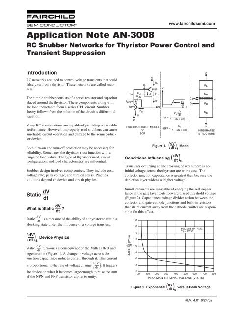
Static dV<br />
dt<br />
dV<br />
What is Static ?<br />
dt<br />
dV<br />
Static ------ is a measure of the ability of a thyristor to retain a<br />
dt<br />
blocking state under the influence of a voltage transient.<br />
dV<br />
( ) Device Physics<br />
dt s<br />
dV<br />
Static ------ turn-on is a consequence of the Miller effect <strong>and</strong><br />
dt<br />
regeneration (Figure 1). A change in voltage across the<br />
junction capacitance induces current through it. This current<br />
is proportional to the rate of voltage change ⎛dV<br />
------ ⎞<br />
⎝<br />
. It triggers<br />
dt ⎠<br />
the device on when it becomes large enough to raise the sum<br />
of the NPN <strong>and</strong> PNP transistor alphas to unity.<br />
I1<br />
ICN IJ<br />
NPN<br />
K<br />
CJP<br />
CJN<br />
IBN<br />
IK<br />
IBP<br />
IJ<br />
A<br />
IA<br />
PNP<br />
ICP<br />
I2<br />
TWO TR<strong>AN</strong>SISTOR MODEL<br />
OF<br />
SCR<br />
G<br />
V<br />
Figure 1.<br />
dV<br />
dt<br />
t<br />
dV<br />
CJ<br />
dt<br />
IA =<br />
1– (αN + αp)<br />
CJ<br />
CEFF =<br />
1– (αN + αp)<br />
dV<br />
(<br />
dt<br />
) s<br />
Model<br />
Small transients are incapable of charging the self-capacitance<br />
of the gate layer to its <strong>for</strong>ward biased threshold voltage<br />
(Figure 2). Capacitance voltage divider action between the<br />
collector <strong>and</strong> gate-cathode junctions <strong>and</strong> built-in resistors<br />
that shunt current away from the cathode emitter are responsible<br />
<strong>for</strong> this effect.<br />
CJ<br />
G<br />
A<br />
PE<br />
NB<br />
PB<br />
NE<br />
K<br />
C<br />
INTEGRATED<br />
STRUCTURE<br />
dV<br />
Conditions Influencing ( )<br />
dt s<br />
Transients occurring at line crossing or when there is no<br />
initial voltage across the thyristor are worst case. The<br />
collector junction capacitance is greatest then because the<br />
depletion layer widens at higher voltage.<br />
dV<br />
STATIC (V/µs)<br />
dt<br />
180<br />
160<br />
140<br />
120<br />
100<br />
80<br />
60<br />
40<br />
20<br />
20 100 200 300 400<br />
MAC 228-10 TRIAC<br />
TJ = 110°C<br />
500 600 700 800<br />
PEAK MAIN TERMINAL VOLTAGE (VOLTS)<br />
Figure 2. Exponential<br />
dV<br />
(<br />
dt<br />
) s<br />
versus Peak Voltage<br />
REV. 4.01 6/24/02
<strong>AN</strong>-<strong>3008</strong><br />
APPLICATION NOTE<br />
dV<br />
Static ------ does not depend strongly on voltage <strong>for</strong> operation<br />
dt<br />
below the maximum voltage <strong>and</strong> temperature rating.<br />
Avalanche multiplication will increase leakage current <strong>and</strong><br />
dV<br />
reduce ------ capability if a transient is within roughly 50 volts<br />
dt<br />
of the actual device breakover voltage.<br />
dV<br />
A higher rated voltage device guarantees increased ------ at<br />
dt<br />
lower voltage. This is a consequence of the exponential<br />
rating method where a 400 V device rated at 50 V/µs has a<br />
dV<br />
higher ------ to 200 V than a 200 V device with an identical<br />
dt<br />
rating. However, the same diffusion recipe usually applies<br />
<strong>for</strong> all voltages. So actual capabilities of the product are not<br />
much different.<br />
Heat increases current gain <strong>and</strong> leakage, lowering ⎛dV<br />
------ ⎞<br />
⎝<br />
,<br />
dt ⎠s<br />
the gate trigger voltage <strong>and</strong> noise immunity (Figure 3).<br />
dV<br />
STATIC (V/µs)<br />
dt<br />
180<br />
160<br />
140<br />
120<br />
100<br />
80<br />
60<br />
40<br />
Failure Mode<br />
MAC 228-10<br />
V PK = 800 V<br />
20<br />
20 100 200 300 400 500 600 700 800<br />
T J, JUNCTION TEMPERATURE (°C)<br />
dV<br />
Figure 3. Exponential (<br />
dt<br />
) versus Temperature<br />
s<br />
dV<br />
( )<br />
dt s<br />
dV<br />
Occasional unwanted turn-on by a transient may be acceptable<br />
in a heater circuit but isn’t in a fire prevention sprinkler<br />
system or <strong>for</strong> the control of a large motor. Turn-on is destructive<br />
when the follow-on current amplitude or rate is excessive.<br />
If the thyristor shorts the power line or charged<br />
capacitor, it will be damaged.<br />
Static ------ turn-on is non-destructive when series impedance<br />
dt<br />
limits the surge. The thyristor turns off after a half-cycle of<br />
dV<br />
conduction. High ------ aids current spreading in the thyristor,<br />
dt<br />
dI<br />
improving its ability to withst<strong>and</strong> ---- . Breakdown turn-on<br />
dt<br />
does not have this benefit <strong>and</strong> should be prevented.<br />
Improving<br />
dV<br />
( )<br />
dt s<br />
dV<br />
Static ------ can be improved by adding an external resistor<br />
dt<br />
from the gate to MT1 (Figure 4). The resistor provides a path<br />
dV<br />
<strong>for</strong> leakage <strong>and</strong> ------ induced currents that originate in the<br />
dt<br />
drive circuit or the thyristor itself.<br />
dV<br />
STATIC (V/µs)<br />
dt<br />
140<br />
120<br />
100<br />
80<br />
60<br />
40<br />
20<br />
MAC 228-10<br />
800V 110°C<br />
R INTERNAL = 600Ω<br />
0<br />
10 100 1000 10000<br />
GATE-MT 1, RESIST<strong>AN</strong>CE (OHMS)<br />
( ) s<br />
dV<br />
Figure 4. Exponential<br />
dt<br />
versus<br />
Gate to MT 1 Resistance<br />
Non-sensitive devices (Figure 5) have internal shorting<br />
resistors dispersed throughout the chip’s cathode area. This<br />
design feature improves noise immunity <strong>and</strong> high temperature<br />
blocking stability at the expense of increased trigger <strong>and</strong><br />
holding current. External resistors are optional <strong>for</strong> non-sensitive<br />
SCRs <strong>and</strong> TRIACs. They should be comparable in size<br />
to the internal shorting resistance of the device (20 to 100<br />
ohms) to provide maximum improvement. The internal resistance<br />
of the thyristor should be measured with an ohmmeter<br />
that does not <strong>for</strong>ward bias a diode junction.<br />
dV<br />
STATIC (V/µs)<br />
dt<br />
2200<br />
2000<br />
1800<br />
1600<br />
1400<br />
1200<br />
1000<br />
800<br />
600<br />
50 60 70 80 90 100 110 120 130<br />
T J, JUNCTION TEMPERATURE (°C)<br />
( ) s<br />
dV<br />
Figure 5. Exponential<br />
dt<br />
versus Junction Temperature<br />
MAC 16-8<br />
V PK = 600 V<br />
2 REV. 4.01 6/24/02
APPLICATION NOTE<br />
<strong>AN</strong>-<strong>3008</strong><br />
Sensitive gate TRIACS run 100 to 1000 ohms. With an gate drive circuit needs to be able to charge the capacitor<br />
dV<br />
without excessive delay, but it does not need to supply continuous<br />
current as it would <strong>for</strong> a resistor that increases ------<br />
external resistor, their ------ capability remains inferior to<br />
dt<br />
dV<br />
non-sensitive devices because lateral resistance within the<br />
dt<br />
dV<br />
dV<br />
Figure 7. Exponential ( versus<br />
Device Physics<br />
dt<br />
) s<br />
( )<br />
dt c<br />
gate layer reduces its benefit.<br />
the same amount. However, the capacitor does not enhance<br />
static thermal stability.<br />
Sensitive gate SCRs (I GT < 200 µA) have no built-in resistor.<br />
They should be used with an external resistor. The recommended<br />
value of the resistor is 1000 ohms. Higher values<br />
The maximum ⎛dV<br />
------ ⎞<br />
⎝<br />
improvement occurs with a short.<br />
dt ⎠s<br />
reduce maximum operating temperature ⎛dV<br />
Actual improvement stops be<strong>for</strong>e this because of spreading<br />
------ ⎞<br />
⎝<br />
(Figure 6).<br />
dt ⎠<br />
resistance in the thyristor. An external capacitor of about 0.1<br />
s<br />
The capability of these parts varies by more than 100 to 1 µF allows the maximum enhancement at a higher value of<br />
depending on gate-cathode termination.<br />
R GK .<br />
10 MEG<br />
MCR22-2<br />
One should keep the thyristor cool <strong>for</strong> the highest ⎛dV<br />
------ ⎞<br />
⎝<br />
.<br />
T A = 65°C<br />
dt ⎠s<br />
Also devices should be tested in the application circuit at the<br />
A<br />
10<br />
highest possible temperature using thyristors with the lowest<br />
1 MEG<br />
V G<br />
measured trigger current.<br />
K<br />
dV<br />
TRIAC Commutating<br />
dt<br />
100K<br />
dV<br />
What is Commutating ?<br />
dt<br />
dV<br />
The commutating ------ rating applies when a TRIAC has been<br />
dt<br />
conducting <strong>and</strong> attempts to turn-off with an inductive load.<br />
10K<br />
0.001 0.01 0.1 1 10 100 The current <strong>and</strong> voltage are out of phase (Figure 8). The<br />
dV<br />
TRIAC attempts to turn-off as the current drops below the<br />
STATIC (V/µs)<br />
dt<br />
holding value. Now the line voltage is high <strong>and</strong> in the opposite<br />
polarity to the direction of conduction. Successful turnoff<br />
requires the voltage across the TRIAC to rise to the<br />
dV<br />
Figure 6. Exponential ( versus<br />
dt<br />
) s<br />
Gate-Cathode Resistance<br />
instantaneous line voltage at a rate slow enough to prevent<br />
retriggering of the device.<br />
130<br />
R L<br />
120<br />
i 2<br />
V LINE<br />
MAC 228-10<br />
G<br />
V MT2-1<br />
110<br />
800V 110°C<br />
1<br />
dl<br />
100<br />
PHASE<br />
dt c<br />
90<br />
<strong>AN</strong>GLE<br />
φ<br />
80<br />
TIME<br />
TIME<br />
dV<br />
70<br />
i<br />
V LINE<br />
dt c<br />
60<br />
dV<br />
0.001 0.01<br />
0.1 1 Figure 8. TRIAC Inductive Load Turn-Off (<br />
dt<br />
)<br />
GATE TO MT 1, CAPACIT<strong>AN</strong>CE (µF)<br />
c<br />
Gate to MT 1 Capacitance<br />
A TRIAC functions like two SCRs connected in inverseparallel.<br />
So, a transient of either polarity turns it on.<br />
GATE-CATHODE RESIST<strong>AN</strong>CE (OHMS)<br />
dV<br />
STATIC (V/µs)<br />
dt<br />
A gate-cathode capacitor (Figure 7) provides a shunt path <strong>for</strong><br />
transient currents in the same manner as the resistor. It also<br />
filters noise currents from the drive circuit <strong>and</strong> enhances the<br />
built-in gate-cathode capacitance voltage divider effect. The<br />
VOLTAGE CURRENT<br />
There is charge within the crystal’s volume because of prior<br />
conduction (Figure 9). The charge at the boundaries of the<br />
VMT2-1<br />
REV. 4.01 6/24/02 3
<strong>AN</strong>-<strong>3008</strong><br />
APPLICATION NOTE<br />
collector junction depletion layer responsible <strong>for</strong> ⎛dV<br />
------ ⎞<br />
⎝<br />
is<br />
dt ⎠s<br />
also present. TRIACS have lower ⎛dV<br />
------ ⎞ than ⎛dV<br />
------ ⎞<br />
⎝<br />
because<br />
dt ⎠c<br />
⎝ dt ⎠s<br />
of this additional charge.<br />
P<br />
N<br />
N<br />
N N N<br />
REVERSE RECOVERY<br />
CURRENT PATH<br />
G<br />
MT 2<br />
+ –<br />
MT 1<br />
LATERAL VOLTAGE<br />
DROP<br />
Figure 9. TRIAC Structure <strong>and</strong><br />
Current Flow at Commutation<br />
TOP<br />
N N N<br />
Previously<br />
Conducting Side<br />
STORED CHARGE<br />
FROM POSITIVE<br />
CONDUCTION<br />
The volume charge storage within the TRIAC depends on<br />
the peak current be<strong>for</strong>e turn-off <strong>and</strong> its rate of zero crossing<br />
⎛dI<br />
----⎞<br />
⎝<br />
. In the classic circuit, the load impedance <strong>and</strong> line<br />
dt⎠c<br />
frequency determine ⎛dI<br />
----⎞<br />
⎝<br />
. The rate of crossing <strong>for</strong> sinusoidal<br />
currents is given by the slope of the secant line between<br />
dt⎠c<br />
the 50% <strong>and</strong> 0% levels as:<br />
⎛dI<br />
----⎞<br />
⎝dt⎠c<br />
6fI TM<br />
= --------------A/ms<br />
1000<br />
where f = line frequency <strong>and</strong> I TM = maximum on-state<br />
current in the TRIAC.<br />
Turn-off depends on both the Miller effect displacement<br />
dV<br />
current generated by ------ across the collector capacitance <strong>and</strong><br />
dt<br />
the currents resulting from internal charge storage within the<br />
volume of the device (Figure 10). If the reverse recovery<br />
current resulting from both these components is high, the<br />
lateral IR drop within the TRIAC base layer will <strong>for</strong>ward<br />
dV<br />
bias the emitter <strong>and</strong> turn the TRIAC on. Commutating ------<br />
dt<br />
capability is lower when turning off from the positive direction<br />
of current conduction because of device geometry. The<br />
gate is on the top of the die <strong>and</strong> obstructs current flow.<br />
Recombination takes place throughout the conduction period<br />
<strong>and</strong> along the back side of the current wave as it declines to zero.<br />
Turn-off capability depends on its shape. If the current amplitude<br />
is small <strong>and</strong> its zero crossing ⎛dI<br />
----⎞<br />
⎝<br />
is low, there is little<br />
dt⎠<br />
c<br />
volume charge storage <strong>and</strong> turn-off becomes limited by ⎛dV<br />
------ ⎞<br />
⎝<br />
.<br />
dt ⎠s<br />
At moderate current amplitudes, the volume charge begins<br />
to influence turn-off, requiring a larger snubber. When the<br />
current is large or has rapid zero crossing, ⎛dV<br />
------ ⎞<br />
⎝<br />
has little<br />
dt ⎠c<br />
dI<br />
influence. Commutating ---- <strong>and</strong> delay time to voltage<br />
dt<br />
reapplication determine whether turn-off will be successful<br />
or not. (Figures 11,12)<br />
VOLTAGE/CURRENT<br />
0<br />
Figure 10. TRIAC Current <strong>and</strong> Voltage at Commutation<br />
NORMALIZED DELAY TIME<br />
(td = W0 td)<br />
VMT2-1<br />
MAIN TERMINAL VOLTAGE (V)<br />
0.5<br />
0.2<br />
0.1<br />
0.05<br />
0.03<br />
0.02<br />
VOLUME<br />
STORAGE<br />
CHARGE<br />
V T<br />
E<br />
0<br />
dI<br />
dt<br />
c<br />
t d<br />
IRRM<br />
TIME<br />
dV<br />
dt<br />
Figure 11. <strong>Snubber</strong> Delay Time<br />
R L = 0<br />
M = 1<br />
I RRM = 0<br />
V<br />
DAMPING FACTOR<br />
0.2<br />
0.1<br />
c<br />
TIME<br />
CHARGE DUE<br />
TO dV/dt<br />
0.001 0.002 0.005 0.01 0.02 0.05 0.1 0.2 0.3 0.5 1<br />
V T<br />
E<br />
0.05<br />
0.02<br />
0.01<br />
0.005<br />
E<br />
Figure 12. Delay Time To Normalized Voltage<br />
4 REV. 4.01 6/24/02
APPLICATION NOTE<br />
<strong>AN</strong>-<strong>3008</strong><br />
Conditions Influencing<br />
dV<br />
Commutating ------ depends on charge storage <strong>and</strong> recovery<br />
dt<br />
dV<br />
dynamics in addition to the variables influencing static ------ .<br />
dt<br />
High temperatures increase minority carrier life-time <strong>and</strong> the<br />
size of recovery currents, making turn-off more difficult.<br />
Loads that slow the rate of current zero-crossing aid turn-off.<br />
Those with harmonic content hinder turn-off.<br />
Figure 13. Phase <strong>Control</strong>ling a Motor in a Bridge<br />
Circuit Examples<br />
Figure 13 shows a TRIAC controlling an inductive load in a<br />
bridge. The inductive load has a time constant longer than<br />
the line period. This causes the load current to remain constant<br />
<strong>and</strong> the TRIAC current to switch rapidly as the line<br />
voltage reverses. This application is notorious <strong>for</strong> causing<br />
TRIAC turn-off difficulty because of high ⎛dI<br />
----⎞<br />
⎝<br />
.<br />
dt⎠<br />
High currents lead to high junction temperatures <strong>and</strong> rates of<br />
current crossings. Motors can have 5 to 6 times the normal<br />
current amplitude at start-up. This increases both junction<br />
temperature <strong>and</strong> the rate of current crossing leading to turnoff<br />
problems.<br />
The line frequency causes high rates of current crossing in<br />
400 Hz applications. Resonant trans<strong>for</strong>mer circuits are doubly<br />
periodic <strong>and</strong> have current harmonics at both the primary<br />
<strong>and</strong> secondary resonance. Non-sinusoidal currents can lead<br />
to turn-off difficulty even if the current amplitude is low<br />
be<strong>for</strong>e zero-crossing.<br />
Failure Mode<br />
i<br />
C<br />
dV<br />
( )<br />
dt c<br />
R S<br />
L S<br />
dl<br />
dt<br />
i<br />
c DC MOTOR<br />
– +<br />
60 Hz R L<br />
t<br />
L<br />
> 8.3 µs<br />
R<br />
dV<br />
( )<br />
dt c<br />
⎛dV<br />
------ ⎞<br />
⎝<br />
failure causes a loss of phase control. Temporary turnon<br />
or total turn-off failure is possible. This can be destructive<br />
dt ⎠c<br />
if the TRIAC conducts asymmetrically causing a dc current<br />
component <strong>and</strong> magnetic saturation. The winding resistance<br />
limits the current. Failure results because of excessive surge<br />
current <strong>and</strong> junction temperature.<br />
c<br />
dV<br />
Improving ( )<br />
dt c<br />
The same steps that improve ⎛dV<br />
------ ⎞ aid ⎛dV<br />
------ ⎞<br />
⎝<br />
except when<br />
dt ⎠s<br />
⎝ dt ⎠c<br />
stored charge dominates turn-off. Steps that reduce the<br />
stored charge or soften the commutation are necessary then.<br />
Larger TRIACS have better turn-off capability than smaller<br />
ones with a given load. The current density is lower in the<br />
larger device allowing recombination to claim a greater proportion<br />
of the internal charge. Also junction temperatures are<br />
lower.<br />
TRIACS with high gate trigger current have greater turn-off<br />
ability because of lower spreading resistance in the gate<br />
layer, reduced Miller effect, or shorter lifetime.<br />
The rate of current crossing can be adjusted by adding a<br />
commutation softening inductor in series with the load.<br />
Small high permeability “square loop” inductors saturate<br />
causing no significant disturbance to the load current. The<br />
inductor resets as the current crosses zero introducing a large<br />
inductor into the snubber circuit at that time. This slows the<br />
current crossing <strong>and</strong> delays the reapplication of blocking<br />
voltage aiding turn-off.<br />
The commutation inductor is a circuit element that introduces<br />
time delay, as opposed to inductance, into the circuit.<br />
dV<br />
It will have little influence on observed ------ at the device.<br />
dt<br />
The following example illustrates the improvement resulting<br />
from the addition of an inductor constructed by winding 33<br />
turns of number 18 wire on a tape wound core (52000 -1A).<br />
This core is very small having an outside diameter of 3/4<br />
inch <strong>and</strong> a thickness of 1/8 inch. The delay time can be calculated<br />
from:<br />
( N A B 10 – 8 )<br />
t s = -------------------------------- where:<br />
E<br />
t s = time delay to saturation in seconds.<br />
B = saturating flux density in Gauss<br />
A = effective core cross sectional area in cm 2<br />
N = number of turns.<br />
For the described inductor:<br />
t s = (33 turns)(0.076 cm 2 )(28000 Gauss)(1 x 10 -8 )/(175 v) = 4.0 µs.<br />
The saturation current of the inductor does not need to be<br />
much larger than the TRIAC trigger current. Turn-off failure<br />
will result be<strong>for</strong>e recovery currents become greater than this<br />
value. This criterion allows sizing the inductor with the<br />
following equation:<br />
REV. 4.01 6/24/02 5
<strong>AN</strong>-<strong>3008</strong><br />
APPLICATION NOTE<br />
I S<br />
H S M L<br />
= ------------------ where:<br />
0.4 π N<br />
H S = MMF to saturate = 0.5 Oersted<br />
ML = mean magnetic path length = 4.99 cm.<br />
(.5) (4.99)<br />
I S = ----------------------- = 60 mA.<br />
0.4 π 33<br />
<strong>Snubber</strong> Physics<br />
Undamped Natural Resonance<br />
I<br />
ω 0 = -----------Radians/second<br />
LC<br />
dV<br />
Resonance determines ------ <strong>and</strong> boosts the peak capacitor<br />
dt<br />
voltage when the snubber resistor is small. C <strong>and</strong> L are<br />
related to one another by ω 2 dV<br />
0 . ------ scales linearly with ω<br />
dt<br />
0<br />
when the damping factor is held constant. A ten to one<br />
dV<br />
reduction in ------ requires a 100 to 1 increase in either<br />
dt<br />
component.<br />
Damping Factor<br />
ρ =<br />
The damping factor is proportional to the ratio of the circuit<br />
loss <strong>and</strong> its surge impedance. It determines the trade off<br />
dV<br />
between ------ <strong>and</strong> peak voltage. Damping factors between<br />
dt<br />
0.01 <strong>and</strong> 1.0 are recommended.<br />
The <strong>Snubber</strong> Resistor<br />
dV<br />
Damping <strong>and</strong><br />
dt<br />
dV<br />
When ρ < 0.5, the snubber resistor is small, <strong>and</strong> ------ depends<br />
dt<br />
dV<br />
mostly on resonance. There is little improvement in ------ <strong>for</strong><br />
dt<br />
damping factors less than 0.3, but peak voltage <strong>and</strong> snubber<br />
discharge current increase. The voltage wave has a 1-COS(θ)<br />
dV<br />
shape with overshoot <strong>and</strong> ringing. Maximum ------ occurs at a<br />
dt<br />
time later than t = 0. There is a time delay be<strong>for</strong>e the<br />
voltage rise, <strong>and</strong> the peak voltage almost doubles.<br />
When ρ > 0.5, the voltage wave is nearly exponential in<br />
dV<br />
shape. The maximum instantaneous ------ occurs at t = 0.<br />
dt<br />
There is little time delay <strong>and</strong> moderate voltage overshoot.<br />
R<br />
---<br />
2<br />
dV<br />
When ρ > 1.0, the snubber resistor is large <strong>and</strong> ------ depends<br />
dt<br />
mostly on its value. There is some overshoot even though the<br />
circuit is overdamped.<br />
C<br />
---<br />
L<br />
High load inductance requires large snubber resistors <strong>and</strong><br />
small snubber capacitors. Low inductances imply small<br />
resistors <strong>and</strong> large capacitors.<br />
Damping <strong>and</strong> Transient Voltages<br />
Figure 14 shows a series inductor <strong>and</strong> filter capacitor<br />
connected across the ac main line. The peak to peak voltage<br />
of a transient disturbance increases by nearly four times.<br />
Also the duration of the disturbance spreads because of<br />
ringing, increasing the chance of malfunction or damage to<br />
the voltage sensitive circuit. Closing a switch causes this<br />
behavior. The problem can be reduced by adding a damping<br />
resistor in series with the capacitor.<br />
+700<br />
V (VOLTS)<br />
0<br />
-700<br />
0<br />
10µs<br />
340 V<br />
100µH 0.05<br />
0.1<br />
µF<br />
0 10 20<br />
TIME (µs)<br />
Figure 14. Undamped LC Filter<br />
Magnifies <strong>and</strong> Lengthens a Transient<br />
dl<br />
dt<br />
Non-Inductive Resistor<br />
The snubber resistor limits the capacitor discharge current<br />
dI<br />
dI<br />
<strong>and</strong> reduces ---- stress. High ---- destroys the thyristor even<br />
dt<br />
dt<br />
though the pulse duration is very short. The rate of current<br />
rise is directly proportional to circuit voltage <strong>and</strong> inversely<br />
proportional to series inductance. The snubber is often the<br />
major offender because of its low inductance <strong>and</strong> close<br />
proximity to the thyristor.<br />
With no transient suppressor, breakdown of the thyristor sets<br />
the maximum voltage on the capacitor. It is possible to<br />
exceed the highest rated voltage in the device series because<br />
high voltage devices are often used to supply low voltage<br />
specifications.<br />
The minimum value of the snubber resistor depends on the<br />
type of thyristor, triggering quadrants, gate current amplitude,<br />
voltage, repetitive or non-repetitive operation <strong>and</strong><br />
required life expectancy. There is no simple way to predict<br />
the rate of current rise because it depends on turn-on speed<br />
of the thyristor, circuit layout, type <strong>and</strong> size of snubber<br />
capacitor, <strong>and</strong> inductance in the snubber resistor. The<br />
equations in Appendix D describes the circuit. However,<br />
V<br />
VOLTAGE<br />
SENSITIVE<br />
CI<strong>RC</strong>UIT<br />
6 REV. 4.01 6/24/02
APPLICATION NOTE<br />
<strong>AN</strong>-<strong>3008</strong><br />
the values required <strong>for</strong> the model are not easily obtained<br />
except by testing. There<strong>for</strong>e, reliability should be verified in<br />
the actual application circuit.<br />
Table 1 shows suggested minimum resistor values estimated<br />
(Appendix A) by testing a 20 piece sample from the four<br />
different TRIAC die sizes.<br />
Table 1. Minimum Non-inductive <strong>Snubber</strong> Resistor <strong>for</strong><br />
Four Quadrant Triggering.<br />
Peak V C<br />
TRIAC Type Volts<br />
Non-Sensitive 200<br />
Gate<br />
300<br />
(I GT > 10mA) 400<br />
8 to 40 A (RMS) 600<br />
800<br />
R S Ohms<br />
3.3<br />
6.8<br />
11<br />
39<br />
51<br />
dl<br />
dt<br />
A/µS<br />
170<br />
250<br />
308<br />
400<br />
400<br />
dl<br />
Reducing<br />
dt<br />
dI<br />
TRIAC ---- can be improved by avoiding quadrant 4<br />
dt<br />
triggering. Most optocoupler circuits operate the TRIAC in<br />
quadrants 1 <strong>and</strong> 3. Integrated circuit drivers use quadrants 2<br />
<strong>and</strong> 3. Zero crossing trigger devices are helpful because they<br />
prohibit triggering when the voltage is high.<br />
Driving the gate with a high amplitude fast rise pulse<br />
dI<br />
increases ---- capability. The gate ratings section defines the<br />
dt<br />
maximum allowed current.<br />
dI<br />
Inductance in series with the snubber capacitor reduces ---- .<br />
dt<br />
It should not be more than five percent of the load inductance<br />
dV<br />
to prevent degradation of the snubber’s ------ suppression<br />
dt<br />
capability. Wirewound snubber resistors sometimes serve<br />
this purpose. Alternatively, a separate inductor can be added<br />
in series with the snubber capacitor. It can be small because<br />
it does not need to carry the load current. For example, 18<br />
turns of AWG No. 20 wire on a T50-3 (1/2 inch) powdered<br />
iron core creates a non-saturating 6.0 µH inductor.<br />
A 10 ohm, 0.33 µF snubber charged to 650 volts resulted in a<br />
dI<br />
1000 A/µs ---- . Replacement of the non-inductive snubber<br />
dt<br />
resistor with a 20 watt wirewound unit lowered the rate of<br />
rise to a non-destructive 170 A/µs at 800 V. The inductor<br />
gave an 80 A/µs rise at 800 V with the non-inductive resistor.<br />
The <strong>Snubber</strong> Capacitor<br />
A damping factor of 0.3 minimizes the size of the snubber<br />
dV<br />
capacitor <strong>for</strong> a given value of ------ . This reduces the cost <strong>and</strong><br />
dt<br />
physical dimensions of the capacitor. However, it raises<br />
voltage causing a counter balancing cost increase.<br />
<strong>Snubber</strong> operation relies on the charging of the snubber<br />
capacitor. Turn-off snubbers need a minimum conduction<br />
angle long enough to discharge the capacitor. It should be at<br />
least several time constants (R S C S ).<br />
Stored Energy<br />
Inductive Switching Transients<br />
1 2<br />
E -- L I<br />
2 O Watt-seconds or Joules<br />
I O = current in Amperes flowing in the inductor at t = 0.<br />
=<br />
R<br />
V PK<br />
C<br />
Resonant charging cannot boost the supply voltage at turnoff<br />
by more than 2. If there is an initial current flowing in the<br />
load inductance at turn-off, much higher voltages are possible.<br />
Energy storage is negligible when a TRIAC turns off<br />
because of its low holding or recovery current.<br />
The presence of an additional switch such as a relay, thermostat<br />
or breaker allows the interruption of load current <strong>and</strong> the<br />
generation of high spike voltages at switch opening. The<br />
energy in the inductance transfers into the circuit capacitance<br />
<strong>and</strong> determines the peak voltage (Figure 15).<br />
dV<br />
dt<br />
L<br />
I<br />
= V PK = I<br />
C<br />
L<br />
C<br />
(a.) Protected Circuit<br />
I<br />
OPTIONAL<br />
FAST<br />
SLOW<br />
(b.) Unprotected Circuit<br />
Figure 15. Interrupting Inductive Load Current<br />
Capacitor Discharge<br />
⎛ 1<br />
The energy stored in the snubber capacitor E C = --CV 2 ⎞<br />
⎝ 2 ⎠<br />
transfers to the snubber resistor <strong>and</strong> thyristor every time it<br />
turns on. The power loss is proportional to frequency<br />
(P AV = 120 E C @ 60 H Z ).<br />
Current Diversion<br />
The current flowing in the load inductor cannot change<br />
instantly. This current diverts through the snubber resistor<br />
dV<br />
causing a spike of theoretically infinite ------ with magnitude<br />
dt<br />
equal to (I RRM R) or (I H R).<br />
Load Phase Angle<br />
Highly inductive loads cause increased voltage <strong>and</strong> ⎛dV<br />
------ ⎞<br />
⎝<br />
at<br />
dt ⎠c<br />
turn-off. However, they help to protect the thyristor from<br />
transients <strong>and</strong> ⎛dV<br />
------ ⎞<br />
⎝<br />
. The load serves as the snubber<br />
dt ⎠<br />
s<br />
REV. 4.01 6/24/02 7
<strong>AN</strong>-<strong>3008</strong><br />
APPLICATION NOTE<br />
inductor <strong>and</strong> limits the rate of inrush current if the device<br />
dV<br />
does turn on. Resistance in the load lowers ------ <strong>and</strong> V<br />
dt PK<br />
(Figure 16).<br />
/ (E W0)<br />
dV<br />
dt<br />
dV<br />
dt<br />
NORMALIZED<br />
1.4 2.2<br />
E<br />
dV 2.1<br />
dt<br />
1.2<br />
2<br />
1.9<br />
1<br />
1.8<br />
M = 1<br />
M = 0.75<br />
1.7<br />
V PK<br />
0.8<br />
0.6<br />
0.4<br />
0.2<br />
M = R S / (R L + R S)<br />
0<br />
0 0.2 0.4 0.6 0.8 1<br />
DAMPING FACTOR<br />
R<br />
M = RESISTIVE DIVISION RATIO = S<br />
R L + R S<br />
I RRM = 0<br />
Figure 16. 0 to 63%<br />
M = 0.5<br />
M = 0.25<br />
M = 0<br />
dV<br />
dt<br />
Characteristics Voltage Waves<br />
NORMALIZED PEAK VOLTAGE<br />
VPK/E<br />
Damping factor <strong>and</strong> reverse recovery current determine the<br />
shape of the voltage wave. It is not exponential when the<br />
snubber damping factor is less than 0.5 (Figure 17) or when<br />
significant recovery currents are present.<br />
VMT2-1 (VOLTS)<br />
500<br />
400<br />
ρ = 0 ρ = 0.1<br />
300<br />
0.1<br />
200 0.3<br />
1<br />
ρ = 0.3 ρ = 1<br />
100<br />
0<br />
0<br />
0<br />
0.7 1.4 2.1 2.8 3.5 4.2 4.9 5.6 6.3 7<br />
TIME (µs)<br />
dV<br />
0-63% = 100 V/µs, E = 250 V,<br />
dt s<br />
R L = 0, I RRM = 0<br />
1.6<br />
1.5<br />
1.4<br />
1.3<br />
1.2<br />
1.1<br />
1<br />
0.9<br />
NORMALIZED PEAK VOLTAGE <strong>AN</strong>D dV<br />
dt<br />
2.8<br />
2.6<br />
2.4<br />
2.2<br />
2.0<br />
1.8<br />
1.6<br />
1.4<br />
1.2<br />
1.0<br />
0.8<br />
0.6<br />
0.4<br />
0.2<br />
Figure 18. Trade-Off Between V PK <strong>and</strong><br />
dV<br />
A variety of wave parameters (Figure 18) describe ------ .<br />
dt<br />
Some are easy to solve <strong>for</strong> <strong>and</strong> assist underst<strong>and</strong>ing. These<br />
dV<br />
dV<br />
include the initial ------ , the maximum instantaneous ------ , <strong>and</strong><br />
dt<br />
dt<br />
dV<br />
the average ------ to the peak reapplied voltage. The 0 to 63%<br />
dt<br />
⎛dV<br />
------ ⎞ <strong>and</strong> 10 to 63% ⎛dV<br />
------ ⎞<br />
⎝<br />
definitions on device data sheets<br />
dt ⎠s<br />
⎝ dt ⎠c<br />
are easy to measure but difficult to compute.<br />
Non-Ideal Behaviors<br />
Core Losses<br />
10-63%<br />
dV<br />
dt<br />
0<br />
0 0.2 0.4 0.6 0.8 1.0 2.2 1.4 1.6 1.8 2.0<br />
DAMPING FACTOR ( ρ )<br />
(R L = 0, M = 1, I RRM = 0)<br />
NORMALIZED<br />
dV<br />
=<br />
dt<br />
dV<br />
dt<br />
dV<br />
dt<br />
E<br />
dV/dt<br />
E ω 0<br />
MAX<br />
o<br />
0-63%<br />
dV<br />
dt<br />
V PK<br />
10-63%<br />
NORMALIZED V PK<br />
= VPK<br />
E<br />
dV<br />
dt<br />
The magnetic core materials in typical 60 Hz loads introduce<br />
losses at the snubber natural frequency. They appear as a<br />
resistance in series with the load inductance <strong>and</strong> winding dc<br />
dV<br />
resistance (Figure 19). This causes actual ------ to be less than<br />
dt<br />
the theoretical value.<br />
Figure 17. Voltage Waves <strong>for</strong> Different Damping Factors<br />
8 REV. 4.01 6/24/02
APPLICATION NOTE<br />
<strong>AN</strong>-<strong>3008</strong><br />
L<br />
C<br />
R<br />
Core remanence <strong>and</strong> saturation cause surge currents. They<br />
depend on trigger angle, line impedance, core characteristics,<br />
<strong>and</strong> direction of the residual magnetization. For example,<br />
a 2.8 kVA 120 V 1:1 trans<strong>for</strong>mer with a 1.0 ampere load<br />
produced 160 ampere currents at start-up. Soft starting the<br />
circuit at a small conduction angle reduces this current.<br />
L DEPENDS ON CURRENT AMPLITUDE, CORE<br />
SATURATION<br />
R INCLUDES CORE LOSS, WINDING R. INCREASES<br />
WITH FREQUENCY<br />
C WINDING CAPACIT<strong>AN</strong>CE. DEPENDS ON<br />
INSULATION, WIRE SIZE, GEOMETRY<br />
Complex Loads<br />
Figure 19. Inductor Model<br />
Many real-world inductances are non-linear. Their core<br />
materials are not gapped causing inductance to vary with<br />
current amplitude. Small signal measurements poorly<br />
characterize them. For modeling purposes, it is best to<br />
measure them in the actual application.<br />
Complex load circuits should be checked <strong>for</strong> transient voltages<br />
<strong>and</strong> currents at turn-on <strong>and</strong> turn-off. With a capacitive<br />
load, turn-on at peak input voltage causes the maximum<br />
surge current. Motor starting current runs 4 to 6 times the<br />
steady state value. Generator action can boost voltages above<br />
the line value. Inc<strong>and</strong>escent lamps have cold start currents 10<br />
to 20 times the steady state value. Trans<strong>for</strong>mers generate<br />
voltage spikes when they are energized. <strong>Power</strong> factor correction<br />
circuits <strong>and</strong> switching devices create complex loads. In most<br />
cases, the simple CRL model allows an approximate snubber<br />
design. However, there is no substitute <strong>for</strong> testing <strong>and</strong> measuring<br />
the worst case load conditions.<br />
Surge Currents in Inductive Circuits<br />
Inductive loads with long L/R time constants cause asymmetric<br />
multi-cycle surges at start up (Figure 20). Triggering<br />
at zero voltage crossing is the worst case condition. The<br />
surge can be eliminated by triggering at the zero current<br />
crossing angle.<br />
i (AMPERES)<br />
90<br />
0<br />
240<br />
VAC<br />
40<br />
20 MHY<br />
i<br />
0.1<br />
Ω<br />
ZERO VOLTAGE TRIGGERING, I RMS = 30 A<br />
80 120 160 200<br />
TIME (MILLISECONDS)<br />
Figure 20. Start-Up Surge For Inductive Circuit<br />
Trans<strong>for</strong>mer cores are usually not gapped <strong>and</strong> saturate<br />
easily. A small asymmetry in the conduction angle causes<br />
magnetic saturation <strong>and</strong> multi-cycle current surges.<br />
Steps to achieve reliable operation include:<br />
1. Supply sufficient trigger current amplitude. TRIACS<br />
have different trigger currents depending on their quadrant<br />
of operation. Marginal gate current or optocoupler<br />
LED current causes halfwave operation.<br />
2. Supply sufficient gate current duration to achieve<br />
latching. Inductive loads slow down the main terminal<br />
current rise. The gate current must remain above the<br />
specified I GT until the main terminal current exceeds the<br />
latching value. Both a resistive bleeder around the load<br />
<strong>and</strong> the snubber discharge current help latching.<br />
3. Use a snubber to prevent TRIAC ⎛dV<br />
------ ⎞<br />
⎝<br />
failure.<br />
dt ⎠c<br />
4. Minimize designed-in trigger asymmetry. Triggering<br />
must be correct every half-cycle including the first.<br />
Use a storage scope to investigate circuit behavior<br />
during the first few cycles of turn-on. Alternatively,<br />
get the gate circuit up <strong>and</strong> running be<strong>for</strong>e energizing<br />
the load.<br />
5. Derive the trigger synchronization from the line instead<br />
of the TRIAC main terminal voltage. This avoids regenerative<br />
interaction between the core hysteresis <strong>and</strong> the<br />
triggering angle preventing trigger runaway, halfwave<br />
operation, <strong>and</strong> core saturation.<br />
6. Avoid high surge currents at start-up. Use a current<br />
probe to determine surge amplitude. Use a soft start<br />
circuit to reduce inrush current.<br />
Distributed Winding Capacitance<br />
There are small capacitances between the turns <strong>and</strong> layers of<br />
a coil. Lumped together, they model as a single shunt capacitance.<br />
The load inductor behaves like a capacitor at frequencies<br />
above its self-resonance. It becomes ineffective in<br />
dV<br />
controlling ------ <strong>and</strong> V PK when a fast transient such as that<br />
dt<br />
resulting from the closing of a switch occurs. This problem<br />
can be solved by adding a small snubber across the line.<br />
Self-Capacitance<br />
dV<br />
A thyristor has self-capacitance which limits ------ when the<br />
dt<br />
load inductance is large. Large load inductances, high power<br />
factors, <strong>and</strong> low voltages may allow snubberless<br />
operation.<br />
REV. 4.01 6/24/02 9
<strong>AN</strong>-<strong>3008</strong><br />
<strong>Snubber</strong> Examples<br />
Without Inductance<br />
<strong>Power</strong> TRIAC Example<br />
Figure 2l shows a transient voltage applied to a TRIAC<br />
controlling a resistive load. Theoretically there will be an<br />
instantaneous step of voltage across the TRIAC. The only<br />
elements slowing this rate are the inductance of the wiring<br />
<strong>and</strong> the self-capacitance of the thyristor. There is an exponential<br />
capacitor charging component added along with a<br />
decaying component because of the IR drop in the snubber<br />
resistor. The non-inductive snubber circuit is useful when the<br />
load resistance is much larger than the snubber resistor.<br />
R L<br />
10V/µs<br />
R in 1<br />
6 180 2.4k<br />
V CC<br />
2 MOC R 1 R 2<br />
3020 0.1µF C1<br />
3021 4<br />
0.63 (170)<br />
φ CNTL<br />
DESIGN<br />
dV<br />
dt<br />
APPLICATION NOTE<br />
T2322D<br />
1V/µs<br />
(0.63) (170)<br />
= = 0.45V/µs<br />
(2400) (0.1µF)<br />
TIME<br />
240µs<br />
dV<br />
dt (V/µs)<br />
<strong>Power</strong> TRIAC<br />
Optocoupler<br />
0.99 0.35<br />
1A, 60Hz<br />
L = 318 MHY<br />
170V<br />
E<br />
e<br />
R S<br />
C S<br />
Figure 22. Single <strong>Snubber</strong> For Sensitive Gate TRIAC <strong>and</strong><br />
Phase <strong>Control</strong>lable Optocoupler (ρ = 0.67)<br />
e<br />
E<br />
t = 0<br />
V step = E<br />
R S<br />
R S + R L<br />
TIME<br />
τ = (R L + R S) C S<br />
e(t = o+) = E<br />
R S<br />
R S + R L<br />
e – t/τ + (1 – e – t/τ )<br />
RESISTOR CAPACITOR<br />
COMPONENT COMPONENT<br />
The optocoupler conducts current only long enough to trigger<br />
the power device. When it turns on, the voltage between<br />
MT2 <strong>and</strong> the gate drops below the <strong>for</strong>ward threshold voltage<br />
of the opto-TRIAC causing turn-off. The optocoupler sees<br />
⎛dV<br />
------ ⎞<br />
⎝<br />
when the power TRIAC turns off later in the conduction<br />
cycle at zero current crossing. There<strong>for</strong>e, it is not neces-<br />
dt ⎠s<br />
sary to design <strong>for</strong> the lower optocoupler ⎛dV<br />
------ ⎞<br />
⎝<br />
rating. In this<br />
dt ⎠c<br />
example, a single snubber designed <strong>for</strong> the optocoupler<br />
protects both devices.<br />
Figure 21. Non-inductive <strong>Snubber</strong> Circuit<br />
Opto-TRIAC Examples<br />
Single <strong>Snubber</strong>, Time Constant Design<br />
Figure 22 illustrates the use of the <strong>RC</strong> time constant design<br />
method. The optocoupler sees only the voltage across the<br />
snubber capacitor. The resistor R 1 supplies the trigger<br />
current of the power TRIAC. A worst case design procedure<br />
assumes that the voltage across the power TRIAC changes<br />
instantly. The capacitor voltage rises to 63% of the maximum<br />
in one time constant. Then:<br />
0.63 E dV<br />
R 1 C S = τ = --------------- where ⎛------<br />
⎞ is the rated static dV ------<br />
⎛dV<br />
⎝<br />
------ ⎞ dt ⎠s<br />
dt<br />
⎝ dt ⎠s<br />
<strong>for</strong> the optocoupler.<br />
V CC<br />
1<br />
2<br />
3<br />
MOC3031<br />
4<br />
5<br />
6<br />
100<br />
1N4001<br />
51<br />
MCR265-4<br />
MCR265-4<br />
100<br />
1N4001<br />
(50 V/µs SNUBBER, ρ = 1.0)<br />
0.022<br />
µF<br />
Figure 23. Anti-Parallel SCR Driver<br />
1MHY<br />
430<br />
120V<br />
400 Hz<br />
Octocouplers with SCRs<br />
dV<br />
Anti-parallel SCR circuits result in the same ------ across the<br />
dt<br />
optocoupler <strong>and</strong> SCR (Figure 23). Phase controllable optocouplers<br />
require the SCRs to be snubbed to their lower ------<br />
dV<br />
dt<br />
rating. Anti-parallel SCR circuits are free from the charge<br />
storage behaviors that reduce the turn-off capability of<br />
TRIACs. Each SCR conducts <strong>for</strong> a half-cycle <strong>and</strong> has the<br />
next half cycle of the ac line in which to recover. The turn-off<br />
dV<br />
------ of the conducting SCR becomes a static <strong>for</strong>ward blocking<br />
------ <strong>for</strong> the other device. Use the SCR data sheet ⎛dV<br />
------ ⎞<br />
dt<br />
dV<br />
dt<br />
⎝ dt ⎠s<br />
rating in the snubber design.<br />
10 REV. 4.01 6/24/02
APPLICATION NOTE<br />
<strong>AN</strong>-<strong>3008</strong><br />
A SCR used inside a rectifier bridge to control an ac load<br />
will not have a half cycle in which to recover. The available<br />
time decreases with increasing line voltage. This makes the<br />
circuit less attractive. Inductive transients can be suppressed<br />
by a snubber at the input to the bridge or across the SCR.<br />
However, the time limitation still applies.<br />
The current through the snubber resistor is:<br />
t<br />
V ⎛ – -<br />
τ⎞ i ----- ⎜1–<br />
e ⎟ ,<br />
R τ ⎝ ⎠<br />
<strong>and</strong> the voltage across the TRAIC is:<br />
=<br />
dV<br />
( ) c<br />
dV<br />
Opto<br />
dt<br />
Zero-crossing optocouplers can be used to switch inductive<br />
loads at currents less than 100 mA (Figure 24). However a<br />
power TRIAC along with the optocoupler should be used <strong>for</strong><br />
higher load currents.<br />
LOAD CURRENT (mA RMS)<br />
80<br />
70<br />
60<br />
50<br />
40<br />
30<br />
20<br />
10<br />
C S = 0.01<br />
C S = 0.001<br />
NO SNUBBER<br />
0<br />
20 30 40 50 60 70 80 90 100<br />
T A, AMBIENT TEMPERATURE (°C)<br />
(R S = 100Ω, V RMS = 220V, POWER FACTOR = 0.5)<br />
Figure 24. MOC3062 Inductive Load Current versus T A<br />
A phase controllable optocoupler is recommended with a<br />
power device. When the load current is small, a MAC97<br />
TRIAC is suitable.<br />
Unusual circuit conditions sometimes lead to unwanted<br />
operation of an optocoupler in ⎛dV<br />
------ ⎞<br />
⎝<br />
mode. Very large<br />
dt ⎠c<br />
currents in the power device cause increased voltages<br />
between MT2 <strong>and</strong> the gate that hold the optocoupler on.<br />
Use of a larger TRIAC or other measures that limit inrush<br />
current solve this problem.<br />
Very short conduction times leave residual charge in the<br />
optocoupler. A minimum conduction angle allows recovery<br />
be<strong>for</strong>e voltage reapplication.<br />
The <strong>Snubber</strong> with Inductance<br />
Consider an overdamped snubber using a large capacitor<br />
whose voltage changes insignificantly during the time under<br />
consideration. The circuit reduces to an equivalent L/R series<br />
charging circuit.<br />
e = i R S<br />
The voltage wave across the TRIAC has an exponential rise<br />
with maximum rate at t = 0. Taking its derivative gives its<br />
value as:<br />
⎛------<br />
⎞<br />
⎝ dt ⎠0<br />
VR<br />
= ---------- S<br />
L<br />
Highly overdamped snubber circuits are not practical<br />
designs. The example illustrates several properties:<br />
1. The initial voltage appears completely across the circuit<br />
inductance. Thus, it determines the rate of change of<br />
dV<br />
current through the snubber resistor <strong>and</strong> the initial ------ .<br />
dt<br />
This result does not change when there is resistance in<br />
the load <strong>and</strong> holds true <strong>for</strong> all damping factors.<br />
2. The snubber works because the inductor controls the<br />
rate of current change through the resistor <strong>and</strong> the rate<br />
of capacitor charging. <strong>Snubber</strong> design cannot ignore the<br />
inductance. This approach suggests that the snubber<br />
capacitance is not important but that is only true <strong>for</strong><br />
this hypothetical condition. The snubber resistor shunts<br />
the thyristor causing unacceptable leakage when the<br />
capacitor is not present. If the power loss is tolerable,<br />
dV<br />
------ can be controlled without the capacitor. An example<br />
dt<br />
is the soft-start circuit used to limit inrush current in<br />
switching power supplies (Figure 25).<br />
E<br />
E<br />
AC LINE SNUBBER<br />
L<br />
AC LINE SNUBBER<br />
L<br />
<strong>Snubber</strong> with no C<br />
RECTIFIER<br />
BRIDGE<br />
dV<br />
dt<br />
R S<br />
= ERS<br />
φ L<br />
R S<br />
Figure 25. Surge Current Limiting<br />
For a Switching <strong>Power</strong> Supply<br />
G<br />
G<br />
RECTIFIER<br />
BRIDGE<br />
C1<br />
C1<br />
REV. 4.01 6/24/02 11
<strong>AN</strong>-<strong>3008</strong><br />
APPLICATION NOTE<br />
TRIAC Design Procedure<br />
dV<br />
(<br />
dt<br />
) c<br />
dV<br />
1. Refer to Figure 18 <strong>and</strong> select a particular damping factor<br />
(ρ)giving a suitable trade-off between V PK <strong>and</strong> ------ .<br />
dt<br />
dV<br />
Determine the normalized ------ corresponding to the<br />
dt<br />
chosen damping factor.<br />
The volage E depends on the load phase angle:<br />
E 2 V RMS Sin (φ) where φ = tan – 1 X =<br />
⎛------<br />
L ⎞ where<br />
⎝R L<br />
⎠<br />
φ = measured phase angle between line V <strong>and</strong> load I<br />
R L = measured dc resistance of the load.<br />
dV<br />
( Safe Area Curve<br />
dt<br />
) c<br />
dV<br />
Figure 26 shows a MAC16 TRIAC turn-off safe operating<br />
area curve. Turn-off occurs without problem under the curve.<br />
The region is bounded by static ------ at low values of ⎛dI<br />
----⎞<br />
dt<br />
⎝dt⎠c<br />
<strong>and</strong> delay time at high currents. Reduction of the peak current<br />
permits operation at higher line frequency. This TRIAC<br />
operated at f = 400 Hz, T J = 125 °C, <strong>and</strong> I TM = 6.0 amperes<br />
using a 30 ohm <strong>and</strong> 0.068 µF snubber. Low damping factors<br />
extend operation to higher ⎛dI<br />
----⎞<br />
⎝<br />
, but capacitor sizes<br />
dt⎠c<br />
increase. The addition of a small, saturable commutation<br />
inductor extends the allowed current rate by introducing<br />
recovery delay time.<br />
Then<br />
V RMS 2 2<br />
Z -------------- R<br />
I L + X L X L Z 2 2<br />
= = – R L <strong>and</strong><br />
RMS<br />
X<br />
L = --------------------- L<br />
2 π f Line<br />
If only the load current is known, assume a pure<br />
inductance. This gives a conservative design. Then:<br />
V RMS<br />
L = --------------------------------------- where E = 2 V<br />
2 π f LINE I RMS<br />
RMS<br />
For Example:<br />
120<br />
E = 2 120 = 170 V; L = ----------------------------------- = 39.8 mH<br />
( 8 A) ( 377 rps)<br />
(V/µs)<br />
100<br />
10<br />
c<br />
dV<br />
dt<br />
1<br />
0.1<br />
10<br />
dl<br />
dt<br />
-ITM = 15A<br />
c = 6 f ITM x 10-3 A/ms<br />
WITH COMMUTATION L<br />
14 18 22 26 30 34 38 42 46 50<br />
dV<br />
AMPERES/MILLISECOND<br />
dt c<br />
MAC 16-8, COMMUTATIONAL L = 33 TURNS #18,<br />
52000-1A TAPE WOUND CORE 3/4 INCH OD<br />
Read from the graph at ρ = 0.6, V PK = (1.25) 170 = 213V.<br />
dV<br />
Use 400V TRIAC. Read ------ = 1.0<br />
dt ( ρ = 0.6)<br />
2. Apply the resonance criterion:<br />
ω ⎛ 0 spec dV ------ ⎞ dV<br />
= ⁄ ⎛------ E⎞<br />
⎝ dt ⎠ ⎝ dt ( P)<br />
⎠<br />
510 × 6 V/S<br />
ω 0 = ---------------------------- =<br />
( 1) ( 170 V)<br />
29.4 × 10 3 rps<br />
1<br />
C = ------------- = 0.029 µF<br />
2<br />
ω 0 L<br />
3. Apply the damping criterion:<br />
R S 2ρ L 39.8 × 10 – 3<br />
= --- = 2( 0.6)<br />
C ------------------------------ 0.029 × 10 – 6 = 1400 ohms<br />
Static<br />
dl<br />
( ) c<br />
( ) c<br />
dV<br />
Figure 26.<br />
dt<br />
versus<br />
dt<br />
T J = 125 °C<br />
dV<br />
dt<br />
Design<br />
There is usually some inductance in the ac main <strong>and</strong> power<br />
wiring. The inductance may be more than 100 µH if there is<br />
a trans<strong>for</strong>mer in the circuit or nearly zero when a shunt<br />
power factor correction capacitor is present. Usually the line<br />
inductance is roughly several µH. The minimum inductance<br />
must be known or defined by adding a series inductor to<br />
insure reliable operation (Figure 27).<br />
One hundred µH is a suggested value <strong>for</strong> starting the design.<br />
Plug the assumed inductance into the equation <strong>for</strong> C. Larger<br />
values of inductance result in higher snubber resistance <strong>and</strong><br />
dI<br />
reduced ---- . For example:<br />
dt<br />
12 REV. 4.01 6/24/02
APPLICATION NOTE<br />
<strong>AN</strong>-<strong>3008</strong><br />
100 µH<br />
20A<br />
LS1<br />
10 0.33 µF<br />
< 50 V/µs<br />
MAC 218-6<br />
8A LOAD<br />
R<br />
68Ω<br />
0.033 µF<br />
L<br />
120V<br />
60Hz<br />
340<br />
V<br />
12Ω<br />
HEATER<br />
dV<br />
dt<br />
s<br />
= 100 V/µs<br />
dV<br />
= 5 V/µs<br />
dt c<br />
Figure 27. Snubbing <strong>for</strong> a Resistive Load<br />
Given E = 240 2 = 340V<br />
Pick ρ = 0.3<br />
Then from Figure 18, V PK = 1.42 (340) = 483 V.<br />
Thus, it will be necessary to use a 600 V device. Using the<br />
previously stated <strong>for</strong>mulas <strong>for</strong> ω 0 , C <strong>and</strong> R we find:<br />
5 0× 10 6 V/S<br />
ω 0 = ---------------------------------- = 201450 rps<br />
( 0.73) ( 340 V)<br />
1<br />
C = --------------------------------------------------------<br />
( 201450) 2 ( 100 × 10 – 6 = 0.2464µF<br />
)<br />
100 × 10 – 6<br />
R = 2( 0.3)<br />
--------------------------------- 0.2464 × 10 – 6 = 12ohms<br />
Variable Loads<br />
The snubber should be designed <strong>for</strong> the smallest load<br />
dV<br />
inductance because ------ will then be highest because of its<br />
dt<br />
dependance on ω 0 . This requires a higher voltage device <strong>for</strong><br />
operation with the largest inductance because of the corresponding<br />
low damping factor.<br />
dV<br />
Figure 28 describes ------ <strong>for</strong> an 8.0 ampere load at various<br />
dt<br />
power factors. The minimum inductance is a component<br />
dV<br />
added to prevent static ------ firing with a resistive load.<br />
dt<br />
Figure 28. Snubbing For a Variable Load<br />
Examples of <strong>Snubber</strong> Designs<br />
Table 2 describes snubber <strong>RC</strong> values <strong>for</strong> ⎛dV<br />
------ ⎞<br />
⎝<br />
. Figures 31<br />
dt ⎠s<br />
<strong>and</strong> 32 show possible R <strong>and</strong> C values <strong>for</strong> a 5.0 V/µs ⎛dV<br />
------ ⎞<br />
⎝ dt ⎠c<br />
assuming a pure inductive load.<br />
dV<br />
Table 2. Static Designs<br />
dt<br />
(E = 340 V, V peak = 500 V, ρ = 0.3)<br />
L<br />
µH<br />
dV<br />
R L V step V PK<br />
ρ<br />
dt<br />
Ω MHY V V V/µs<br />
0.75 15 0.1 170 191 86<br />
0.03 0 39.8 170 325 4.0<br />
0.04 10.6 28.1 120 225 3.3<br />
0.06 13.5 17.3 74 136 2.6<br />
C<br />
µF<br />
5.0V/µs 50V/µs 100V/µs<br />
R<br />
Ohm<br />
C<br />
µF<br />
R<br />
Ohm<br />
C<br />
µF<br />
R<br />
Ohm<br />
47 0.15 10<br />
100 0.33 10 0.1 20<br />
220 0.15 22 0.03 47<br />
3<br />
500 0.06 51 0.01 110<br />
8 5<br />
100 3.0 11 0.03 100<br />
0 3<br />
REV. 4.01 6/24/02 13
<strong>AN</strong>-<strong>3008</strong><br />
Transient <strong>and</strong> Noise Suppression<br />
Transients arise internally from normal circuit operation or<br />
externally from the environment. The latter is particularly<br />
frustrating because the transient characteristics are undefined.<br />
A statistical description applies. Greater or smaller<br />
stresses are possible. Long duration high voltage transients<br />
are much less probable than those of lower amplitude <strong>and</strong><br />
higher frequency. Environments with infrequent lightning<br />
<strong>and</strong> load switching see transient voltages below 3.0 kV.<br />
APPLICATION NOTE<br />
The natural frequencies <strong>and</strong> impedances of indoor ac wiring<br />
result in damped oscillatory surges with typical frequencies<br />
ranging from 30 kHz to 1.5 MHz. Surge amplitude depends<br />
on both the wiring <strong>and</strong> the source of surge energy. Disturbances<br />
tend to die out at locations far away from the source.<br />
Spark-over (6.0 kV in indoor ac wiring) sets the maximum<br />
voltage when transient suppressors are not present. Transients<br />
closer to service entrance or in heavy wiring have<br />
higher amplitudes, longer durations, <strong>and</strong> more damping<br />
because of the lower inductance at those locations.<br />
10K<br />
1000<br />
RS(OHMS)<br />
100<br />
0.6A RMS<br />
2.5A<br />
5A<br />
10A<br />
20A<br />
40A<br />
80A<br />
The simple CRL snubber is a low pass filter attenuating<br />
frequencies above its natural resonance. A steady state sinusoidal<br />
input voltage results in a sine wave output at the same<br />
frequency. With no snubber resistor, the rate of roll off<br />
approaches 12 dB per octave. The corner frequency is at<br />
the snubber’s natural resonance. If the damping factor is<br />
low, the response peaks at this frequency. The snubber<br />
resistor degrades filter characteristics introducing an up-turn<br />
at ω = 1/(<strong>RC</strong>). The roll-off approaches 6.0 dB/octave at<br />
frequencies above this. Inductance in the snubber resistor<br />
further reduces the roll-off rate.<br />
WITH 5µHY<br />
Figure 32 describes the frequency response of the circuit<br />
in Figure 27. Figure 31 gives the theoretical response to a<br />
3.0 kV 100 kHz ring-wave. The snubber reduces peak voltage<br />
across the thyristor. However, the fast rise input causes a<br />
10<br />
dV<br />
0 0.1 0.2 0.3 0.4 0.5 0.6 0.7 0.8 0.9 1 high ------ step when series inductance is added to the snubber<br />
dt<br />
DAMPING FACTOR<br />
resistor. Limiting the input voltage with a transient suppressor<br />
dV<br />
Figure 30. <strong>Snubber</strong> Capacitor For (<br />
dt<br />
) = 5.0 V/µs<br />
Figure 32. <strong>Snubber</strong> Frequency Response<br />
c<br />
PURE INDUCTIVE LOAD, V = 120 V RMS,<br />
reduces the step.<br />
I RRM = 0<br />
400<br />
dV<br />
WITHOUT 5 µHY<br />
Figure 29. <strong>Snubber</strong> Resistor For (<br />
dt<br />
) = 5.0 V/µs<br />
c<br />
WITH 5 5 µHY <strong>AN</strong>D<br />
450V MOV<br />
AT AC INPUT<br />
1<br />
0<br />
WITH 5 µHY<br />
80A RMS<br />
-400<br />
0 1 2 3 4 5 6<br />
40A<br />
TIME (µs)<br />
0.1<br />
20A<br />
Figure 31. Theoretical Response of Figure 33<br />
Circuit to 3.0 kV IEEE 587 Ring Wave (R SC = 27.5 Ω)<br />
10A<br />
5A<br />
+10<br />
0.01<br />
2.5A<br />
0<br />
-10<br />
0.6A<br />
100µH<br />
0.001<br />
V<br />
0 0.1 0.2 0.3 0.4 0.5 0.6 0.7 0.8 0.9 1<br />
in V out<br />
-30<br />
10<br />
DAMPING FACTOR<br />
12 0.33µF WITHOUT 5µHY<br />
-20<br />
5µH<br />
-40<br />
PURE INDUCTIVE LOAD, V = 120 V RMS,<br />
10K<br />
100K<br />
I RRM = 0<br />
FREQUENCY (Hz)<br />
1M<br />
CS(µF)<br />
14 REV. 4.01 6/24/02<br />
V MT2-1 (VOLTS)<br />
VOLTAGE GAIN (dB)<br />
V<br />
(<br />
out<br />
V in<br />
)
APPLICATION NOTE<br />
<strong>AN</strong>-<strong>3008</strong><br />
dV<br />
The noise induced into a circuit is proportional to ------ when<br />
dt<br />
dI<br />
coupling is by stray capacitance, <strong>and</strong> ---- when the coupling<br />
dt<br />
is by mutual inductance. Best suppression requires the use of<br />
a voltage limiting device along with a rate limiting CRL<br />
snubber. The thyristor is best protected by preventing turn-on<br />
dV<br />
from ------ or breakover. The circuit should be designed <strong>for</strong><br />
dt<br />
what can happen instead of what normally occurs.<br />
In Figure 30, a MOV connected across the line protects<br />
many parallel circuit branches <strong>and</strong> their loads. The MOV<br />
dI<br />
defines the maximum input voltage <strong>and</strong> ---- through the load.<br />
dt<br />
dV<br />
With the snubber it sets the maximum ------ <strong>and</strong> peak voltage<br />
dt<br />
across the thyristor. The MOV must be large because there is<br />
little surge limiting impedance to prevent its burn-out.<br />
V MAX<br />
In Figure 32, there is a separate suppressor across each<br />
thyristor. The load impedance limits the surge energy delivered<br />
from the line. This allows the use of a smaller device<br />
but omits load protection. This arrangement protects each<br />
thyristor when its load is a possible transient source.<br />
Figure 34. Limiting <strong>Thyristor</strong> Voltage<br />
It is desirable to place the suppression device directly<br />
across the source of transient energy to prevent the induction<br />
of energy into other circuits. However, there is no protection<br />
<strong>for</strong> energy injected between the load <strong>and</strong> its controlling<br />
thyristor. Placing the suppressor directly across each<br />
thyristor positively limits maximum voltage <strong>and</strong> snubber<br />
dI<br />
discharge ---- .<br />
dt<br />
Figure 33. Limiting Line Voltage<br />
REV. 4.01 6/24/02 15
<strong>AN</strong>-<strong>3008</strong><br />
APPLICATION NOTE<br />
Examples of <strong>Snubber</strong> Applications<br />
REV<br />
In Figure 35, TRIACs switch a 3 phase motor on <strong>and</strong> off <strong>and</strong><br />
reverse its rotation. Each TRIAC pair functions as a SPDT<br />
switch. The turn-on of one TRIAC applies the differential<br />
voltage between line phases across the blocking device without<br />
the benefit of the motor impedance to constrain the rate<br />
dV<br />
of voltage rise. The inductors are added to prevent static ------<br />
dt<br />
firing <strong>and</strong> a line-to-line short.<br />
115<br />
91 0.1<br />
91<br />
R S<br />
T2323D<br />
FWD<br />
0.1<br />
C S<br />
46 V/µs<br />
MAX<br />
L S<br />
3.75<br />
330V<br />
500µH 5.6<br />
MOTOR<br />
1/70 HP<br />
0.26A<br />
Figure 36 shows a split phase capacitor-run motor with<br />
reversing accomplished by switching the capacitor in series<br />
with one or the other winding. The <strong>for</strong>ward <strong>and</strong> reverse<br />
TRIACs function as a SPDT switch. Reversing the motor<br />
applies the voltage on the capacitor abruptly across the<br />
blocking thyristor. Again, the inductor L is added to prevent<br />
⎛dV<br />
------ ⎞<br />
⎝<br />
firing of the blocking TRIAC. If turn-on occurs,<br />
dt ⎠s<br />
the <strong>for</strong>ward <strong>and</strong> reverse TRIACs short the capacitors (C S )<br />
resulting in damage to them. It is wise to add the resister R S<br />
to limit the discharge current.<br />
Figure 36. Split Phase Reversing Motor<br />
Figure 37 shows a “tap changer.” This circuit allows the<br />
operation of switching power supplies from a 120 or 240<br />
vac line. When the TRIAC is on, the circuit functions as a<br />
conventional voltage doubler with diodes D 1 <strong>and</strong> D 2 conducting<br />
on alternate half-cycles. In this mode of operation,<br />
dI<br />
inrush current <strong>and</strong> ---- are hazards to TRIAC reliability.<br />
dt<br />
Series impedance is necessary to prevent damage to the<br />
TRIAC.<br />
SNUBBER<br />
φ1<br />
100µH<br />
300<br />
4<br />
MOC<br />
3081<br />
FWD<br />
2 1<br />
6<br />
G<br />
91<br />
22Ω<br />
2W<br />
WIREWOUND<br />
0.15<br />
µF<br />
SNUBBER<br />
300<br />
4<br />
MOC<br />
3081<br />
REV<br />
2 1<br />
6<br />
G<br />
SNUBBER<br />
91<br />
SNUBBER<br />
ALL MOV’s ARE 275<br />
V RMS<br />
ALL TRIACS ARE<br />
MAC218-10<br />
1/3 HP<br />
208V<br />
3 PHASE<br />
91<br />
φ2<br />
100µH<br />
300<br />
4<br />
MOC<br />
3081<br />
FWD<br />
2 1<br />
6<br />
G<br />
SNUBBER<br />
91<br />
6<br />
MOC<br />
3081<br />
4<br />
43<br />
G<br />
1<br />
2<br />
SNUBBER<br />
2 1<br />
φ3<br />
300<br />
4<br />
MOC<br />
3081<br />
REV<br />
6<br />
G<br />
91<br />
N<br />
Figure 35. 3 Phase Reversing Motor<br />
16 REV. 4.01 6/24/02
APPLICATION NOTE<br />
The TRIAC is off when the circuit is not doubling. In this<br />
state, the TRIAC sees the difference between the line voltage<br />
<strong>and</strong> the voltage at the intersection of Cl <strong>and</strong> C2. Transients<br />
on the line cause ⎛dV<br />
------ ⎞<br />
⎝<br />
firing of the TRIAC. High inrush<br />
dt ⎠s<br />
dI<br />
current, ---- <strong>and</strong> overvoltage damage to the filter capacitor are<br />
dt<br />
possibilities. Prevention requres the addition of a <strong>RC</strong> snubber<br />
across the TRIAC <strong>and</strong> an inductor in series with the line.<br />
Figure 37. Tap Changer For Dual<br />
Voltage Switching <strong>Power</strong> Supply<br />
<strong>Thyristor</strong> Types<br />
Sensitive gate thyristors are easy to turn-on because of their<br />
low trigger current requirements. However, they have less<br />
dV<br />
------ capability than similar non-sensitive devices. A nonsensitive<br />
thyristor should be used <strong>for</strong> high ------ .<br />
dt<br />
dV<br />
dt<br />
TRIAC commutating<br />
static<br />
dV<br />
------<br />
dt<br />
SUBBER INDUCTOR<br />
120 VAC<br />
OR<br />
240 VAC<br />
ratings.<br />
D<br />
D 1<br />
2<br />
+<br />
C 1<br />
–<br />
D 3<br />
D 4<br />
240V<br />
0<br />
+<br />
C<br />
120V<br />
2<br />
–<br />
dV<br />
------<br />
dt<br />
R S C S<br />
G<br />
R L<br />
ratings are 5 to 20 times less than<br />
Appendix A<br />
Testing <strong>Snubber</strong> Discharge<br />
dI<br />
dt<br />
<strong>AN</strong>-<strong>3008</strong><br />
The equations in Appendix D do not consider the thyristor’s<br />
turn-on time or on-state resistance, thus, they predict high<br />
dI<br />
values of ---- .<br />
dt<br />
Figure 38 shows the circuit used to test snubber discharge<br />
dI<br />
---- . A MBS4991 supplies the trigger pulse while the<br />
dt<br />
quadrants of operation are switch selectable. The snubber<br />
was mounted as close to the TRIAC under test as possible to<br />
reduce inductance, <strong>and</strong> the current trans<strong>for</strong>mer remained in<br />
the circuit to allow results to be compared with the measured<br />
dI<br />
---- value.<br />
dt<br />
What should the peak capacitor voltage be? A conservative<br />
approach is to test at maximum rated V DRM , or the clamp<br />
voltage of the MOV.<br />
What is the largest capacitor that can be used without limiting<br />
resistance? Figure 39 is a photo showing the the current<br />
pulse resulting from a 0.001 µF capacitor charged to 800 V.<br />
dI<br />
The 1200 A/µs ---- destroyed the TRIAC.<br />
dt<br />
Is it possible <strong>for</strong> MOV self-capacitance to damage the<br />
TRIAC? A large 40 Joule, 2200 A peak current rated MOV<br />
was tested. The MOV measured 440 pF <strong>and</strong> had an 878 volt<br />
breakover voltage. Its peak discharge current (12 A) was half<br />
that of a 470 pF capacitor. This condition was safe.<br />
dV<br />
Phase controllable optocouplers have lower ------ ratings than<br />
dt<br />
zero crossing optocouplers <strong>and</strong> power TRIACS. These<br />
should be used when a dc voltage component is present, or to<br />
prevent turn-on delay.<br />
dV<br />
Zero crossing optocouplers have more ------ capability than<br />
dt<br />
power thyristors; <strong>and</strong> they should be used in place of phase<br />
controllable devices in static switching applications.<br />
REV. 4.01 6/24/02 17
<strong>AN</strong>-<strong>3008</strong><br />
APPLICATION NOTE<br />
120 VAC 60Hz<br />
SWEEP FOR<br />
DESIRED V Ci<br />
VTC<br />
5-50<br />
2.5kV<br />
2000<br />
500W<br />
5000<br />
200W<br />
X100<br />
V PROBE<br />
R S<br />
C S<br />
OPTIONAL MOV<br />
OPTIONAL PEARSON<br />
411 CURRENT<br />
TR<strong>AN</strong>SFORMER<br />
MT 2<br />
G<br />
MT 1<br />
56<br />
50 Ω<br />
TRIAC<br />
UNDER TEST<br />
91<br />
3000<br />
VMT 2-1<br />
2 1<br />
3 4<br />
QUADR<strong>AN</strong>T<br />
MAP<br />
VG<br />
12 V<br />
Q 1,3 Q 2,4<br />
QUADR<strong>AN</strong>T<br />
SWITCH<br />
1<br />
µF<br />
MBS4991<br />
Figure 38. <strong>Snubber</strong> Discharge<br />
dI<br />
dt<br />
Test<br />
HORIZONTAL SCALE – 50 ms/DIV.<br />
VERTICAL SCALE – 10 A/DIV.<br />
C S = 0.001 µF, V Ci = 800 V, R S = 0, L = 250 mH, R TRIAC = 10 OHMS<br />
Figure 39. Discharge Current From 0.001 µF Capacitor<br />
Appendix B<br />
dV<br />
Measuring (<br />
dt<br />
) s<br />
dV<br />
Figure 40 shows a test circuit <strong>for</strong> measuring the static ------<br />
dt<br />
of power thyristors. A 1000 volt FET switch insures that the<br />
voltage across the device under test (D.U.T.) rises rapidly<br />
from zero. A differential preamp allows the use of a N-channel<br />
device while keeping the storage scope chassis at ground<br />
<strong>for</strong> safety purposes. The rate of voltage rise is adjusted by a<br />
variable <strong>RC</strong> time constant. The charging resistance is low to<br />
avoid wave<strong>for</strong>m distortion because of the thyristor’s selfcapacitance<br />
but is large enough to prevent damage to the<br />
dI<br />
D.U.T. from turn-on ---- . Mounting the miniature range<br />
dt<br />
switches, capacitors, <strong>and</strong> G-K network close to the device<br />
under test reduces stray inductance <strong>and</strong> allows testing at<br />
more than 10 kV/µs.<br />
18 REV. 4.01 6/24/02
APPLICATION NOTE<br />
<strong>AN</strong>-<strong>3008</strong><br />
27<br />
DIFFERENTIAL<br />
PREAMP<br />
X100 PROBE<br />
X100 PROBE<br />
G<br />
2<br />
1<br />
V DRM/V RRM SELECT<br />
DUT<br />
20k 2W<br />
2W<br />
0.33 1000V<br />
1000<br />
10 WATT<br />
WIREWOUND<br />
0.047<br />
1000V<br />
R GK<br />
470pF<br />
MOUNT DUT ON<br />
TEMPERATURE CONTROLLED<br />
Cµ PLATE<br />
dV<br />
dt<br />
VERNIER<br />
100<br />
2W<br />
82<br />
2W<br />
0.001<br />
0.005<br />
0.01<br />
0.047<br />
POWER<br />
1 MEG 2W EACH<br />
1.2 MEG<br />
2W<br />
TEST<br />
1N914<br />
0.1<br />
20V<br />
f = 10 Hz<br />
PW = 100 µs<br />
50 Ω PULSE<br />
GENERATOR<br />
56<br />
2W<br />
1000<br />
1/4W<br />
1N967A<br />
18V<br />
MTP1N100<br />
0.47<br />
0-1000V<br />
10mA<br />
ALL COMPONENTS ARE NON-INDUCTIVE UNLESS SHOWN<br />
Figure 40. Circuit For Static<br />
dV<br />
dt<br />
Measurement of <strong>Power</strong> <strong>Thyristor</strong>s<br />
Appendix C<br />
Measuring<br />
dV<br />
(<br />
dt<br />
) c<br />
dV<br />
A test fixture to measure commutating ------ is shown in<br />
dt<br />
Figure 41. It is a capacitor discharge circuit with the load<br />
series resonant. The single pulse test aids temperature control<br />
<strong>and</strong> allows the use of lower power components. The limited<br />
energy in the load capacitor reduces burn <strong>and</strong> shock hazards.<br />
The conventional load <strong>and</strong> snubber circuit provides recovery<br />
<strong>and</strong> damping behaviors like those in the application.<br />
The voltage across the load capacitor triggers the D.U.T. It<br />
terminates the gate current when the load capacitor voltage<br />
crosses zero <strong>and</strong> the TRIAC current is at its peak.<br />
Each V DRM , I TM combination requires different components.<br />
Calculate their values using the equations given in Figure 41.<br />
Commercial chokes simplify the construction of the necessary<br />
inductors. Their inductance should be adjusted by<br />
increasing the air gap in the core. Removal of the magnetic<br />
pole piece reduces inductance by 4 to 6 but extends the current<br />
without saturation.<br />
The load capacitor consists of a parallel bank of 1500 Vdc<br />
non-polar units, with individual bleeders mounted at each<br />
capacitor <strong>for</strong> safety purposes.<br />
An optional adjustable voltage clamp prevents TRIAC breakdown.<br />
To measure ⎛dV<br />
------ ⎞<br />
⎝<br />
, synchronize the storage scope on the<br />
dt ⎠c<br />
current wave<strong>for</strong>m <strong>and</strong> verify the proper current amplitude<br />
<strong>and</strong> period. Increase the initial voltage on the capacitor to<br />
compensate <strong>for</strong> losses within the coil if necessary. Adjust the<br />
snubber until the device fails to turn off after the first halfcycle.<br />
Inspect the rate of voltage rise at the fastest passing<br />
condition.<br />
REV. 4.01 6/24/02 19
<strong>AN</strong>-<strong>3008</strong><br />
APPLICATION NOTE<br />
HG = W AT LOW<br />
LD10-1000-1000<br />
CAPACITOR DECADE 1–10 µF, 0.01–1 µF, 100pF–0.01µF<br />
NON-INDUCTIVE<br />
RESISTOR DECADE<br />
0-10k, 1Ω STEP<br />
0.01<br />
R S<br />
2N3904<br />
2N3906<br />
51k<br />
51k<br />
2W<br />
2N3904<br />
0.1 0.1<br />
2N3904 2N3906<br />
C S<br />
+5<br />
dV<br />
dt<br />
SYNC<br />
120<br />
1/2W<br />
2W<br />
51 2W<br />
51<br />
2.2k<br />
1/2<br />
2N3906<br />
120<br />
1/2W<br />
2W<br />
-5<br />
0.01<br />
1<br />
+CLAMP<br />
-CLAMP<br />
910k<br />
TRIAD C30X<br />
50H, 3500Ω<br />
Q 3 Q 1<br />
MR760<br />
2W<br />
2 WATT<br />
Q 3 Q 1<br />
910k<br />
2W<br />
+ 1.5kV<br />
62µF<br />
1kV<br />
6.2 MEG 2W<br />
+ – 70mA<br />
–<br />
150k<br />
6.2 MEG 2W<br />
2N3906<br />
2N3904<br />
Q 3 Q 1<br />
-5<br />
+5<br />
PEARSON<br />
301 X<br />
360 1/2W 360 1/2W<br />
1k<br />
1k<br />
2 CASE<br />
CONTROLLED<br />
2N3904<br />
HEATSINK<br />
– +<br />
G 56<br />
2N3906<br />
TRIAC<br />
0.22 0.22<br />
UNDER<br />
270k 1N5343<br />
TEST<br />
7.5V<br />
270k<br />
0-1 kV 20 mA<br />
2.2M 2.2M, 2W<br />
2.2M 2.2M, 2W<br />
L L<br />
R L<br />
CL (NON-POLAR)<br />
2.2M<br />
2.2M<br />
MR760 MR760<br />
Appendix D<br />
dV<br />
Derivations<br />
dt<br />
Definitions<br />
1.0 R T = R L + R S = Total Resistance<br />
I PK I P<br />
C L = T<br />
6f I PK x 10 -6<br />
W 0 V Ci 2π V L L = V Ci = T 2<br />
I dl<br />
=<br />
W 0 =<br />
=<br />
Ci W 0 I PK 4π 2 C L<br />
L<br />
dt L<br />
c<br />
A/µs<br />
Figure 41.<br />
dV<br />
(<br />
dt<br />
) c<br />
Test Circuit <strong>for</strong> <strong>Power</strong> TRIACs<br />
1.1<br />
M<br />
=<br />
R S<br />
------ = <strong>Snubber</strong> Divider Ratio<br />
R T<br />
1.2<br />
ω0<br />
=<br />
1<br />
-------------- = Undamped Natural Frequency<br />
LC S<br />
ω<br />
=<br />
Damped Natural Frequency<br />
1.3<br />
α<br />
=<br />
R<br />
------ T<br />
= Wave Decrement Factor<br />
2L<br />
1.4<br />
χ 2 = --------------------<br />
1⁄ 2LI2<br />
=<br />
2<br />
1⁄<br />
2CV<br />
Initial Energy In Inductor<br />
---------------------------------------------------------------------<br />
Final Energy In Capaitor<br />
1.5<br />
χ<br />
=<br />
I<br />
--<br />
E<br />
L<br />
--- = Initial Current Factor<br />
C<br />
1.6<br />
ρ<br />
=<br />
R<br />
------ T<br />
2<br />
C<br />
--- =<br />
L<br />
α<br />
------ = Damping Factor<br />
ω0<br />
1.7<br />
V OL<br />
= E– R S I = Initial voltage drop at t = 0 across the load<br />
20 REV. 4.01 6/24/02
APPLICATION NOTE<br />
<strong>AN</strong>-<strong>3008</strong><br />
1.8<br />
I ER<br />
ξ = ------ – ---------- L<br />
C S L<br />
⎛dV<br />
------ ⎞ = initial instantaneous dV ------ at t = 0, ignoring any instantaneous voltage step at<br />
⎝ dt ⎠0<br />
dt<br />
t = 0 because of I RRM<br />
1.9<br />
⎛dV<br />
------ ⎞<br />
⎝ dt ⎠0<br />
=<br />
R T<br />
V OL ------ + ξ. For All Damping Conditions<br />
L<br />
2.0<br />
When I = 0,<br />
⎛ dV ------ ⎞ =<br />
⎝ dt ⎠0<br />
ER<br />
---------- S<br />
L<br />
⎛dV<br />
------ ⎞ =<br />
⎝ dt ⎠max<br />
t max =<br />
Maximum Instantaneous dV ------<br />
dt<br />
Time of maximum instantaneous dV ------<br />
dt<br />
t peak = Time of maximum instantaneous peak voltage across thyristor<br />
Average dV ------ = V<br />
dt PK ⁄ t PK = Slope of the secant line from t = 0 through V PK<br />
V PK<br />
=<br />
Maximum instantaneous voltage across the thyristor.<br />
Constants (depending on the damping factor):<br />
2.1<br />
No Damping ( ρ = 0 )<br />
ω = ω 0<br />
R T = α = ρ = 0<br />
2.2<br />
Underdamped ( 0 < ρ < 1)<br />
ω = ω0 2 – α 2 = ω0 1–<br />
ρ 2<br />
2.3<br />
Critial Damped ( ρ = 1)<br />
α<br />
ω0, ω 0R , 2 L C --- , C 2<br />
= = = = ----------<br />
αR T<br />
2.4<br />
Overdamped ( ρ > 1)<br />
ω = α 2 – ω0 2 = ω0 ρ 2 – 1<br />
Laplace trans<strong>for</strong>ms <strong>for</strong> the current <strong>and</strong> voltage in Figure 42 are:<br />
3.0<br />
E⁄<br />
L+<br />
SI E<br />
SV OL<br />
– ξ<br />
i ( S)<br />
= -------------------------------------<br />
S 2 S R ; e = -- – -------------------------------------<br />
T 1 S<br />
+ ------ + ------- S 2 R T 1<br />
+ ------S + -------<br />
L LC<br />
L LC<br />
R L<br />
L<br />
+<br />
–<br />
t = 0<br />
I<br />
C S<br />
R S<br />
e<br />
INITIAL CONDITIONS<br />
I = I RRM<br />
VC S = 0<br />
Figure 42. Equivalent Circuit <strong>for</strong> Load <strong>and</strong> <strong>Snubber</strong><br />
REV. 4.01 6/24/02 21
<strong>AN</strong>-<strong>3008</strong><br />
APPLICATION NOTE<br />
The inverse laplace trans<strong>for</strong>m <strong>for</strong> each of the conditions gives:<br />
Underdamped (Typical <strong>Snubber</strong> Design)<br />
4.0<br />
4.1<br />
α<br />
αt ξ<br />
e = E–<br />
V OL<br />
Cos( ωt)<br />
– --- sin( ωt)<br />
e – + --- sin ( ωt)<br />
e – αt<br />
ω<br />
ω<br />
de<br />
----- = V<br />
dt OL<br />
2αCos( ωt)<br />
( ω 2 – α 2 )<br />
+ ----------------------- sin( ωt)<br />
e – αt<br />
α<br />
+ ξ Cos( ωt)<br />
– --- sin( ωt)<br />
e – αt<br />
ω<br />
ω<br />
4.2<br />
1<br />
t PK ---tan – 1 2αV OL + ξ<br />
= – -----------------------------------------------<br />
ω<br />
ω 2 – α 2<br />
V OL<br />
------------------<br />
⎝<br />
⎛ ω ⎠<br />
⎞ –<br />
ξα ------<br />
ω<br />
When M<br />
= 0, R S = 0I , = 0 ; ωt PK = π<br />
4.3<br />
α<br />
2 2<br />
V PK = E + ----- – α t<br />
ω PK ω 0 VOL + 2αξV OL<br />
+ ξ 2<br />
0<br />
When I = 0, R L = 0M , = 1:<br />
4.4<br />
V<br />
---------- PK<br />
= ( 1+<br />
e – α t<br />
E<br />
PK )<br />
Average dV V<br />
------ = ---------- PK<br />
dt t PK<br />
4.5<br />
1<br />
t max = ---ATN<br />
ω<br />
2<br />
ω( 2 αξ–<br />
V OL<br />
( ω – 3α 2 ))<br />
--------------------------------------------------------------------------<br />
V OL<br />
( α 3 – 3αω 2 ) + ξ( α 2 – ω 2 )<br />
4.6<br />
⎛dV<br />
------ ⎞ =<br />
⎝ dt ⎠max<br />
2 2<br />
V OL<br />
ω 0 + 2αξ V OL<br />
+ ξ 2 αt max<br />
e –<br />
No Damping<br />
5.0<br />
5.1<br />
I<br />
e = E( 1 – Cos( ω 0 t))<br />
+ ---------- sin( ω<br />
Cω 0 t)<br />
0<br />
de<br />
I<br />
----- = Eω<br />
dt 0 sin( ω 0 t)<br />
+ ---cos( ω<br />
C 0 t)<br />
5.2<br />
⎛dV<br />
------ ⎞<br />
⎝ dt ⎠0<br />
I<br />
= --- = 0 when I = 0<br />
C<br />
5.3<br />
5.4<br />
5.5<br />
5.6<br />
5.7<br />
π – tan – 1 ⎛--------------<br />
I ⎞<br />
⎝CEω 0<br />
⎠<br />
t PK = ------------------------------------------<br />
ω 0<br />
V PK = E+<br />
E 2 + ---------------<br />
I2<br />
2 2<br />
ω 0 C<br />
⎛dV<br />
------ ⎞<br />
V<br />
= ---------- PK<br />
⎝ dt ⎠AVG<br />
t PK<br />
I<br />
t max ----- tan – 1 ⎛--------------<br />
ω EC 0 ⎞ I<br />
=<br />
= ----- π -- when I = 0<br />
ω 0<br />
⎝ I ⎠ ω 0 2<br />
⎛dV<br />
------ ⎞ I<br />
--- E 2 2 2<br />
= ω<br />
⎝ dt ⎠max<br />
C 0 C + I 2 = ω 0 E when I = 0<br />
22 REV. 4.01 6/24/02
APPLICATION NOTE<br />
<strong>AN</strong>-<strong>3008</strong><br />
Critical Damping<br />
6.0<br />
6.1<br />
6.2<br />
6.3<br />
e = E– V OL<br />
( 1 – αt )e – αt + ξte – αt<br />
de<br />
----- = [ αV<br />
dt OL<br />
( 2 – αt) + ξ( 1 – αt)<br />
]e – αt<br />
ξ<br />
2 + -------------<br />
2V<br />
t OL<br />
PK = -----------------------<br />
ξ<br />
α + ---------<br />
V OL<br />
V PK = E–<br />
[ V OL<br />
( 1 – α t PK )–<br />
ξ t PK ]e – α t PK<br />
6.4<br />
Average dV ------<br />
dt<br />
=<br />
V<br />
---------- PK<br />
t PK<br />
When I = 0,<br />
R S = 0M , = 0<br />
e(t) rises asymptotically to E. t PK <strong>and</strong> average dV ------ do not exist.<br />
dt<br />
6.5<br />
3αV OL<br />
+ 2ξ<br />
t max = -----------------------------<br />
α 2 V OL<br />
+ αξ<br />
When I = 0,<br />
t max = 0<br />
For R S<br />
------ ≥ 3⁄<br />
4<br />
R T<br />
6.6<br />
then dV dV<br />
------ = ⎛------<br />
⎞<br />
dt max ⎝ dt ⎠0<br />
⎛dV<br />
------ ⎞<br />
⎝ dt ⎠max<br />
–<br />
[ αV OL<br />
( 2 – α t max ) + ξ ( 1–<br />
α t max )]e αt max<br />
=<br />
Appendix E<br />
<strong>Snubber</strong> Discharge<br />
Overdamped<br />
dI<br />
dt<br />
Derivations<br />
1.0<br />
i<br />
=<br />
V<br />
---------- CS<br />
α – αt sinh( ωt)<br />
ωL S<br />
1.1<br />
1.2<br />
C<br />
i PK = V S<br />
CS<br />
------ e – α t<br />
L PK<br />
S<br />
1<br />
t PK = --- tanh – 1 ω ω ᾱ --<br />
Critical Damped<br />
2.0<br />
i<br />
=<br />
V CS<br />
-------- te – αt<br />
L S<br />
2.1<br />
V CS<br />
i PK = 0.736--------<br />
R S<br />
REV. 4.01 6/24/02 23
<strong>AN</strong>-<strong>3008</strong><br />
APPLICATION NOTE<br />
2.2<br />
1<br />
t PK = --<br />
α<br />
Underdamped<br />
3.0<br />
3.1<br />
3.2<br />
V CS<br />
i = ---------- e – αt sin (ωt )<br />
ωL S<br />
C<br />
i PK = V S<br />
CS<br />
------ e – α t<br />
L PK<br />
S<br />
1<br />
t PK = ---tan – 1 ω ω ᾱ --<br />
R S<br />
L S<br />
t = 0<br />
VC S<br />
C S<br />
i<br />
INITIAL CONDITIONS:<br />
i = 0, VC S = INITIAL VOLTAGE<br />
Figure 43. Equivalent Circuit <strong>for</strong> <strong>Snubber</strong> Discharge<br />
No Damping<br />
4.0<br />
i<br />
=<br />
V CS<br />
---------- sin( ωt)<br />
ωL S<br />
4.1<br />
4.2<br />
C<br />
i PK = V S<br />
CS<br />
------<br />
L S<br />
t PK<br />
π<br />
= ------<br />
2ω<br />
Bibliography<br />
Bird, B. M. <strong>and</strong> K. G. King. An Introduction To <strong>Power</strong> Electronics.<br />
John Wiley & Sons, 1983, pp. 250–281.<br />
Blicher, Adolph. <strong>Thyristor</strong> Physics. Springer-Verlag, 1976.<br />
Gempe, Horst. “Applications of Zero Voltage Crossing Optically<br />
Isolated TRIAC Drivers,” <strong>AN</strong>982, Motorola Inc., 1987<br />
“Guide <strong>for</strong> Surge Withst<strong>and</strong> Capability (SWC) Tests,” <strong>AN</strong>SI<br />
337.90A-1974, IEEE Std 472–1974.<br />
“IEEE Guide <strong>for</strong> Surge Voltages in Low-Voltage AC <strong>Power</strong><br />
Circuits,” <strong>AN</strong>S1/lEEE C62.41 -1980, IEEE Std 587–1980<br />
dI<br />
Ikeda, Shigeru <strong>and</strong> Tsuneo Araki. “The ---- Capability of<br />
dt<br />
<strong>Thyristor</strong>s,” Proceedings of the IEEE, Vol.53, No.8, August<br />
1967.<br />
Kervin, Doug. "The MOC3011 <strong>and</strong> MOC3021," EB-101,<br />
Motorola Inc., 1982.<br />
McMurray, William. “Optimum <strong>Snubber</strong>s For <strong>Power</strong> Semicondutors,"<br />
IEEE Transactions On Industry Applications,<br />
Vol.1A-8, September/October 1972.<br />
Rice, L. R. “Why R-C <strong>Networks</strong> And Which One For Your<br />
Converter,” Westinghouse Tech Tips 5-2.<br />
“Saturable Reactor For Increasing Turn-On Switching Capability,”<br />
SCR Manual Sixth Edition, General Electric, 1979.<br />
Zell, H. P. “Design Chart For Capacitor-Discharge Pulse<br />
Circuits," EDN Magazine, June 10, 1968.<br />
24 REV. 4.01 6/24/02
<strong>AN</strong>-<strong>3008</strong><br />
APPLICATION NOTE<br />
DISCLAIMER<br />
FAI<strong>RC</strong>HILD SEMICONDUCTOR RESERVES THE RIGHT TO MAKE CH<strong>AN</strong>GES WITHOUT FURTHER NOTICE TO <strong>AN</strong>Y<br />
PRODUCTS HEREIN TO IMPROVE RELIABILITY, FUNCTION OR DESIGN. FAI<strong>RC</strong>HILD DOES NOT ASSUME <strong>AN</strong>Y<br />
LIABILITY ARISING OUT OF THE APPLICATION OR USE OF <strong>AN</strong>Y PRODUCT OR CI<strong>RC</strong>UIT DESCRIBED HEREIN; NEITHER<br />
DOES IT CONVEY <strong>AN</strong>Y LICENSE UNDER ITS PATENT RIGHTS, NOR THE RIGHTS OF OTHERS.<br />
LIFE SUPPORT POLICY<br />
FAI<strong>RC</strong>HILD’S PRODUCTS ARE NOT AUTHORIZED FOR USE AS CRITICAL COMPONENTS IN LIFE SUPPORT DEVICES<br />
OR SYSTEMS WITHOUT THE EXPRESS WRITTEN APPROVAL OF THE PRESIDENT OF FAI<strong>RC</strong>HILD SEMICONDUCTOR<br />
CORPORATION. As used herein:<br />
1. Life support devices or systems are devices or systems<br />
which, (a) are intended <strong>for</strong> surgical implant into the body,<br />
or (b) support or sustain life, or (c) whose failure to per<strong>for</strong>m<br />
when properly used in accordance with instructions <strong>for</strong> use<br />
provided in the labeling, can be reasonably expected to<br />
result in significant injury to the user.<br />
2. A critical component is any component of a life support<br />
device or system whose failure to per<strong>for</strong>m can be<br />
reasonably expected to cause the failure of the life support<br />
device or system, or to affect its safety or effectiveness.<br />
www.fairchildsemi.com<br />
6/24/02 0.0m 001<br />
Stock#<strong>AN</strong>300000xx<br />
© 2002 Fairchild Semiconductor Corporation


