

AN-3008 RC Snubber Networks for Thyristor Power Control and ...
AN-3008 RC Snubber Networks for Thyristor Power Control and ...
AN-3008 RC Snubber Networks for Thyristor Power Control and ...

You also want an ePaper? Increase the reach of your titles
YUMPU automatically turns print PDFs into web optimized ePapers that Google loves.
<strong>AN</strong>-<strong>3008</strong><br />
<strong>Snubber</strong> Examples<br />
Without Inductance<br />
<strong>Power</strong> TRIAC Example<br />
Figure 2l shows a transient voltage applied to a TRIAC<br />
controlling a resistive load. Theoretically there will be an<br />
instantaneous step of voltage across the TRIAC. The only<br />
elements slowing this rate are the inductance of the wiring<br />
<strong>and</strong> the self-capacitance of the thyristor. There is an exponential<br />
capacitor charging component added along with a<br />
decaying component because of the IR drop in the snubber<br />
resistor. The non-inductive snubber circuit is useful when the<br />
load resistance is much larger than the snubber resistor.<br />
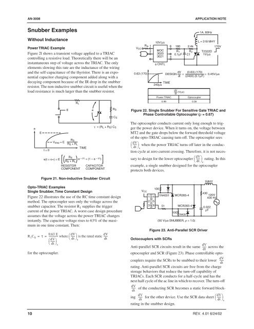
R L<br />
10V/µs<br />
R in 1<br />
6 180 2.4k<br />
V CC<br />
2 MOC R 1 R 2<br />
3020 0.1µF C1<br />
3021 4<br />
0.63 (170)<br />
φ CNTL<br />
DESIGN<br />
dV<br />
dt<br />
APPLICATION NOTE<br />
T2322D<br />
1V/µs<br />
(0.63) (170)<br />
= = 0.45V/µs<br />
(2400) (0.1µF)<br />
TIME<br />
240µs<br />
dV<br />
dt (V/µs)<br />
<strong>Power</strong> TRIAC<br />
Optocoupler<br />
0.99 0.35<br />
1A, 60Hz<br />
L = 318 MHY<br />
170V<br />
E<br />
e<br />
R S<br />
C S<br />
Figure 22. Single <strong>Snubber</strong> For Sensitive Gate TRIAC <strong>and</strong><br />
Phase <strong>Control</strong>lable Optocoupler (ρ = 0.67)<br />
e<br />
E<br />
t = 0<br />
V step = E<br />
R S<br />
R S + R L<br />
TIME<br />
τ = (R L + R S) C S<br />
e(t = o+) = E<br />
R S<br />
R S + R L<br />
e – t/τ + (1 – e – t/τ )<br />
RESISTOR CAPACITOR<br />
COMPONENT COMPONENT<br />
The optocoupler conducts current only long enough to trigger<br />
the power device. When it turns on, the voltage between<br />
MT2 <strong>and</strong> the gate drops below the <strong>for</strong>ward threshold voltage<br />
of the opto-TRIAC causing turn-off. The optocoupler sees<br />
⎛dV<br />
------ ⎞<br />
⎝<br />
when the power TRIAC turns off later in the conduction<br />
cycle at zero current crossing. There<strong>for</strong>e, it is not neces-<br />
dt ⎠s<br />
sary to design <strong>for</strong> the lower optocoupler ⎛dV<br />
------ ⎞<br />
⎝<br />
rating. In this<br />
dt ⎠c<br />
example, a single snubber designed <strong>for</strong> the optocoupler<br />
protects both devices.<br />
Figure 21. Non-inductive <strong>Snubber</strong> Circuit<br />
Opto-TRIAC Examples<br />
Single <strong>Snubber</strong>, Time Constant Design<br />
Figure 22 illustrates the use of the <strong>RC</strong> time constant design<br />
method. The optocoupler sees only the voltage across the<br />
snubber capacitor. The resistor R 1 supplies the trigger<br />
current of the power TRIAC. A worst case design procedure<br />
assumes that the voltage across the power TRIAC changes<br />
instantly. The capacitor voltage rises to 63% of the maximum<br />
in one time constant. Then:<br />
0.63 E dV<br />
R 1 C S = τ = --------------- where ⎛------<br />
⎞ is the rated static dV ------<br />
⎛dV<br />
⎝<br />
------ ⎞ dt ⎠s<br />
dt<br />
⎝ dt ⎠s<br />
<strong>for</strong> the optocoupler.<br />
V CC<br />
1<br />
2<br />
3<br />
MOC3031<br />
4<br />
5<br />
6<br />
100<br />
1N4001<br />
51<br />
MCR265-4<br />
MCR265-4<br />
100<br />
1N4001<br />
(50 V/µs SNUBBER, ρ = 1.0)<br />
0.022<br />
µF<br />
Figure 23. Anti-Parallel SCR Driver<br />
1MHY<br />
430<br />
120V<br />
400 Hz<br />
Octocouplers with SCRs<br />
dV<br />
Anti-parallel SCR circuits result in the same ------ across the<br />
dt<br />
optocoupler <strong>and</strong> SCR (Figure 23). Phase controllable optocouplers<br />
require the SCRs to be snubbed to their lower ------<br />
dV<br />
dt<br />
rating. Anti-parallel SCR circuits are free from the charge<br />
storage behaviors that reduce the turn-off capability of<br />
TRIACs. Each SCR conducts <strong>for</strong> a half-cycle <strong>and</strong> has the<br />
next half cycle of the ac line in which to recover. The turn-off<br />
dV<br />
------ of the conducting SCR becomes a static <strong>for</strong>ward blocking<br />
------ <strong>for</strong> the other device. Use the SCR data sheet ⎛dV<br />
------ ⎞<br />
dt<br />
dV<br />
dt<br />
⎝ dt ⎠s<br />
rating in the snubber design.<br />
10 REV. 4.01 6/24/02


