

AN-3008 RC Snubber Networks for Thyristor Power Control and ...
AN-3008 RC Snubber Networks for Thyristor Power Control and ...
AN-3008 RC Snubber Networks for Thyristor Power Control and ...

Create successful ePaper yourself
Turn your PDF publications into a flip-book with our unique Google optimized e-Paper software.
APPLICATION NOTE<br />
<strong>AN</strong>-<strong>3008</strong><br />
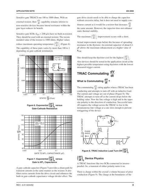
Sensitive gate TRIACS run 100 to 1000 ohms. With an gate drive circuit needs to be able to charge the capacitor<br />
dV<br />
without excessive delay, but it does not need to supply continuous<br />
current as it would <strong>for</strong> a resistor that increases ------<br />
external resistor, their ------ capability remains inferior to<br />
dt<br />
dV<br />
non-sensitive devices because lateral resistance within the<br />
dt<br />
dV<br />
dV<br />
Figure 7. Exponential ( versus<br />
Device Physics<br />
dt<br />
) s<br />
( )<br />
dt c<br />
gate layer reduces its benefit.<br />
the same amount. However, the capacitor does not enhance<br />
static thermal stability.<br />
Sensitive gate SCRs (I GT < 200 µA) have no built-in resistor.<br />
They should be used with an external resistor. The recommended<br />
value of the resistor is 1000 ohms. Higher values<br />
The maximum ⎛dV<br />
------ ⎞<br />
⎝<br />
improvement occurs with a short.<br />
dt ⎠s<br />
reduce maximum operating temperature ⎛dV<br />
Actual improvement stops be<strong>for</strong>e this because of spreading<br />
------ ⎞<br />
⎝<br />
(Figure 6).<br />
dt ⎠<br />
resistance in the thyristor. An external capacitor of about 0.1<br />
s<br />
The capability of these parts varies by more than 100 to 1 µF allows the maximum enhancement at a higher value of<br />
depending on gate-cathode termination.<br />
R GK .<br />
10 MEG<br />
MCR22-2<br />
One should keep the thyristor cool <strong>for</strong> the highest ⎛dV<br />
------ ⎞<br />
⎝<br />
.<br />
T A = 65°C<br />
dt ⎠s<br />
Also devices should be tested in the application circuit at the<br />
A<br />
10<br />
highest possible temperature using thyristors with the lowest<br />
1 MEG<br />
V G<br />
measured trigger current.<br />
K<br />
dV<br />
TRIAC Commutating<br />
dt<br />
100K<br />
dV<br />
What is Commutating ?<br />
dt<br />
dV<br />
The commutating ------ rating applies when a TRIAC has been<br />
dt<br />
conducting <strong>and</strong> attempts to turn-off with an inductive load.<br />
10K<br />
0.001 0.01 0.1 1 10 100 The current <strong>and</strong> voltage are out of phase (Figure 8). The<br />
dV<br />
TRIAC attempts to turn-off as the current drops below the<br />
STATIC (V/µs)<br />
dt<br />
holding value. Now the line voltage is high <strong>and</strong> in the opposite<br />
polarity to the direction of conduction. Successful turnoff<br />
requires the voltage across the TRIAC to rise to the<br />
dV<br />
Figure 6. Exponential ( versus<br />
dt<br />
) s<br />
Gate-Cathode Resistance<br />
instantaneous line voltage at a rate slow enough to prevent<br />
retriggering of the device.<br />
130<br />
R L<br />
120<br />
i 2<br />
V LINE<br />
MAC 228-10<br />
G<br />
V MT2-1<br />
110<br />
800V 110°C<br />
1<br />
dl<br />
100<br />
PHASE<br />
dt c<br />
90<br />
<strong>AN</strong>GLE<br />
φ<br />
80<br />
TIME<br />
TIME<br />
dV<br />
70<br />
i<br />
V LINE<br />
dt c<br />
60<br />
dV<br />
0.001 0.01<br />
0.1 1 Figure 8. TRIAC Inductive Load Turn-Off (<br />
dt<br />
)<br />
GATE TO MT 1, CAPACIT<strong>AN</strong>CE (µF)<br />
c<br />
Gate to MT 1 Capacitance<br />
A TRIAC functions like two SCRs connected in inverseparallel.<br />
So, a transient of either polarity turns it on.<br />
GATE-CATHODE RESIST<strong>AN</strong>CE (OHMS)<br />
dV<br />
STATIC (V/µs)<br />
dt<br />
A gate-cathode capacitor (Figure 7) provides a shunt path <strong>for</strong><br />
transient currents in the same manner as the resistor. It also<br />
filters noise currents from the drive circuit <strong>and</strong> enhances the<br />
built-in gate-cathode capacitance voltage divider effect. The<br />
VOLTAGE CURRENT<br />
There is charge within the crystal’s volume because of prior<br />
conduction (Figure 9). The charge at the boundaries of the<br />
VMT2-1<br />
REV. 4.01 6/24/02 3


