

AN-3008 RC Snubber Networks for Thyristor Power Control and ...
AN-3008 RC Snubber Networks for Thyristor Power Control and ...
AN-3008 RC Snubber Networks for Thyristor Power Control and ...

You also want an ePaper? Increase the reach of your titles
YUMPU automatically turns print PDFs into web optimized ePapers that Google loves.
APPLICATION NOTE<br />
<strong>AN</strong>-<strong>3008</strong><br />
1.8<br />
I ER<br />
ξ = ------ – ---------- L<br />
C S L<br />
⎛dV<br />
------ ⎞ = initial instantaneous dV ------ at t = 0, ignoring any instantaneous voltage step at<br />
⎝ dt ⎠0<br />
dt<br />
t = 0 because of I RRM<br />
1.9<br />
⎛dV<br />
------ ⎞<br />
⎝ dt ⎠0<br />
=<br />
R T<br />
V OL ------ + ξ. For All Damping Conditions<br />
L<br />
2.0<br />
When I = 0,<br />
⎛ dV ------ ⎞ =<br />
⎝ dt ⎠0<br />
ER<br />
---------- S<br />
L<br />
⎛dV<br />
------ ⎞ =<br />
⎝ dt ⎠max<br />
t max =<br />
Maximum Instantaneous dV ------<br />
dt<br />
Time of maximum instantaneous dV ------<br />
dt<br />
t peak = Time of maximum instantaneous peak voltage across thyristor<br />
Average dV ------ = V<br />
dt PK ⁄ t PK = Slope of the secant line from t = 0 through V PK<br />
V PK<br />
=<br />
Maximum instantaneous voltage across the thyristor.<br />
Constants (depending on the damping factor):<br />
2.1<br />
No Damping ( ρ = 0 )<br />
ω = ω 0<br />
R T = α = ρ = 0<br />
2.2<br />
Underdamped ( 0 < ρ < 1)<br />
ω = ω0 2 – α 2 = ω0 1–<br />
ρ 2<br />
2.3<br />
Critial Damped ( ρ = 1)<br />
α<br />
ω0, ω 0R , 2 L C --- , C 2<br />
= = = = ----------<br />
αR T<br />
2.4<br />
Overdamped ( ρ > 1)<br />
ω = α 2 – ω0 2 = ω0 ρ 2 – 1<br />
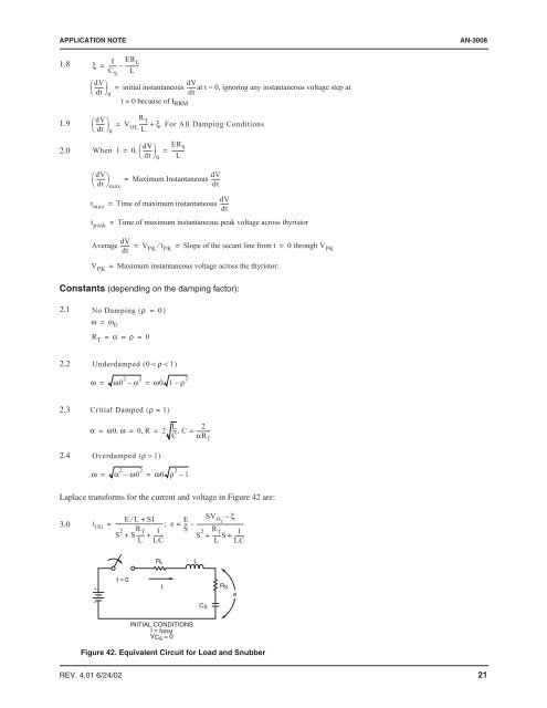
Laplace trans<strong>for</strong>ms <strong>for</strong> the current <strong>and</strong> voltage in Figure 42 are:<br />
3.0<br />
E⁄<br />
L+<br />
SI E<br />
SV OL<br />
– ξ<br />
i ( S)<br />
= -------------------------------------<br />
S 2 S R ; e = -- – -------------------------------------<br />
T 1 S<br />
+ ------ + ------- S 2 R T 1<br />
+ ------S + -------<br />
L LC<br />
L LC<br />
R L<br />
L<br />
+<br />
–<br />
t = 0<br />
I<br />
C S<br />
R S<br />
e<br />
INITIAL CONDITIONS<br />
I = I RRM<br />
VC S = 0<br />
Figure 42. Equivalent Circuit <strong>for</strong> Load <strong>and</strong> <strong>Snubber</strong><br />
REV. 4.01 6/24/02 21


