

AN-3008 RC Snubber Networks for Thyristor Power Control and ...
AN-3008 RC Snubber Networks for Thyristor Power Control and ...
AN-3008 RC Snubber Networks for Thyristor Power Control and ...

Create successful ePaper yourself
Turn your PDF publications into a flip-book with our unique Google optimized e-Paper software.
APPLICATION NOTE<br />
<strong>AN</strong>-<strong>3008</strong><br />
100 µH<br />
20A<br />
LS1<br />
10 0.33 µF<br />
< 50 V/µs<br />
MAC 218-6<br />
8A LOAD<br />
R<br />
68Ω<br />
0.033 µF<br />
L<br />
120V<br />
60Hz<br />
340<br />
V<br />
12Ω<br />
HEATER<br />
dV<br />
dt<br />
s<br />
= 100 V/µs<br />
dV<br />
= 5 V/µs<br />
dt c<br />
Figure 27. Snubbing <strong>for</strong> a Resistive Load<br />
Given E = 240 2 = 340V<br />
Pick ρ = 0.3<br />
Then from Figure 18, V PK = 1.42 (340) = 483 V.<br />
Thus, it will be necessary to use a 600 V device. Using the<br />
previously stated <strong>for</strong>mulas <strong>for</strong> ω 0 , C <strong>and</strong> R we find:<br />
5 0× 10 6 V/S<br />
ω 0 = ---------------------------------- = 201450 rps<br />
( 0.73) ( 340 V)<br />
1<br />
C = --------------------------------------------------------<br />
( 201450) 2 ( 100 × 10 – 6 = 0.2464µF<br />
)<br />
100 × 10 – 6<br />
R = 2( 0.3)<br />
--------------------------------- 0.2464 × 10 – 6 = 12ohms<br />
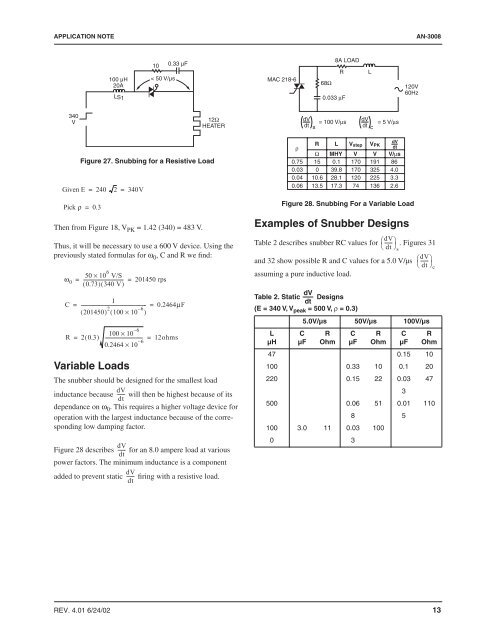
Variable Loads<br />
The snubber should be designed <strong>for</strong> the smallest load<br />
dV<br />
inductance because ------ will then be highest because of its<br />
dt<br />
dependance on ω 0 . This requires a higher voltage device <strong>for</strong><br />
operation with the largest inductance because of the corresponding<br />
low damping factor.<br />
dV<br />
Figure 28 describes ------ <strong>for</strong> an 8.0 ampere load at various<br />
dt<br />
power factors. The minimum inductance is a component<br />
dV<br />
added to prevent static ------ firing with a resistive load.<br />
dt<br />
Figure 28. Snubbing For a Variable Load<br />
Examples of <strong>Snubber</strong> Designs<br />
Table 2 describes snubber <strong>RC</strong> values <strong>for</strong> ⎛dV<br />
------ ⎞<br />
⎝<br />
. Figures 31<br />
dt ⎠s<br />
<strong>and</strong> 32 show possible R <strong>and</strong> C values <strong>for</strong> a 5.0 V/µs ⎛dV<br />
------ ⎞<br />
⎝ dt ⎠c<br />
assuming a pure inductive load.<br />
dV<br />
Table 2. Static Designs<br />
dt<br />
(E = 340 V, V peak = 500 V, ρ = 0.3)<br />
L<br />
µH<br />
dV<br />
R L V step V PK<br />
ρ<br />
dt<br />
Ω MHY V V V/µs<br />
0.75 15 0.1 170 191 86<br />
0.03 0 39.8 170 325 4.0<br />
0.04 10.6 28.1 120 225 3.3<br />
0.06 13.5 17.3 74 136 2.6<br />
C<br />
µF<br />
5.0V/µs 50V/µs 100V/µs<br />
R<br />
Ohm<br />
C<br />
µF<br />
R<br />
Ohm<br />
C<br />
µF<br />
R<br />
Ohm<br />
47 0.15 10<br />
100 0.33 10 0.1 20<br />
220 0.15 22 0.03 47<br />
3<br />
500 0.06 51 0.01 110<br />
8 5<br />
100 3.0 11 0.03 100<br />
0 3<br />
REV. 4.01 6/24/02 13


