

AN-3008 RC Snubber Networks for Thyristor Power Control and ...
AN-3008 RC Snubber Networks for Thyristor Power Control and ...
AN-3008 RC Snubber Networks for Thyristor Power Control and ...

Create successful ePaper yourself
Turn your PDF publications into a flip-book with our unique Google optimized e-Paper software.
APPLICATION NOTE<br />
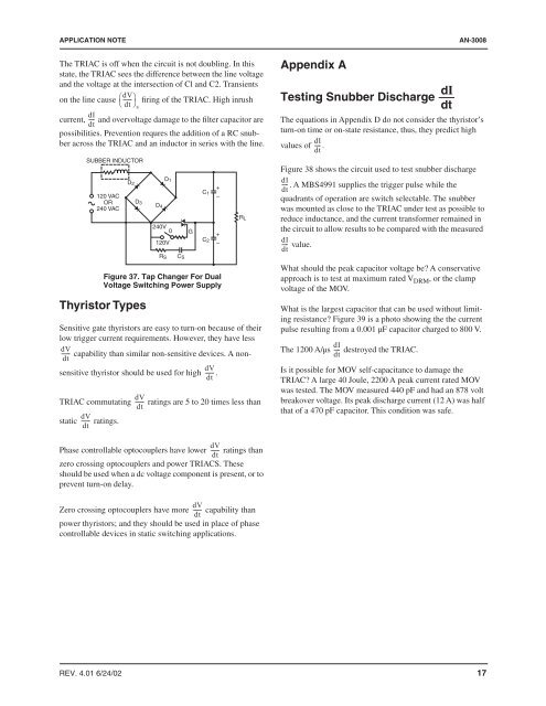
The TRIAC is off when the circuit is not doubling. In this<br />
state, the TRIAC sees the difference between the line voltage<br />
<strong>and</strong> the voltage at the intersection of Cl <strong>and</strong> C2. Transients<br />
on the line cause ⎛dV<br />
------ ⎞<br />
⎝<br />
firing of the TRIAC. High inrush<br />
dt ⎠s<br />
dI<br />
current, ---- <strong>and</strong> overvoltage damage to the filter capacitor are<br />
dt<br />
possibilities. Prevention requres the addition of a <strong>RC</strong> snubber<br />
across the TRIAC <strong>and</strong> an inductor in series with the line.<br />
Figure 37. Tap Changer For Dual<br />
Voltage Switching <strong>Power</strong> Supply<br />
<strong>Thyristor</strong> Types<br />
Sensitive gate thyristors are easy to turn-on because of their<br />
low trigger current requirements. However, they have less<br />
dV<br />
------ capability than similar non-sensitive devices. A nonsensitive<br />
thyristor should be used <strong>for</strong> high ------ .<br />
dt<br />
dV<br />
dt<br />
TRIAC commutating<br />
static<br />
dV<br />
------<br />
dt<br />
SUBBER INDUCTOR<br />
120 VAC<br />
OR<br />
240 VAC<br />
ratings.<br />
D<br />
D 1<br />
2<br />
+<br />
C 1<br />
–<br />
D 3<br />
D 4<br />
240V<br />
0<br />
+<br />
C<br />
120V<br />
2<br />
–<br />
dV<br />
------<br />
dt<br />
R S C S<br />
G<br />
R L<br />
ratings are 5 to 20 times less than<br />
Appendix A<br />
Testing <strong>Snubber</strong> Discharge<br />
dI<br />
dt<br />
<strong>AN</strong>-<strong>3008</strong><br />
The equations in Appendix D do not consider the thyristor’s<br />
turn-on time or on-state resistance, thus, they predict high<br />
dI<br />
values of ---- .<br />
dt<br />
Figure 38 shows the circuit used to test snubber discharge<br />
dI<br />
---- . A MBS4991 supplies the trigger pulse while the<br />
dt<br />
quadrants of operation are switch selectable. The snubber<br />
was mounted as close to the TRIAC under test as possible to<br />
reduce inductance, <strong>and</strong> the current trans<strong>for</strong>mer remained in<br />
the circuit to allow results to be compared with the measured<br />
dI<br />
---- value.<br />
dt<br />
What should the peak capacitor voltage be? A conservative<br />
approach is to test at maximum rated V DRM , or the clamp<br />
voltage of the MOV.<br />
What is the largest capacitor that can be used without limiting<br />
resistance? Figure 39 is a photo showing the the current<br />
pulse resulting from a 0.001 µF capacitor charged to 800 V.<br />
dI<br />
The 1200 A/µs ---- destroyed the TRIAC.<br />
dt<br />
Is it possible <strong>for</strong> MOV self-capacitance to damage the<br />
TRIAC? A large 40 Joule, 2200 A peak current rated MOV<br />
was tested. The MOV measured 440 pF <strong>and</strong> had an 878 volt<br />
breakover voltage. Its peak discharge current (12 A) was half<br />
that of a 470 pF capacitor. This condition was safe.<br />
dV<br />
Phase controllable optocouplers have lower ------ ratings than<br />
dt<br />
zero crossing optocouplers <strong>and</strong> power TRIACS. These<br />
should be used when a dc voltage component is present, or to<br />
prevent turn-on delay.<br />
dV<br />
Zero crossing optocouplers have more ------ capability than<br />
dt<br />
power thyristors; <strong>and</strong> they should be used in place of phase<br />
controllable devices in static switching applications.<br />
REV. 4.01 6/24/02 17


