

AN-9732 - Fairchild Semiconductor
AN-9732 - Fairchild Semiconductor
AN-9732 - Fairchild Semiconductor

You also want an ePaper? Increase the reach of your titles
YUMPU automatically turns print PDFs into web optimized ePapers that Google loves.
<strong>AN</strong>-<strong>9732</strong><br />
www.fairchildsemi.com<br />
LED Application Design Guide Using BCM Power Factor<br />
Correction (PFC) Controller for 200W Lighting System<br />
1. Introduction<br />
This application note presents practical step-by-step design<br />
considerations for a Boundary-Conduction-Mode (BCM)<br />
Power-Factor-Correction (PFC) converter employing<br />
<strong>Fairchild</strong> PFC controller, FL7930. It includes designing the<br />
inductor and Zero-Current-Detection (ZCD) circuit,<br />
selecting the components, and closing the control loop. The<br />
design procedure is verified through an experimental 200W<br />
prototype converter.<br />
Unlike the Continuous Conduction Mode (CCM) technique<br />
often used at this power level, BCM offers inherent zerocurrent<br />
switching of the boost diodes (no reverse-recovery<br />
losses), which permits the use of less expensive diodes<br />
without sacrificing efficiency.<br />
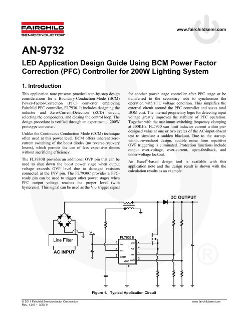
The FL3930B provides an additional OVP pin that can be<br />
used to shut down the boost power stage when output<br />
voltage exceeds OVP level due to damaged resistors<br />
connected at the INV pin. The FL7930C provides a PFCready<br />
pin can be used to trigger other power stages when<br />
PFC output voltage reaches the proper level (with<br />
hysteresis). This signal can be used as the VCC trigger signal<br />
Figure 1. Typical Application Circuit<br />
for another power stage controller after PFC stage or be<br />
transferred to the secondary side to synchronize the<br />
operation with PFC voltage condition. This simplifies the<br />
external circuit around the PFC controller and saves total<br />
BOM cost. The internal proprietary logic for detecting input<br />
voltage greatly improves the stability of PFC operation.<br />
Together with the maximum switching frequency clamping<br />
at 300KHz. FL7930 can limit inductor current within predesigned<br />
value at one or two cycles of the AC-input-absent<br />
test to simulate a sudden blackout. Due to the startupwithout-overshoot<br />
design, audible noise from repetitive<br />
OVP triggering is eliminated. Protection functions include<br />
output over-voltage, over-current, open-feedback, and<br />
under-voltage lockout.<br />
An Excel ® -based design tool is available with this<br />
application note and the design result is shown with the<br />
calculation results as an example.<br />
© 2011 <strong>Fairchild</strong> <strong>Semiconductor</strong> Corporation www.fairchildsemi.com<br />
Rev. 1.0.0 • 3/23/11
<strong>AN</strong>-<strong>9732</strong> APPLICATION NOTE<br />
2. Operation Principle of BCM Boost PFC Converter<br />
The most widely used operation modes for the boost<br />
converter are Continuous Conduction Mode (CCM) and<br />
Boundary Conduction Mode (BCM). These two descriptive<br />
names refer to the current flowing through the energy<br />
storage inductor of the boost converter, as depicted in<br />
Figure 2. As the names indicate, the inductor current in<br />
CCM is continuous; while in BCM, the new switching<br />
period is initiated when the inductor current returns to zero,<br />
which is at the boundary of continuous conduction and<br />
discontinuous conduction operations. Even though the BCM<br />
operation has higher RMS current in the inductor and<br />
switching devices, it allows better switching condition for<br />
the MOSFET and the diode. As shown in Figure 2, the<br />
diode reverse recovery is eliminated and a fast-recovery<br />
diode is not needed. The MOSFET is also turned on with<br />
zero current, which reduces the switching loss.<br />
Figure 2. CCM vs. BCM Control<br />
The fundamental idea of BCM PFC is that the inductor<br />
current starts from zero in each switching period, as shown<br />
in Figure 3. When the power transistor of the boost<br />
converter is turned on for a fixed time, the peak inductor<br />
current is proportional to the input voltage. Since the current<br />
waveform is triangular; the average value in each switching<br />
period is proportional to the input voltage. In a sinusoidal<br />
input voltage, the input current of the converter follows the<br />
input voltage waveform with very high accuracy and draws<br />
a sinusoidal input current from the source. This behavior<br />
makes the boost converter in BCM operation an ideal<br />
candidate for power factor correction.<br />
A by-product of BCM is that the boost converter runs with<br />
variable switching frequency that depends primarily on the<br />
selected output voltage, the instantaneous value of the input<br />
voltage, the boost inductor value, and the output power<br />
delivered to the load. The operating frequency changes as<br />
the input current follows the sinusoidal input voltage<br />
waveform, as shown in Figure 3. The lowest frequency<br />
occurs at the peak of sinusoidal line voltage.<br />
Figure 3. Operation Waveforms of BCM PFC<br />
The voltage-second balance equation for the inductor is:<br />
VOUT VIN<br />
( t ) tOFF<br />
V ( t ) t <br />
<br />
(1)<br />
© 2011 <strong>Fairchild</strong> <strong>Semiconductor</strong> Corporation www.fairchildsemi.com<br />
Rev. 1.0.0 • 3/23/11 2<br />
IN<br />
ON<br />
where VIN(t) is the rectified line voltage and VOUT is the<br />
output voltage.<br />
The switching frequency of BCM boost PFC converter is:<br />
f<br />
SW<br />
1<br />
<br />
tON<br />
t<br />
1 V<br />
<br />
t<br />
ON<br />
OFF<br />
OUT<br />
<br />
V<br />
1<br />
t<br />
ON<br />
IN,<br />
PK<br />
V<br />
<br />
V<br />
OUT<br />
sin<br />
OUT<br />
V<br />
V<br />
OUT<br />
IN<br />
( t )<br />
2ft LINE<br />
where VIN,PK is the amplitude of the line voltage and fLINE is<br />
the line frequency.<br />
Figure 4 shows how the MOSFET on time and switching<br />
frequency changes as output power decreases. When the<br />
load decreases, as shown in the right side of Figure 4, the<br />
peak inductor current diminishes with reduced MOSFET on<br />
time and, therefore, the switching frequency increases.<br />
Since this can cause severe switching losses at light-load<br />
condition and too-high switching frequency operation may<br />
occur at startup, the maximum switching frequency of<br />
FL7930 is limited to 300KHz.<br />
(2)
<strong>AN</strong>-<strong>9732</strong> APPLICATION NOTE<br />
Figure 4. Frequency Variation of BCM PFC<br />
Since the design of the filter and inductor for a BCM PFC<br />
converter with variable switching frequency should be at<br />
minimum frequency condition, it is worthwhile to examine<br />
how the minimum frequency of BCM PFC converter<br />
changes with operating conditions.<br />
Figure 5 shows the minimum switching frequency, which<br />
occurs at the peak of line voltage as a function of the RMS<br />
line voltage for three output voltage settings. It is interesting<br />
that, depending on where the output voltage is set, the<br />
minimum switching frequency may occur at the minimum<br />
or at the maximum line voltage. When the output voltage is<br />
approximately 405V, the minimum switching frequency is<br />
the same for both low line (85VAC) and high line (265VAC).<br />
Minimum Switching Frequency[KHz]<br />
150<br />
140<br />
130<br />
120<br />
110<br />
100<br />
90<br />
80<br />
70<br />
60<br />
50<br />
40<br />
30<br />
20<br />
10<br />
Vout=385V<br />
Vout=400V<br />
Vout=415V<br />
85 130 175 220 265<br />
Line Voltage [V]<br />
Figure 5. Minimum Switching Frequency vs. RMS Line<br />
Voltage (L = 200µH, POUT = 200W)<br />
3. Startup without Overshoot and<br />
AC-Absent Detection<br />
Because feedback control speed of the PFC is typically quite<br />
slow, there is a gap between output voltage and feedback<br />
control. Therefore, Over-Voltage Protection (OVP) is<br />
critical at the PFC controller. Voltage dip caused by fast<br />
load change from light to heavy is diminished by a large<br />
bulk capacitor. OVP is easily triggered at startup. Switching<br />
starting and stopping by OVP at startup may cause audible<br />
noise and can increase voltage stress at startup, which may<br />
be higher than normal operation. This is improved if softstart<br />
time is very long, but too-long start time raises the time<br />
needed for the output voltage to reach the rated value at<br />
light load. FL7930 includes a startup without overshoot<br />
feature. During startup, the feedback loop is controlled by<br />
an internal proportional gain controller and, when the output<br />
voltage reaches the vicinity of the rated value, changed to<br />
the external compensator after an internally fixed transition<br />
time described in the Figure 6. In short, an internal<br />
proportional gain controller prevents overshoot at startup;<br />
external conventional compensator takes over after startup.<br />
Figure 6. Startup Without Overshoot<br />
FL7930 eliminates AC input voltage detection to save the<br />
power loss caused by an input-voltage-sensing resistor array<br />
and to optimize THD. Therefore, no information about input<br />
voltage is available at the internal controller. In many cases,<br />
the VCC of PFC controller is supplied by an independent<br />
power source, like standby power, so when the electric<br />
power is suddenly interrupted during one or two AC line<br />
periods, VCC is still alive during that time and PFC output<br />
voltage drops. Accordingly, the control loop tries to<br />
compensate output voltage drop and control voltage reaches<br />
its maximum. When AC line input voltage is live, control<br />
voltage allows high switching current and creates stress on<br />
the MOSFET and diode. To protect against this, FL7930<br />
checks if the input AC voltage exists. Once controller<br />
verifies that the input voltage does not exist, soft-start is<br />
reset and waits until AC input voltage is applied again. Softstart<br />
manages the turn-on time for smooth operation after<br />
detecting that the AC voltage is live and results in less<br />
voltage and current stress during startup.<br />
© 2011 <strong>Fairchild</strong> <strong>Semiconductor</strong> Corporation www.fairchildsemi.com<br />
Rev. 1.0.0 • 3/23/11 3
<strong>AN</strong>-<strong>9732</strong> APPLICATION NOTE<br />
Figure 7. AC-Off Operation without AC-Absent<br />
Detection Circuit<br />
4. Design Considerations<br />
In this section, a design procedure is presented using the<br />
schematic in Figure 9 as a reference. A 200W PFC<br />
application with universal input range is selected as a design<br />
example. The design specifications are:<br />
Line Voltage Range: 90~265VAC (Universal Input), 50Hz<br />
Nominal Output Voltage and Current: 400V/0.5A (200W)<br />
Figure 8. AC-Off Operation with AC-Absent<br />
Detection Circuit<br />
Hold-up Time Requirement: Output Voltage Should Not<br />
Drop Below 330V During One Line Cycle<br />
Output Voltage Ripple: Less than 8VPP<br />
Minimum Switching Frequency: Higher than 50kHz<br />
Control Bandwidth: 5~15Hz<br />
VCC supplied from auxiliary power supply.<br />
Figure 9. Reference Circuit for Design Example of BCM Boost PFC<br />
© 2011 <strong>Fairchild</strong> <strong>Semiconductor</strong> Corporation www.fairchildsemi.com<br />
Rev. 1.0.0 • 3/23/11 4
<strong>AN</strong>-<strong>9732</strong> APPLICATION NOTE<br />
[STEP-1] Define System Specifications<br />
Line Frequency Range (VLINE,MIN and VLINE,MAX)<br />
Line Frequency (fLINE)<br />
Output-Voltage (VOUT)<br />
Output Load Current (IOUT)<br />
Output Power (POUT =VOUT IOUT)<br />
Estimated Efficiency ()<br />
To calculate the maximum input power, it is necessary to<br />
estimate the power conversion efficiency. At universal input<br />
range, efficiency is recommended at 0.9; 0.93~0.95 is<br />
recommended when input voltage is high.<br />
When input voltage is set at the minimum, input current<br />
becomes the maximum to deliver the same power compared<br />
at high line. Maximum boost inductor current can be<br />
detected at the minimum line voltage and at its peak.<br />
Inductor current can be divided into two categories; one is<br />
rising current when MOSFET is on and the other is output<br />
diode current when MOSFET is off, as shown in Figure 10.<br />
Figure 10. Inductor and Input Current<br />
Because switching frequency is much higher than line<br />
frequency, input current can be assumed to be constant<br />
during a switching period, as shown in Figure 11.<br />
Figure 11. Inductor and Input Current<br />
With the estimated efficiency, Figure 10 and Figure 11<br />
inductor current peak (IL,PK), maximum input current<br />
(IIN,MAX), and input Root Mean Square (RMS) current<br />
(IIN,MAXRMS) are given as:<br />
I<br />
L , PK<br />
<br />
<br />
I PK<br />
4 P<br />
2 V<br />
OUT<br />
LINE<br />
, MIN<br />
[ A ]<br />
IN, MAX IL,<br />
/ 2 [ A]<br />
(4)<br />
I MAX<br />
IN, MAXRMS IIN,<br />
/ 2 [ A]<br />
(5)<br />
(3)<br />
(Design Example) Input voltage range is universal input,<br />
output load is 500mA, and estimated efficiency is selected<br />
as 0.9.<br />
VLINE,<br />
MIN 90 VAC<br />
, VLINE,<br />
MAX 265V<br />
AC<br />
f LINE 50Hz<br />
VOUT<br />
400V<br />
, IOUT<br />
500mA<br />
0.<br />
9<br />
I L,<br />
PK <br />
<br />
4<br />
POUT<br />
2 VLINE,<br />
MIN<br />
4<br />
400V<br />
0.<br />
5A<br />
<br />
6.<br />
984A<br />
0.<br />
9<br />
2 90<br />
I L,<br />
PK<br />
I IN,<br />
MAX <br />
2<br />
6.<br />
984A<br />
3.<br />
492A<br />
2<br />
I IN,<br />
MAX<br />
I IN,<br />
MAXRMS <br />
2<br />
3.<br />
492A<br />
2.<br />
469A<br />
2<br />
[STEP-2] Boost Inductor Design<br />
The boost inductor value is determined by the output power<br />
and the minimum switching frequency. The minimum<br />
switching frequency must be higher than the maximum<br />
audible frequency band of 20kHz. Minimum frequency near<br />
20kHz can decrease switching loss with the cost of<br />
increased inductor size and line filter size. Too-high<br />
minimum frequency may increase the switching loss and<br />
make the system respond to noise. Selecting in the range of<br />
about 30~60kHz is a common choice; 40~50kHz is<br />
recommended with FL7930.<br />
The minimum switching frequency may appear at minimum<br />
input voltage or maximum input voltage, depending on the<br />
output voltage level. When PFC output voltage is less than<br />
405V, minimum switching appears at the maximum input<br />
voltage, according to application note <strong>AN</strong>-6086. Inductance<br />
is obtained using the minimum switching frequency:<br />
2 2VLINE<br />
[ H ]<br />
<br />
L <br />
2V<br />
<br />
LINE<br />
4 fSW<br />
, MIN POUT<br />
1<br />
<br />
<br />
VOUT<br />
2V<br />
<br />
LINE <br />
where L is boost inductance and fSW,MIN is the minimum<br />
switching frequency.<br />
© 2011 <strong>Fairchild</strong> <strong>Semiconductor</strong> Corporation www.fairchildsemi.com<br />
Rev. 1.0.0 • 3/23/11 5<br />
(6)
<strong>AN</strong>-<strong>9732</strong> APPLICATION NOTE<br />
The maximum on time needed to carry peak inductor<br />
current is calculated as:<br />
IL,<br />
PK<br />
tON,<br />
MAX L <br />
2 VLINE,<br />
MIN<br />
[s]<br />
Once inductance and the maximum inductor current are<br />
calculated, the number of turns of the boost inductor should<br />
be determined considering the core saturation. The<br />
minimum number of turns is given as:<br />
N<br />
BOOST<br />
(7)<br />
IL,<br />
PK L[<br />
H<br />
]<br />
[ Turns ]<br />
2<br />
(8)<br />
A [ mm ] B<br />
e<br />
where Ae is the cross-sectional area of core and B is the<br />
maximum flux swing of the core in Tesla. B should be set<br />
below the saturation flux density.<br />
Figure 12 shows the typical B-H characteristics of ferrite<br />
core from TDK (PC45). Since the saturation flux density<br />
(B) decreases as the temperature increases, the high<br />
temperature characteristics should be considered.<br />
RMS inductor current (IL,RMS) and current density of the coil<br />
(IL,DENSITY) can be given as:<br />
IL,<br />
PK<br />
IL,<br />
RMS [ A]<br />
(9)<br />
6<br />
I<br />
L,<br />
DENSITY<br />
IL,<br />
RMS<br />
2<br />
<br />
[ A / mm ]<br />
2<br />
d<br />
<br />
wire <br />
N<br />
(10)<br />
2 wire<br />
<br />
where dWIRE is the diameter of winding wire and NWIRE is<br />
the number of strands of winding wire.<br />
When selecting wire diameter and strands; current density,<br />
window area (AW, refer to Figure 13) of selected core, and<br />
fill factor need to be considered. Winding sequence of the<br />
boost inductor is relatively simple compared to a DC-DC<br />
converter, so fill factor can be assumed about 0.2~0.3.<br />
Layers cause the skin effect and proximity effect in the coil,<br />
so real current density may be higher than expected.<br />
Figure 12. Typical B-H Curves of Ferrite Core<br />
Figure 13. Ae and AW<br />
(Design Example) Since the output voltage is 400V, the<br />
minimum frequency occurs at high-line (265VAC) and fullload<br />
condition. Assuming the efficiency is 90% and<br />
selecting the minimum frequency as 50kHz, the inductor<br />
value is obtained as:<br />
2<br />
<br />
2VLINE<br />
<br />
L <br />
2V<br />
<br />
LINE<br />
4<br />
f SW,<br />
MIN POUT<br />
1<br />
<br />
V 2V<br />
<br />
OUT LINE <br />
2<br />
0.<br />
9<br />
2 265<br />
<br />
199.<br />
4[<br />
H<br />
]<br />
<br />
3<br />
2 265 <br />
4 50 10 200 <br />
<br />
1<br />
<br />
<br />
400 2 265<br />
<br />
<br />
Assuming EER3019N core (PL-7, Ae=137mm 2 ) is used<br />
and setting B as 0.3T, the primary winding should be:<br />
I L,<br />
PK L[<br />
H<br />
] 6.<br />
984 284<br />
N BOOST <br />
<br />
34[<br />
T ]<br />
2<br />
A [ mm ] B<br />
137 0.<br />
3<br />
© 2011 <strong>Fairchild</strong> <strong>Semiconductor</strong> Corporation www.fairchildsemi.com<br />
Rev. 1.0.0 • 3/23/11 6<br />
e<br />
The number of turns (NBOOST) of the boost inductor is<br />
determined as 34 turns.<br />
When 0.10mm diameter and 50-strand wire is used, RMS<br />
current of inductor coil and current density are:<br />
IL,<br />
PK 6.<br />
984<br />
I L,<br />
RMS 2.<br />
85[<br />
A]<br />
6 6<br />
I L,<br />
RMS<br />
I L,<br />
DENSITY <br />
<br />
2<br />
d<br />
wire <br />
<br />
<br />
N<br />
2 wire<br />
<br />
2.<br />
85<br />
2<br />
7.<br />
3 [ A/<br />
mm ]<br />
2<br />
50<br />
0. 1/<br />
2
<strong>AN</strong>-<strong>9732</strong> APPLICATION NOTE<br />
[STEP-3] Inductor Auxiliary Winding Design<br />
Figure 14 shows the application circuit of nearby ZCD pin<br />
from auxiliary winding.<br />
Figure 14. Application Circuit of ZCD Pin<br />
The first role of ZCD winding is detecting the zero-current<br />
point of the boost inductor. Once the boost inductor current<br />
becomes zero, the effective capacitor shown at the<br />
MOSFET drain pin (Ceff) and the boost inductor resonate<br />
together. To minimize the constant turn-on time<br />
deterioration and turn-on loss, the gate is turned on again<br />
when the drain source voltage of the MOSFET (VDS)<br />
reaches the valley point shown in Figure 15. When input<br />
voltage is lower than half of the boosted output voltage,<br />
Zero Voltage Switching (ZVS) is possible if MOSFET turnon<br />
is triggered at valley point.<br />
Figure 15. ZCD Detection Waveforms<br />
Auxiliary winding must give enough energy to trigger ZCD<br />
threshold to detect zero current. Minimum auxiliary winding<br />
turns are given as:<br />
1.<br />
5V<br />
NBOOST<br />
[ Turns]<br />
(11)<br />
V 2V<br />
© 2011 <strong>Fairchild</strong> <strong>Semiconductor</strong> Corporation www.fairchildsemi.com<br />
Rev. 1.0.0 • 3/23/11 7<br />
N<br />
AUX<br />
OUT<br />
LINE,<br />
MAX<br />
where 1.5V is the positive threshold of the ZCD pin.<br />
To guarantee stable operation, auxiliary winding turns are<br />
recommended to add 2~3 turns to the calculation result of<br />
Equation (11). However, too many auxiliary winding turns<br />
raise the negative clamping loss at high line and positive<br />
clamping loss at low line.<br />
(Design Example) 34 turns are selected as boost inductor<br />
turns and auxiliary winding turns are calculated as:<br />
N<br />
AUX<br />
1.<br />
5V<br />
N<br />
<br />
V 2V<br />
OUT<br />
BOOST<br />
LINE,<br />
MAX<br />
1.<br />
5 34<br />
<br />
2.<br />
02[<br />
Turns]<br />
400<br />
2 265<br />
Choice should be around 4~5 turns after adding 2~3 turns.<br />
[STEP-4] ZCD Circuit Design<br />
If a transition time when VAUXILIARY drops from 1.4V to 0V<br />
is ignored from Figure 15, the needed additional delay by<br />
the external resistor and capacitor is one quarter of the<br />
resonant period. The time constant made by ZCD resistor<br />
and capacitor should be the same as one quarter of the<br />
resonant period:<br />
2<br />
Ceff<br />
L<br />
RZCD<br />
CZCD<br />
<br />
(12)<br />
4<br />
where Ceff is the effective capacitor shown at the MOSFET<br />
drain pin; CZCD is the external capacitance at the ZCD pin;<br />
and RZCD is the external resistance at the ZCD pin.<br />
The second role of RZCD is the current limit of the internal<br />
negative clamp circuit when auxiliary voltage drops to<br />
negative due to MOSFET turn on. ZCD voltage is clamped<br />
0.65V and minimum RZCD can be given as:<br />
R<br />
ZCD<br />
N<br />
<br />
<br />
N<br />
<br />
AUX<br />
BOOST<br />
2V<br />
LINE,<br />
MAX<br />
3mA<br />
<br />
0.<br />
65V<br />
<br />
<br />
<br />
[ ]<br />
where 3mA is the clamping capability of the ZCD pin.<br />
(13)<br />
The calculation result of Equation (13) is normally higher<br />
than 15k. If 20k is assumed as RZCD, calculated CZCD<br />
from Equation (12) is around 10pF when the other<br />
components are assumed as conventional values used in the
<strong>AN</strong>-<strong>9732</strong> APPLICATION NOTE<br />
field. Because most IC pins have several pF parasitic<br />
capacitance, CZCD can be eliminated when RZCD is higher<br />
than 30k. However, a small capacitor would be helpful<br />
when auxiliary winding suffers from operating noise.<br />
The PFC control loop has two conflicting goals: output<br />
voltage regulation and making the input current shape the<br />
same as input voltage. If the control loop reacts to regulate<br />
output voltage smoothly, as shown in Figure 16, control<br />
voltage varies widely with the input voltage variation. Input<br />
current acts to the control loop and sinusoidal input current<br />
shape cannot be attained. This is the reason control response<br />
of most PFC topologies is very slow and turn-on time over<br />
AC period is kept constant. This is also the reason output<br />
voltage ripple is made by input and output power<br />
relationship, not by control-loop performance.<br />
VIN & VOUT<br />
VCONTROL<br />
IACIN<br />
Figure 16. Input Current Deterioration by Fast Control<br />
If on-time is controlled constantly over one AC period,<br />
inductor current peak follows AC input voltage shape and<br />
achieves good power factor. Off-time is basically inductor<br />
current reset time due to the boundary mode and is<br />
determined by the input and output voltage difference.<br />
When input voltage is at its peak, the voltage difference<br />
between input and output voltage is small, and long turn-off<br />
time is necessary. When input voltage is near zero, turn-off<br />
time is short, as shown in Figure 17 and Figure 18. Though<br />
inductor current drops to zero, there is a minor delay,<br />
explained above. The delay can be assumed as fixed when<br />
AC is at line peak and zero. Near AC line peak, the inductor<br />
current decreasing slope is slow and inductor current slope<br />
is also slow during the ZCD delay. The amount of negative<br />
current is not much higher than the inductor current peak.<br />
Near the AC line zero, inductor current decreasing slope is<br />
very high and the amount of negative current is higher than<br />
positive inductor current peak because input voltage is<br />
almost zero.<br />
t<br />
Figure 17. Inductor Current at AC Voltage Peak<br />
Figure 18. Inductor Current at AC Voltage Zero<br />
Negative inductor current creates zero current distortion and<br />
degrades the power factor. Improve this by extending turnon<br />
time at the AC line input near the zero cross.<br />
Negative auxiliary winding voltage, when MOSFET is<br />
turned on, is linearly proportional to the input voltage.<br />
Sourcing current generated by the internal negative<br />
clamping circuit is also proportional to sinusoidal input<br />
voltage. That current is detected internally and added to the<br />
internal sawtooth generator, as shown in Figure 19.<br />
© 2011 <strong>Fairchild</strong> <strong>Semiconductor</strong> Corporation www.fairchildsemi.com<br />
Rev. 1.0.0 • 3/23/11 8
<strong>AN</strong>-<strong>9732</strong> APPLICATION NOTE<br />
Figure 19. ZCD Current and Sawtooth Generator<br />
When AC input voltage is almost zero, no negative current<br />
is generated from inside, but sourcing current when input<br />
voltage is high is used to raise the sawtooth generator slope<br />
and turn-on time is shorter. As a result, turn-on time when<br />
AC voltage is zero is longer compared to AC voltage, in<br />
peaks shown in Figure 20.<br />
Figure 20. THD Improvement<br />
The current that comes from the ZCD pin, when auxiliary<br />
voltage is negative, depends on RZCD. The second role of<br />
RZCD is also related with the improving the Total Harmonic<br />
Distortion (THD).<br />
The third role of RZCD is making the maximum turn-on time<br />
adjustment. Depending on sourcing current from the ZCD<br />
pin, the maximum on-time varies as in Figure 21.<br />
Figure 21. Maximum On-Time Variation vs. IZCD<br />
With the aid of IZCD, an internal sawtooth generator slope is<br />
changed and turn-on time varies as shown in Figure 22.<br />
Figure 22. Internal Sawtooth Wave Slope Variation<br />
RZCD also influences control range. Because FL7930 doesn’t<br />
detect input voltage, voltage-mode control value is<br />
determined by the turn-on time to deliver needed current to<br />
boost output voltage. When input voltage increases, control<br />
voltage decreases rapidly. For example, if input voltage<br />
doubles, control voltage drops to one quarter. Making<br />
control voltage maximum when input voltage is low and at<br />
full load is necessary to use the whole control range for the<br />
rest of the input voltage conditions. Matching maximum<br />
turn-on time needed at low line is calculated in Equation (7)<br />
and turn-on time adjustment by RZCD guarantees use of the<br />
full control range. RZCD for control range optimization is<br />
obtained as:<br />
28s<br />
RZCD<br />
<br />
<br />
tON<br />
, MAX1<br />
tON<br />
, MAX<br />
2 VLINE<br />
, MIN NAUX<br />
0.<br />
469mA<br />
NBOOST<br />
where:<br />
tON,MAX is calculated by Equation (7);<br />
tON,MAX1 is maximum on-time programming 1;<br />
NBOOST is the winding turns of boost inductor; and<br />
NAUX is the auxiliary winding turns.<br />
© 2011 <strong>Fairchild</strong> <strong>Semiconductor</strong> Corporation www.fairchildsemi.com<br />
Rev. 1.0.0 • 3/23/11 9<br />
[ ]<br />
(14)<br />
RZCD calculated by Equation (13) is normally lower than the<br />
value calculated in Equation (14). To guarantee the needed<br />
turn on-time for the boost inductor to deliver rated power,<br />
the RZCD from Equation (13) is normally not suitable. RZCD<br />
should be higher than the result of Equation (14) when<br />
output voltage drops as a result of low line voltage.
<strong>AN</strong>-<strong>9732</strong> APPLICATION NOTE<br />
When input voltage is high and load is light, not much input<br />
current is needed and control voltage of VCOMP touches<br />
switching stop level, such as if FL7930 is 1V. However, in<br />
some applications, a PFC block is needed to operate<br />
normally at light load. To compensate control range<br />
correctly, input voltage sensing is necessary, such as with<br />
<strong>Fairchild</strong>’s interleaved PFC controller F<strong>AN</strong>9612, or special<br />
care on sawtooth generator is necessary. Without it,<br />
optimizing RZCD is only slightly helpful for control range.<br />
This is explained and depicted in the associated Excel ®<br />
design tool “COMP Range” worksheet. To guarantee<br />
enough control range at high line, clamping output voltage<br />
lower than rated on the minimum input condition can help.<br />
(Design Example) Minimum RZCD for clamping<br />
capability is calculated as:<br />
N<br />
AUX<br />
<br />
NBOOST<br />
RZCD<br />
<br />
<br />
2VLINE,<br />
MAX 0.<br />
65V<br />
<br />
<br />
<br />
3mA<br />
5<br />
<br />
34<br />
<br />
<br />
<br />
2 265 0.<br />
65V<br />
<br />
<br />
18.<br />
2k<br />
3mA<br />
Minimum RZCD for control range is calculated as:<br />
R<br />
ZCD<br />
<br />
t<br />
ON,<br />
MAX1<br />
28s<br />
t<br />
ON,<br />
MAX<br />
2 V<br />
0.<br />
469mA<br />
N<br />
28s<br />
2 90 5<br />
<br />
<br />
37.<br />
2k<br />
42s<br />
10.<br />
9s<br />
0.<br />
469mA<br />
34<br />
<br />
LINE,<br />
MIN<br />
N<br />
AUX<br />
BOOST<br />
A choice close to the value calculated by the control<br />
range is recommended. 39k is chosen in this case.<br />
[STEP-5] Output Capacitor Selection<br />
The output voltage ripple should be considered when<br />
selecting the output capacitor. Figure 23 shows the line<br />
frequency ripple on the output voltage. With a given<br />
specification of output ripple, the condition for the output<br />
capacitor is obtained as:<br />
IOUT<br />
COUT<br />
[ F ]<br />
(15)<br />
2<br />
fLINE<br />
VOUT,<br />
RIPPLE<br />
where VOUT,RIPPLE is the peak-to-peak output voltage ripple<br />
specification.<br />
The output voltage ripple caused by ESR of electrolytic<br />
capacitor is not as serious as other power converters because<br />
output voltage is high and load current is small. Since too<br />
much ripple on the output voltage may cause premature<br />
OVP during normal operation, the peak-to-peak ripple<br />
specification should be smaller than 15% of the nominal<br />
output voltage.<br />
The hold-up time should also be considered when<br />
determining the output capacitor as:<br />
2<br />
POUT<br />
tHOLD<br />
COUT<br />
[ f ]<br />
2<br />
2<br />
(16)<br />
VOUT 0.<br />
5 V<br />
OUT,<br />
RIPPLE<br />
VOUT,<br />
MIN<br />
where tHOLD is the required hold-up time and VOUT,MIN is the<br />
minimum output voltage during hold-up time.<br />
Idiode,ave<br />
© 2011 <strong>Fairchild</strong> <strong>Semiconductor</strong> Corporation www.fairchildsemi.com<br />
Rev. 1.0.0 • 3/23/11 10<br />
Idiode<br />
Idiode,ave=IOUT(1-cos(4p.fL.t))<br />
VOUT<br />
IOUT<br />
VOUT,ripple= IOUT<br />
2p.fL.COUT<br />
Figure 23. Output Voltage Ripple<br />
The voltage rating of capacitor can be obtained as:<br />
VOVP,<br />
MAX<br />
V<br />
[ V ]<br />
(17)<br />
V<br />
VST , COUT<br />
OUT<br />
REF<br />
where VOVP,MAX and VREF are the maximum tolerance<br />
specifications of over-voltage protection triggering voltage<br />
and reference voltage at error amplifier.<br />
t
<strong>AN</strong>-<strong>9732</strong> APPLICATION NOTE<br />
(Design Example) With the ripple specification of 8Vp-p,<br />
the capacitor should be:<br />
IOUT<br />
0.<br />
5<br />
CO<br />
<br />
198.<br />
9[<br />
F]<br />
2 fLINE<br />
VOUT,<br />
ripple 2<br />
508<br />
Since minimum allowable output voltage during one cycle<br />
line (20ms) drop-outs is 330V, the capacitor should be:<br />
2<br />
POUT<br />
t<br />
HOLD<br />
CO<br />
<br />
2<br />
2<br />
VOUT 0.<br />
5<br />
VOUT,<br />
ripple<br />
VOUT,<br />
MIN<br />
3<br />
2<br />
200<br />
2010<br />
<br />
167[<br />
F]<br />
2 2<br />
330<br />
400 0.<br />
58<br />
To meet both conditions, the output capacitor must be larger<br />
than 140F. A 240F capacitor is selected for the output<br />
capacitor.<br />
The voltage stress of selected capacitor is calculated as:<br />
VOVP,<br />
MAX 2.<br />
730<br />
VST, COUT VOUT<br />
400<br />
436.<br />
8[<br />
V ]<br />
V<br />
2.<br />
500<br />
REF<br />
[STEP-6] MOSFET and DIODE Selection<br />
Selecting the MOSFET and diode needs extensive<br />
knowledge and calculation regarding loss mechanisms and<br />
gets more complicated if proper selection of a heatsink is<br />
added. Sometimes the loss calculation itself is based on<br />
assumptions that may be far from reality. Refer to industry<br />
resources regarding these topics. This note shows the<br />
voltage rating and switching loss calculations based on the<br />
linear approximation.<br />
The voltage stress of the MOSFET is obtained as:<br />
VOVP,<br />
MAX<br />
VOUT<br />
VDROP,<br />
[ V ]<br />
(18)<br />
V<br />
VST , Q<br />
DOUT<br />
REF<br />
where VDROP,DOUT is the maximum forward-voltage drop of<br />
output diode.<br />
After the MOSFET is turned off, the output diode turns on<br />
and a large output electrolytic capacitor is shown at the<br />
drain pin, thus a drain voltage clamping circuit that is<br />
necessary on other topologies is not necessary in PFC.<br />
During the turn-off transient, boost inductor current changes<br />
the path from MOSFET to output diode and before the<br />
output diode turns on; a minor voltage peak can be shown at<br />
drain pin, which is proportional to MOSFET turn-off speed.<br />
MOSFET loss can be divided into three parts: conduction<br />
loss, turn-off loss, and discharge loss. Boundary mode<br />
guarantees Zero Current switching (ZCS) of MOSFET<br />
when turned on, so turn-on loss is negligible.<br />
The MOSFET RMS current and conduction loss are<br />
obtained as:<br />
1 4 2 V<br />
<br />
6 9<br />
V<br />
© 2011 <strong>Fairchild</strong> <strong>Semiconductor</strong> Corporation www.fairchildsemi.com<br />
Rev. 1.0.0 • 3/23/11 11<br />
I<br />
Q,<br />
RMS<br />
I<br />
L,<br />
PK<br />
<br />
LINE<br />
OUT<br />
2 I R [ W]<br />
[ A]<br />
(19)<br />
PQ, CON Q,<br />
RMS DS,<br />
ON<br />
(20)<br />
where IQ,RMS is the RMS value of MOSFET current,<br />
PQ,CON is the conduction loss caused by MOSFET current,<br />
and RDS,ON is the ON resistance of the MOSFET.<br />
ON resistance is described as “static ON resistance” and<br />
varies depending on junction temperature. That variation<br />
information is normally supplied as a graph in the datasheet<br />
and may vary by manufacturer. When calculating<br />
conduction loss, generally multiply three with the RDS,ON for<br />
more accurate estimation.<br />
The precise turn-off loss calculation is difficult because of<br />
the nonlinear characteristics of MOSFET turn off. When<br />
piecewise linear current and voltage of MOSFET during<br />
turn-off and inductive load are assumed, MOSFET turn-off<br />
loss is obtained as:<br />
1<br />
PQ, SWOFF VOUT<br />
IL<br />
tOFF<br />
fSW<br />
[ W ]<br />
(21)<br />
2<br />
where tOFF is the turn-off time and fSW is the switching<br />
frequency.<br />
Boundary mode PFC inductor current and switching<br />
frequency vary at every switching moment. RMS inductor<br />
current and average switching frequency over one AC<br />
period can be used instead of instantaneous values.<br />
Individual loss portions are changed according to the input<br />
voltage; maximum conduction loss appears at low line<br />
because of high input current; and maximum switching off<br />
loss appears at high line because of the high switching<br />
frequency. Thus, resulting loss is always lower than the<br />
summation of the two losses calculated above.<br />
Capacitive discharge loss made by effective capacitance<br />
shown at drain and source, which includes MOSFET COSS,<br />
an externally added capacitor to reduce dv/dt and parasitic<br />
capacitors shown at drain pin, is also dissipated at<br />
MOSFET. That loss is calculated as:<br />
1<br />
2<br />
PQ, DISCHG<br />
COSS CEXT<br />
CPAR<br />
V<br />
fSW<br />
[ W]<br />
OUT<br />
(22)<br />
2<br />
where:<br />
COSS is the output capacitance of MOSFET;<br />
CEXT is an externally added capacitor at drain and source of
<strong>AN</strong>-<strong>9732</strong> APPLICATION NOTE<br />
MOSFET; and<br />
CPAR is the parasitic capacitance shown at drain pin.<br />
Because the COSS is a function of the drain and source<br />
voltage, it is necessary to refer to graph data showing the<br />
relationship between COSS and voltage.<br />
Estimate the total power dissipation of MOSFET as the sum<br />
of three losses:<br />
PQ Q,<br />
CON Q,<br />
SWOFF Q,<br />
DISCHG<br />
P P P [ W ]<br />
(23)<br />
Diode voltage stress is the same as the output capacitor<br />
stress calculated in Equation (17).<br />
The average diode current and power loss are obtained as:<br />
I<br />
DOUT,<br />
AVE<br />
IOUT<br />
[ A]<br />
(24)<br />
<br />
PDOUT DROP,<br />
DOUT DOUT,<br />
AVE<br />
V I<br />
[ W ]<br />
(25)<br />
where VDROP,DOUT is the forward voltage drop of diode.<br />
(Design Example) Internal reference at the feedback pin<br />
is 2.5V and maximum tolerance of OVP trigger voltage is<br />
2.730V. If <strong>Fairchild</strong>’s FDP22N50N MOSFET and<br />
FFPF08H60S diode are selected, VD,FOR is 2.1V at 8A,<br />
25 o C, maximum RDS,ON is 0.185 at drain current is 11A,<br />
and maximum COSS is 50pF at drain-source voltage is<br />
480V.<br />
VOVP,<br />
MAX<br />
ST,<br />
Q VOUT<br />
V<br />
VREF<br />
2.<br />
73<br />
400<br />
2.<br />
1 438.<br />
9 [ V ]<br />
2.<br />
50<br />
V DROP,<br />
DIODE<br />
<br />
PQ, CON <br />
<br />
IL,<br />
PK<br />
<br />
<br />
<br />
<br />
2<br />
<br />
1 4 2 VLINE<br />
<br />
<br />
<br />
6 9<br />
VOUT<br />
<br />
<br />
<br />
DS,<br />
ON<br />
<br />
<br />
<br />
6.<br />
984<br />
<br />
<br />
<br />
<br />
2<br />
<br />
1 4 2 90<br />
<br />
<br />
<br />
6 9<br />
400<br />
<br />
<br />
<br />
R 0. 1853<br />
3.<br />
29[<br />
W]<br />
1<br />
PQ , SWOFF VOUT<br />
I L tOFF<br />
fSW<br />
2<br />
1<br />
400<br />
2.<br />
469<br />
50ns<br />
(<br />
50k<br />
/ 0.<br />
8)<br />
1.<br />
54[<br />
W ]<br />
2<br />
1<br />
2<br />
PQ, DISCHG<br />
COSS<br />
CEXT<br />
CPARVOUT<br />
fSW<br />
2<br />
1<br />
2<br />
50p<br />
400 (<br />
50k<br />
/ 0.<br />
8)<br />
0.<br />
25[<br />
W]<br />
2<br />
Diode average current and forward-voltage drop loss as:<br />
I<br />
DOUT,<br />
AVE<br />
IOUT<br />
0.<br />
5<br />
<br />
0.<br />
9<br />
0.<br />
56[<br />
A]<br />
PDOUT, LOSS VDOUT,<br />
FOR IDOUT,<br />
AVE 2.<br />
1<br />
0.<br />
56 1.<br />
46[<br />
W ]<br />
[STEP-8] Determine Current-Sense Resistor<br />
It is typical to set pulse-by-pulse current limit level a little<br />
higher than the maximum inductor current calculated by<br />
Equation (3). For 10% margin, the current-sensing resistor is<br />
selected as:<br />
VCS,<br />
LIM<br />
[ ]<br />
(26)<br />
I 1.<br />
1<br />
© 2011 <strong>Fairchild</strong> <strong>Semiconductor</strong> Corporation www.fairchildsemi.com<br />
Rev. 1.0.0 • 3/23/11 12<br />
R<br />
CS<br />
L,<br />
PK<br />
Once resistance is calculated, its power loss at low line is<br />
calculated as:<br />
2<br />
PRCS Q,<br />
RMS CS<br />
I R<br />
[ W ]<br />
(27)<br />
Power rating of the sensing resistor is recommended a twice<br />
the power rating calculated in Equation (27).<br />
(Design Example) Maximum inductor current is 4.889A<br />
and sensing resistor is calculated as:<br />
R<br />
CS<br />
V<br />
<br />
I<br />
CS,<br />
LIM<br />
pk<br />
ind <br />
1.<br />
1<br />
<br />
6<br />
0.<br />
8<br />
. 984<br />
0.<br />
104[<br />
]<br />
1.<br />
1<br />
Choosing 0.1 as RCS, power loss is calculated as:<br />
P<br />
RCS,<br />
LOSS<br />
I<br />
2<br />
Q,<br />
RMS<br />
R<br />
CS<br />
2<br />
2.<br />
436 0.<br />
1 0.<br />
59[<br />
W]<br />
Recommended power rating of sensing resistor is 1.19W.
<strong>AN</strong>-<strong>9732</strong> APPLICATION NOTE<br />
[STEP-9] Design Compensation Network<br />
The boost PFC power stage can be modeled as shown in<br />
Figure 24. MOSFET and diode can be changed to loss-free<br />
resistor model and then be modeled as a voltage-controlled<br />
current source supplying RC network.<br />
Figure 24. Small Signal Modeling of the Power Stage<br />
By averaging the diode current during the half line cycle,<br />
the low-frequency behavior of the voltage controlled current<br />
source of Figure 24 is obtained as:<br />
I<br />
DOUT,<br />
AVE<br />
2VLINE<br />
2VLINE<br />
KSAW<br />
[ A]<br />
(28)<br />
4V<br />
L<br />
OUT<br />
where:<br />
L is the boost inductance,<br />
VOUT is the output voltage; and<br />
KSAW is the internal gain of sawtooth generator<br />
(that of FL7930 is 8.49610 -6 ).<br />
Then the low-frequency, small-signal, control-to-output<br />
transfer function is obtained as:<br />
<br />
vOUT<br />
<br />
vCOMP<br />
K<br />
SAW<br />
V 2<br />
LINE<br />
<br />
4V<br />
OUT<br />
RL<br />
1<br />
<br />
L<br />
s<br />
1<br />
2<br />
f<br />
p<br />
(29)<br />
2<br />
where fp<br />
and RL is the output load resistance<br />
2<br />
RLCOUT<br />
in a given load condition.<br />
Figure 25 and Figure 26 show the variation of the controlto-output<br />
transfer function for different input voltages and<br />
different loads. Since DC gain and crossover frequency<br />
increase as input voltage increases, and DC gain increases<br />
as load decreases, high input voltage and light load is the<br />
worst condition for feedback loop design.<br />
Figure 25. Control-to-Output Transfer Function for<br />
Different Input Voltages<br />
Figure 26. Control-to-Output Transfer Function for<br />
Different Loads<br />
Proportional and integration (PI) control with highfrequency<br />
pole is typically used for compensation, as shown<br />
in Figure 27. The compensation zero (fCZ) introduces phase<br />
boost, while the high-frequency compensation pole (fCP)<br />
attenuates the switching ripple.<br />
The transfer function of the compensation network is<br />
obtained as:<br />
<br />
vCOMP<br />
<br />
vOUT<br />
s<br />
1 <br />
2<br />
fI<br />
2<br />
f<br />
<br />
s s<br />
1 <br />
2<br />
f<br />
© 2011 <strong>Fairchild</strong> <strong>Semiconductor</strong> Corporation www.fairchildsemi.com<br />
Rev. 1.0.0 • 3/23/11 13<br />
CZ<br />
CP<br />
2.<br />
5 115mho<br />
fI<br />
<br />
VOUT<br />
2<br />
CCOMP, LF CCOMP,<br />
HF <br />
(30)<br />
where<br />
1<br />
fCZ<br />
<br />
2<br />
RCOMP<br />
CCOMP,<br />
LF<br />
1<br />
fCP<br />
<br />
CCOMP,<br />
LF CCOMP,<br />
HF <br />
2<br />
R <br />
<br />
COMP <br />
<br />
<br />
CCOMP,<br />
LF CCOMP,<br />
HF <br />
If CCOMP,LF is much larger than CCOMP,HF, fI and fCP can be<br />
simplified as:
<strong>AN</strong>-<strong>9732</strong> APPLICATION NOTE<br />
2.<br />
5 115mho<br />
fI<br />
<br />
V 2<br />
C<br />
f<br />
CP<br />
OUT<br />
<br />
2<br />
R<br />
COMP<br />
GM 115 mho<br />
COMP,<br />
LF<br />
1<br />
C<br />
COMP,<br />
HF<br />
[ Hz]<br />
[ Hz]<br />
Figure 27. Compensation Network<br />
(31)<br />
The feedback resistor is chosen to scale down the output<br />
voltage to meet the internal reference voltage:<br />
R<br />
R<br />
FB1<br />
FB1<br />
R<br />
FB2<br />
V<br />
OUT<br />
2.<br />
5V<br />
(32)<br />
Typically, high RFB1 is used to reduce power consumption<br />
and, at the same time, CFB can be added to raise the noise<br />
immunity. The maximum CFB currently used is several nano<br />
farads. Adding a capacitor at the feedback loop introduces a<br />
pole as:<br />
f<br />
FP<br />
<br />
2<br />
<br />
1<br />
<br />
2<br />
R<br />
1<br />
R// R <br />
FB1<br />
FB2<br />
C<br />
FB<br />
where R// R <br />
FB1<br />
FB2<br />
C<br />
[ Hz]<br />
FB<br />
RFB1<br />
RFB2<br />
FB2<br />
<br />
RFB1<br />
RFB2<br />
(33)<br />
Though RFB1 is high, pole frequency made by the<br />
synthesized total resistance and several nano farads is<br />
several kilo hertz and rarely affects control-loop response.<br />
The procedure to design the feedback loop is:<br />
a. Determine the crossover frequency (fC) around<br />
1/10~1/5 of line frequency. Since the control-tooutput<br />
transfer function of the power stage has<br />
-20dB/dec slope and -90 o phase at the crossover<br />
frequency, as shown in Figure 28; it is required to<br />
place the zero of the compensation network (fCZ)<br />
around the crossover frequency so 45 phase<br />
margin is obtained. The capacitor CCOMP,LF is<br />
determined as:<br />
V <br />
2<br />
KSAW<br />
LINE 2.<br />
5 115mho<br />
CCOMP,<br />
LF [ f ]<br />
2<br />
2 (34)<br />
2VOUT<br />
L<br />
COUT2fC<br />
To place the compensation zero at the crossover<br />
frequency, the compensation resistor is obtained as:<br />
1<br />
<br />
2<br />
f C<br />
© 2011 <strong>Fairchild</strong> <strong>Semiconductor</strong> Corporation www.fairchildsemi.com<br />
Rev. 1.0.0 • 3/23/11 14<br />
R<br />
COMP<br />
C<br />
COMP,<br />
LF<br />
[ ]<br />
(35)<br />
b. Place this compensator high-frequency pole (fCP) at<br />
least a decade higher than fC to ensure that it does<br />
not interfere with the phase margin of the voltage<br />
regulation loop at its crossover frequency. It should<br />
also be sufficiently lower than the switching<br />
frequency of the converter for noise to be<br />
effectively attenuated. The capacitor CCOMP,HF is<br />
determined as:<br />
C<br />
COMP,<br />
HF<br />
1<br />
[ ]<br />
(36)<br />
2<br />
f R<br />
CP<br />
COMP<br />
Figure 28. Compensation Network Design
<strong>AN</strong>-<strong>9732</strong> APPLICATION NOTE<br />
(Design Example) IfRFB1 is 11.7M, then RFB2 is:<br />
2. 5V<br />
2.<br />
5<br />
6<br />
RFB2 RFB1<br />
11.<br />
710<br />
73.<br />
58k<br />
VOUT<br />
2.<br />
5V<br />
400<br />
2.<br />
5<br />
Choosing the crossover frequency (control bandwidth) at<br />
15Hz, CCOMP,LF is obtained as:<br />
V 2<br />
K SAW LINE 2.<br />
5115<br />
mho<br />
CCOMP<br />
, LF <br />
2<br />
2<br />
2 VOUT<br />
L COUT<br />
2fC 6<br />
2<br />
6<br />
8.<br />
496 10<br />
230 2.<br />
511510<br />
<br />
950.<br />
13nF<br />
2 6<br />
6<br />
2<br />
2 400 199<br />
10<br />
240 10<br />
215 Actual CCOMP,LF is determined as 1000nF since it is the<br />
closest value among the off-the-shelf capacitors. RCOMP is<br />
obtained as:<br />
1<br />
1<br />
RCOMP<br />
<br />
<br />
11.<br />
17k<br />
2<br />
f C<br />
9<br />
C COMP,<br />
LF 2<br />
15950.<br />
110<br />
Selecting the high-frequency pole as 150Hz, CCOMP,HF is<br />
obtained as:<br />
1<br />
1<br />
CCOMP,<br />
HF <br />
<br />
95.<br />
01nF<br />
2<br />
fCP<br />
R<br />
3<br />
COMP 2<br />
15011.<br />
1710<br />
These components result in a control loop with a bandwidth<br />
of 19.5Hz and phase margin of 45.6. The actual bandwidth<br />
is a little larger than the asymptotic design.<br />
[STEP-10] Line Filter Capacitor Selection<br />
It is typical to use small bypass capacitors across the bridge<br />
rectifier output stage to filter the switching current ripple, as<br />
shown in Figure 29. Since the impedance of the line filter<br />
inductor at line frequency is negligible compared to the<br />
impedance of the capacitors, the line frequency behavior of<br />
the line filter stage can be modeled, as shown in Figure 29.<br />
Even though the bypass capacitors absorb switching ripple<br />
current, they also generate circulating capacitor current,<br />
which leads the line voltage by 90 o , as shown in Figure 30.<br />
The circulating current through the capacitor is added to the<br />
load current and generates displacement between line<br />
voltage and current.<br />
The displacement angle is given by:<br />
V <br />
2<br />
<br />
1<br />
LINE 2<br />
fLINEC<br />
EQ<br />
tan<br />
<br />
(37)<br />
P<br />
<br />
<br />
OUT <br />
where CEQ is the equivalent capacitance that appears across<br />
the AC line (CEQ=CF1+CF2+CHF).<br />
The resultant displacement factor is:<br />
© 2011 <strong>Fairchild</strong> <strong>Semiconductor</strong> Corporation www.fairchildsemi.com<br />
Rev. 1.0.0 • 3/23/11 15<br />
<br />
DF cos<br />
(38)<br />
Since the displacement factor is related to power factor, the<br />
capacitors in the line filter stage should be selected<br />
carefully. With a given minimum displacement factor<br />
(DFMIN) at full-load condition, the allowable effective input<br />
capacitance is obtained as:<br />
V 1<br />
cos DF <br />
[ F ]<br />
POUT<br />
CEA <br />
tan<br />
2<br />
MN<br />
2<br />
f<br />
LINE<br />
LINE<br />
(39)<br />
One way to determine if the input capacitor is too high or<br />
PFC control routine has problems is to check Power Factor<br />
(PF) and Total Harmonic Distortion (THD). PF is the degree<br />
to which input energy is effectively transferred to the load<br />
by the multiplication of displacement factor and THD that is<br />
input current shape deterioration ratio. PFC control loop<br />
rarely has no relation to displacement factor and input<br />
capacitor rarely has no impact on the input current shape. If<br />
PF is low (high is preferable), but THD is quite good (low is<br />
preferable), it can be concluded that input capacitance is too<br />
high and PFC controller is fine.<br />
(Design Example) Assuming the minimum displacement<br />
factor at full load is 0.98, the equivalent input capacitance is<br />
obtained as:<br />
POUT<br />
1<br />
CEA <br />
tancos<br />
DF <br />
2<br />
MN<br />
VLINE<br />
2<br />
fLINE<br />
200<br />
1<br />
<br />
tancos<br />
0. 982.<br />
0453F<br />
2<br />
0.<br />
9<br />
264 2<br />
50<br />
Thus, the sum of the capacitors on the input side should be<br />
smaller than 2.0µF.
<strong>AN</strong>-<strong>9732</strong> APPLICATION NOTE<br />
Figure 29. Equivalent Circuit of Line Filter Stage<br />
© 2011 <strong>Fairchild</strong> <strong>Semiconductor</strong> Corporation www.fairchildsemi.com<br />
Rev. 1.0.0 • 3/23/11 16<br />
<br />
Figure 30. Line Current Displacement
<strong>AN</strong>-<strong>9732</strong> APPLICATION NOTE<br />
Appendix 1: Use of the RDY Pin for FL7930C<br />
Typically, boosted output voltage from the PFC block is<br />
used as input voltage to the DC-DC conversion block. For<br />
some types of DC-DC converter, it is recommended to<br />
trigger operation after the input voltage raised to some level.<br />
For example, LLC resonant converter or forward<br />
converter’s input voltage is limited to some range to<br />
enhance performance or guarantee the stable operation.<br />
The FL7930C provides a PFC-ready pin that can be used to<br />
trigger other power stage when PFC output voltage reaches<br />
the proper level.<br />
For that purpose, the PFC RDY pin is assigned and can be<br />
used as a acknowledge signal for the DC-DC conversion<br />
stages. When PFC output voltage rises higher than the<br />
internal threshold, PFC RDY output is pulled HIGH by the<br />
external pull-up voltage and drops to zero with hysteresis.<br />
V<br />
V<br />
OUT,<br />
RDYH<br />
OUT,<br />
RDYL<br />
2.<br />
240V<br />
V<br />
2.<br />
500V<br />
1.<br />
640V<br />
V<br />
2.<br />
500V<br />
OUT<br />
OUT<br />
[ V ]<br />
[ V ]<br />
(40)<br />
where VOUT,RDYH is the VOUT voltage to trigger PFC RDY<br />
output to pull HIGH and VOUT,RDYL is the VOUT voltage to<br />
trigger PFC ready output to drop to zero.<br />
If rated VOUT is 400VDC, then VOUT,RDYH is 358VDC, and<br />
VOUT,RDYL is 262VDC.<br />
When LLC resonant converter is assumed to connect at the<br />
PFC output, the RDY pin can control the VCC for the LLC<br />
controller, as shown in Figure 31.<br />
Figure 31. RDY Application Circuit for VCC Driving<br />
RPULLUP is chosen based on the current capability of internal<br />
open-drain MOSFET and can be obtained as:<br />
R<br />
PULLUP<br />
VPULLUPVRDY,<br />
SAT<br />
[ ]<br />
(41)<br />
I<br />
RDY,<br />
SK<br />
where VPULLUP is the pull-up voltage, VRDY,SAT is the<br />
saturation voltage of the internal MOSFET, and IRDY,SK is<br />
the allowable sink current for the internal MOSFET.<br />
A fast diode, such as 1N4148, is needed to prohibit the<br />
emitter-base breakdown. Without that diode, when RDY<br />
voltage drops to VRDY,SAT after being pulled up, emitter<br />
voltage maintains operating voltage for LLC controller and<br />
almost all the voltage is applied to the emitter and base.<br />
Breakdown current flows from emitter, base, and drain of<br />
the MOSFET to the source of MOSFET. Because a large<br />
electrolytic capacitor is typically used at the VCC supply,<br />
that breakdown current flows high for a long time. In this<br />
case, the internal MOSFET may be damaged since the<br />
external small-signal bipolar junction transistor current<br />
capability is higher than the internal RDY MOSFET.<br />
Once circuit configuration is settled, voltage after<br />
subtracting forward-voltage drop of the diode and voltage<br />
drop (by the multiplication of base current and RPULLUP)<br />
from the VCC of FL7930C is available for the LLC<br />
controller’s VCC source.<br />
Another example is using RDY when the secondary side<br />
needs PFC voltage information. When a Cold Cathode<br />
Fluorescent Lamp (CCFL) is used for the backlight source<br />
of an LCD TV, the inverter stage to ignite CCFL can<br />
receive PFC output voltage directly. For that application,<br />
Figure 32 can be a suitable circuit configuration.<br />
Figure 32. RDY Application Circuit Using Opto-Coupler<br />
With this application circuit, the minimum RPULLUP is given<br />
by Equation (42) and the maximum RPULLUP is limited by<br />
sufficient current to guarantee stable operation of the optocoupler.<br />
Assuming 1mA is the typical quantity to drive<br />
opto-coupler, the maximum RPULLUP is:<br />
VPULLUP<br />
VOPTO,<br />
F<br />
[ ]<br />
(42)<br />
1mA<br />
© 2011 <strong>Fairchild</strong> <strong>Semiconductor</strong> Corporation www.fairchildsemi.com<br />
Rev. 1.0.0 • 3/23/11 17<br />
R<br />
PULLUP<br />
where VOPTO,R is the input forward-voltage drop of the optocoupler.<br />
It may possible that a secondary microcontroller has<br />
authority to give a trigger signal to the CCFL inverter<br />
controller; however, after combining the microcontroller<br />
signal and RDY signal from the primary-side, the inverter<br />
stage is triggered only when the two signals meet the<br />
requirements at the same time.
<strong>AN</strong>-<strong>9732</strong> APPLICATION NOTE<br />
Appendix 2: Gate Driver Design<br />
FL7930 directly drives the gate of the MOSFET and various<br />
combinations of gate driver circuits are possible. Figure 33<br />
and Figure 31 show the three circuits that are widely used.<br />
When only one resistor is used, the turn-on and turn-off<br />
paths follow the same routine and turn-on and turn-off speed<br />
cannot be changed simultaneously. To cover this, make<br />
different paths by two resistors and diode if possible. Turnoff<br />
current flows through the diode first, instead of RON, and<br />
then RON and ROFF show together. Accordingly, faster turn<br />
off is possible. However, turn-off path using internal gate<br />
driver’s sinking path and current is limited by sinking<br />
current capability. If a PNP transistor is added between the<br />
gate and source of the MOSFET, the gate is shorted to<br />
source locally without sharing the current path to the gate<br />
driver. This makes the gate discharge to the much smaller<br />
path than that made by the controller. The possibility of<br />
ground bounce is reduced and power dissipation in the gate<br />
driver is reduced. Due to new high-speed MOSFET types<br />
such as SupreMOS ® or SuperFET , gate speed is getting<br />
fast. This decreases the switching loss of the MOSFET. At<br />
the same time, power systems suffer from the EMI<br />
deterioration or noise problems, like gate oscillation.<br />
Therefore, sometimes a gate discharge circuit is inevitable<br />
to use high-speed characteristics fully.<br />
Figure 33. Equivalent Circuit of Line Filter Stage<br />
The most difficult and uncertain task in direct gate drive is<br />
optimizing circuit layout. Gate driving path from the OUT<br />
pin, resistor, MOSFET gate, and MOSFET source to the<br />
GND pin should be as short as possible to reduce parasitic<br />
inductance; which may make MOSFET on/off speed slow<br />
or introduce unwanted gate oscillation. Using a wider PCB<br />
pattern for this lane reduces parasitic inductance. To damp<br />
unwanted gate oscillation made by the capacitance at the<br />
gate pin and parasitic inductance formed by MOSFET<br />
internal bonding wire and PCB pattern, proper resistance<br />
can match the impedance at the resonant frequency. To meet<br />
EMI regulations or for the redundant system, fast gate speed<br />
can be sacrificed by increasing serial resistance between the<br />
gate driver and gate.<br />
An optimal gate driver circuit needs intensive knowledge of<br />
MOSFET turn-on/off characteristics and consideration of<br />
the other critical performance requirements of the system.<br />
This is beyond the scope of this paper and many reference<br />
papers can be found in the industry literature.<br />
© 2011 <strong>Fairchild</strong> <strong>Semiconductor</strong> Corporation www.fairchildsemi.com<br />
Rev. 1.0.0 • 3/23/11 18
<strong>AN</strong>-<strong>9732</strong> APPLICATION NOTE<br />
Appendix 3: Experimental Verification<br />
To show the validity of the design procedure presented in<br />
this application note, the converter of the design example<br />
was built and tested. All the circuit components are exactly<br />
as designed in the example.<br />
Figure 34 and Figure 35 show the inductor current and input<br />
current for 115Vac and 230Vac condition. Figure 36 shows<br />
the startup performance for 95VAC full-load condition.<br />
Figure 37 (a) and (b) show the PFC output voltage changed<br />
under about 50V when AC input voltage was step changed<br />
from 115V to 235V and from 235V to 115V at full load.<br />
Figure 38 (a) and (b) shows the PFC output voltage changed<br />
about 50V when output load was step changed from no-load<br />
to full-load condition and from full-load to no-load at 235V.<br />
The power factor at full load is 0.988 and 0.968 for 110VAC<br />
and 230VAC, respectively.<br />
Figure 34. Inductor Current Waveforms at 115VAC<br />
Figure 35. Inductor Current Waveforms at 230VAC<br />
Figure 36. Startup Performance at 95VAC, Full Load<br />
(a) Input Voltage Change from 115V to 235V<br />
(b) Input Voltage Change from 235V to 115V<br />
Figure 37. Output Dynamic Response at PO=100W<br />
(a) Output Load Change from 0W to 160W<br />
(b) Output Load Change from 160W to 0W<br />
Figure 38. Output Dynamic Response at VIN=235VAC<br />
© 2011 <strong>Fairchild</strong> <strong>Semiconductor</strong> Corporation www.fairchildsemi.com<br />
Rev. 1.0.0 • 3/23/11 19
<strong>AN</strong>-<strong>9732</strong> APPLICATION NOTE<br />
Definition of Terms<br />
is the efficiency.<br />
is the displacement angle.<br />
B is the maximum flux swing of the core at nominal output power in Tesla.<br />
Ae is the cross-sectional area of core.<br />
AW is the window area of core.<br />
BMAX is the maximum flux density of boost inductor at maximum output power in Tesla.<br />
CCOMP,HF is the high-frequency compensation capacitance.<br />
CCOMP,LF is the low-frequency compensation capacitance.<br />
Ceff is the effective capacitance shown at the MOSFET drain pin.<br />
CEA is the effective input capacitance to meet a given displacement factor.<br />
CEXT is the external capacitance at drain-source to decrease the turn-off slope.<br />
CEQ is the equivalent input capacitance.<br />
CFB is the feedback capacitance parallel with RFB2.<br />
COUT is the output capacitance.<br />
COSS is the output capacitance of power MOSFET.<br />
CPAR is the parasitic capacitance at drain-source of power MOSFET.<br />
CZCD is the capacitance connected at ZCD pin to improve noise immunity.<br />
dWIRE is the diameter of boost inductor winding wire.<br />
DF is the displacement factor between input voltage and input current.<br />
fC is the crossover frequency.<br />
fCP is the high-frequency compensation pole to attenuate the switching ripple.<br />
fCZ is the compensation zero.<br />
fLINE is the line frequency.<br />
fI is the integral gain of the compensator.<br />
fP is the pole frequency in the PFC power stage transfer function.<br />
fSW is the switching frequency.<br />
fSW,MIN is the minimum switching frequency.<br />
ICS,LIM is the pulse-by-pulse current limit level determined by sensing resistor.<br />
IDOUT,AVE is the average current of output diode.<br />
IIN,MAX is the maximum input current from the AC outlet.<br />
IIN,MAXRMS is the maximum RMS (Root Mean Square) input current from the AC outlet.<br />
IL is the inductor current at the nominal output power.<br />
IL,PK is the maximum peak inductor current at the nominal output power.<br />
IL,RMS is the RMS value of the inductor current at the nominal output power.<br />
IL,DENSITY is the current density of the boost inductor coil.<br />
IOUT is the nominal output current of the boost PFC stage.<br />
IQ,RMS is the RMS current at the power switch.<br />
IRDY,SK is the allowable sink current for the internal MOSFET in RDY pin.<br />
KSAW is the internal gain of sawtooth generator (that of FL7930 is 8.49610 -6 ).<br />
L is the boost inductance.<br />
NAUX is the number of turns of auxiliary winding in boost inductor.<br />
NBOOST is the number of turns of primary winding in boost inductor.<br />
NWIRE is the number of strands of boost inductor winding wire.<br />
PDOUT is the loss of output diode.<br />
POUT is the nominal output power of boost PFC stage.<br />
PQ,CON is conduction loss of the power MOSFET.<br />
PQ,SWOFF is turn-off loss of power MOSFET.<br />
PQ,DISCHRGE is the drain-source capacitance discharge loss and consumed at power MOSFET.<br />
PQ is the total loss of power MOSFET made by PQ,CON, PQ,SWOFF, and PQ,DISCHARGE.<br />
PRCS is the power loss caused by current-sense resistance.<br />
RCOMP is the compensation resistance.<br />
RCS is the power MOSFET current-sense resistance.<br />
RDS,ON is the static drain-source on resistance of the power switch.<br />
RFB1 is the feedback resistance between the INV pin and output voltage.<br />
© 2011 <strong>Fairchild</strong> <strong>Semiconductor</strong> Corporation www.fairchildsemi.com<br />
Rev. 1.0.0 • 3/23/11 20
<strong>AN</strong>-<strong>9732</strong> APPLICATION NOTE<br />
RFB2 is the feedback resistance between the INV pin and ground.<br />
RL is the output load resistance in a given load condition.<br />
RPULLUP is the pull-up resistance between the RDY pin and pull-up voltage.<br />
RZCD is the resistor connected at the ZCD pin to optimize THD.<br />
tHOLD is the required hold-up time.<br />
tOFF is the inductor current reset time.<br />
tON,MAX is the maximum on time fixed internally.<br />
tON,MAX1 is the programmed maximum on time.<br />
VCOMP is compensation pin voltage.<br />
VCS,LIM is power MOSFET current-sense limit voltage.<br />
VDROP,DOUT is the forward-voltage drop of output diode.<br />
VIN(t) is the rectified line voltage.<br />
VIN,PK is the amplitude of line voltage.<br />
VLINE is RMS line voltage.<br />
VLINE,MAX is the maximum RMS line voltage.<br />
VLINE,MIN is the minimum RMS line voltage.<br />
VLINE,OVP is the line OVP trip point in RMS.<br />
VOPTO,F is the input forward voltage drop of opto-coupler.<br />
VOUT is the PFC output voltage.<br />
VOUT,MIN is the allowable minimum output voltage during the hold-up time.<br />
VOUT,RDYH is the VOUT to trigger PFC RDY out pulls high.<br />
VOUT,RDYL is the VOUT to trigger PFC RDY out drops to zero.<br />
VOUT,RIPPLE is the peak-to-peak output voltage ripple.<br />
VPULLUP is the pull-up voltage for RDY pin.<br />
VRDY,SAT is the internal saturation voltage of RDY pin.<br />
VREF is the internal reference voltage for the feedback input.<br />
VOVP,MAX is the maximum tolerance of Over-Voltage Protection specification<br />
VST,COUT is the voltage stress at the output capacitor.<br />
VST,Q is the voltage stress at the power MOSFET.<br />
© 2011 <strong>Fairchild</strong> <strong>Semiconductor</strong> Corporation www.fairchildsemi.com<br />
Rev. 1.0.0 • 3/23/11 21
<strong>AN</strong>-<strong>9732</strong> APPLICATION NOTE<br />
References<br />
[1] <strong>Fairchild</strong> Datasheet F<strong>AN</strong>9612, Interleaved Dual BCM, PFC Controller<br />
[2] <strong>Fairchild</strong> Datasheet FL7930 Critical Conduction Mode PFC Controller<br />
[3] <strong>Fairchild</strong> Application Note <strong>AN</strong>-6027, Design of Power Factor Correction Circuit Using F<strong>AN</strong>7530<br />
[4] <strong>Fairchild</strong> Application Note <strong>AN</strong>-8035, Design of Power Factor Correction Circuit Using F<strong>AN</strong>7930<br />
[5] <strong>Fairchild</strong> Application Note <strong>AN</strong>-6086, Design Consideration for Interleaved BCM PFC using F<strong>AN</strong>9612<br />
[6] Robert W. Erikson, Dragan Maksimovic, Fundamentals of Power Electronics, Second Edition, Kluwer Academic<br />
Publishers, 2001.<br />
Related Datasheets<br />
FL7930 — Critical Conduction Mode PFC Controller<br />
F<strong>AN</strong>9611 / F<strong>AN</strong>9612 — Interleaved Dual BCM PFC Controllers<br />
1N/FDLL 914/A/B / 916/A/B / 4148 / 4448 Small Signal Diode<br />
PN2222A/MMBT2222A/PZT2222A NPN General Purpose Amplifier<br />
FDP22N50N — 600V N-Channel MOSFET, UniFET TM<br />
FFPF08H60S — 8A, 600V Hyperfast Rectifier<br />
DISCLAIMER<br />
FAIRCHILD SEMICONDUCTOR RESERVES THE RIGHT TO MAKE CH<strong>AN</strong>GES WITHOUT FURTHER NOTICE TO <strong>AN</strong>Y PRODUCTS<br />
HEREIN TO IMPROVE RELIABILITY, FUNCTION, OR DESIGN. FAIRCHILD DOES NOT ASSUME <strong>AN</strong>Y LIABILITY ARISING OUT OF THE<br />
APPLICATION OR USE OF <strong>AN</strong>Y PRODUCT OR CIRCUIT DESCRIBED HEREIN; NEITHER DOES IT CONVEY <strong>AN</strong>Y LICENSE UNDER ITS<br />
PATENT RIGHTS, NOR THE RIGHTS OF OTHERS.<br />
LIFE SUPPORT POLICY<br />
FAIRCHILD’S PRODUCTS ARE NOT AUTHORIZED FOR USE AS CRITICAL COMPONENTS IN LIFE SUPPORT DEVICES OR SYSTEMS<br />
WITHOUT THE EXPRESS WRITTEN APPROVAL OF THE PRESIDENT OF FAIRCHILD SEMICONDUCTOR CORPORATION.<br />
As used herein:<br />
1. Life support devices or systems are devices or systems which,<br />
(a) are intended for surgical implant into the body, or (b)<br />
support or sustain life, or (c) whose failure to perform when<br />
properly used in accordance with instructions for use provided<br />
in the labeling, can be reasonably expected to result in<br />
significant injury to the user.<br />
2. A critical component is any component of a life support device<br />
or system whose failure to perform can be reasonably<br />
expected to cause the failure of the life support device or<br />
system, or to affect its safety or effectiveness.<br />
© 2011 <strong>Fairchild</strong> <strong>Semiconductor</strong> Corporation www.fairchildsemi.com<br />
Rev. 1.0.0 • 3/23/11 22


