

AN-9732 - Fairchild Semiconductor
AN-9732 - Fairchild Semiconductor
AN-9732 - Fairchild Semiconductor

You also want an ePaper? Increase the reach of your titles
YUMPU automatically turns print PDFs into web optimized ePapers that Google loves.
<strong>AN</strong>-<strong>9732</strong> APPLICATION NOTE<br />
When input voltage is high and load is light, not much input<br />
current is needed and control voltage of VCOMP touches<br />
switching stop level, such as if FL7930 is 1V. However, in<br />
some applications, a PFC block is needed to operate<br />
normally at light load. To compensate control range<br />
correctly, input voltage sensing is necessary, such as with<br />
<strong>Fairchild</strong>’s interleaved PFC controller F<strong>AN</strong>9612, or special<br />
care on sawtooth generator is necessary. Without it,<br />
optimizing RZCD is only slightly helpful for control range.<br />
This is explained and depicted in the associated Excel ®<br />
design tool “COMP Range” worksheet. To guarantee<br />
enough control range at high line, clamping output voltage<br />
lower than rated on the minimum input condition can help.<br />
(Design Example) Minimum RZCD for clamping<br />
capability is calculated as:<br />
N<br />
AUX<br />
<br />
NBOOST<br />
RZCD<br />
<br />
<br />
2VLINE,<br />
MAX 0.<br />
65V<br />
<br />
<br />
<br />
3mA<br />
5<br />
<br />
34<br />
<br />
<br />
<br />
2 265 0.<br />
65V<br />
<br />
<br />
18.<br />
2k<br />
3mA<br />
Minimum RZCD for control range is calculated as:<br />
R<br />
ZCD<br />
<br />
t<br />
ON,<br />
MAX1<br />
28s<br />
t<br />
ON,<br />
MAX<br />
2 V<br />
0.<br />
469mA<br />
N<br />
28s<br />
2 90 5<br />
<br />
<br />
37.<br />
2k<br />
42s<br />
10.<br />
9s<br />
0.<br />
469mA<br />
34<br />
<br />
LINE,<br />
MIN<br />
N<br />
AUX<br />
BOOST<br />
A choice close to the value calculated by the control<br />
range is recommended. 39k is chosen in this case.<br />
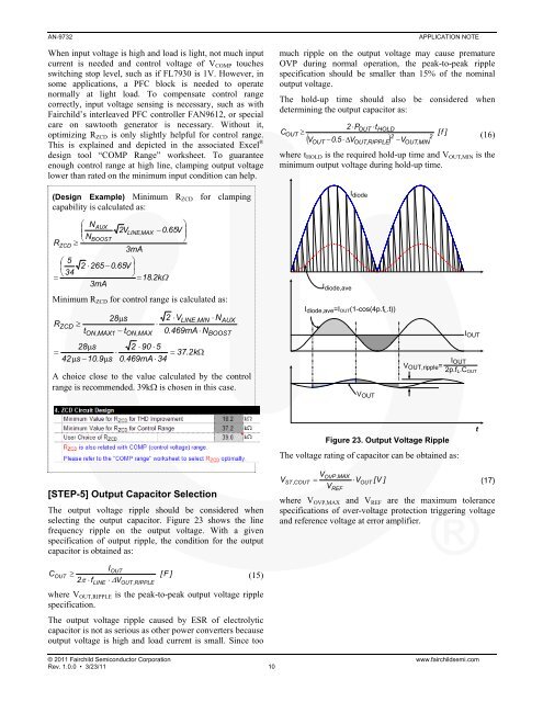
[STEP-5] Output Capacitor Selection<br />
The output voltage ripple should be considered when<br />
selecting the output capacitor. Figure 23 shows the line<br />
frequency ripple on the output voltage. With a given<br />
specification of output ripple, the condition for the output<br />
capacitor is obtained as:<br />
IOUT<br />
COUT<br />
[ F ]<br />
(15)<br />
2<br />
fLINE<br />
VOUT,<br />
RIPPLE<br />
where VOUT,RIPPLE is the peak-to-peak output voltage ripple<br />
specification.<br />
The output voltage ripple caused by ESR of electrolytic<br />
capacitor is not as serious as other power converters because<br />
output voltage is high and load current is small. Since too<br />
much ripple on the output voltage may cause premature<br />
OVP during normal operation, the peak-to-peak ripple<br />
specification should be smaller than 15% of the nominal<br />
output voltage.<br />
The hold-up time should also be considered when<br />
determining the output capacitor as:<br />
2<br />
POUT<br />
tHOLD<br />
COUT<br />
[ f ]<br />
2<br />
2<br />
(16)<br />
VOUT 0.<br />
5 V<br />
OUT,<br />
RIPPLE<br />
VOUT,<br />
MIN<br />
where tHOLD is the required hold-up time and VOUT,MIN is the<br />
minimum output voltage during hold-up time.<br />
Idiode,ave<br />
© 2011 <strong>Fairchild</strong> <strong>Semiconductor</strong> Corporation www.fairchildsemi.com<br />
Rev. 1.0.0 • 3/23/11 10<br />
Idiode<br />
Idiode,ave=IOUT(1-cos(4p.fL.t))<br />
VOUT<br />
IOUT<br />
VOUT,ripple= IOUT<br />
2p.fL.COUT<br />
Figure 23. Output Voltage Ripple<br />
The voltage rating of capacitor can be obtained as:<br />
VOVP,<br />
MAX<br />
V<br />
[ V ]<br />
(17)<br />
V<br />
VST , COUT<br />
OUT<br />
REF<br />
where VOVP,MAX and VREF are the maximum tolerance<br />
specifications of over-voltage protection triggering voltage<br />
and reference voltage at error amplifier.<br />
t


