

AN-3008 RC Snubber Networks for Thyristor Power Control and ...
AN-3008 RC Snubber Networks for Thyristor Power Control and ...
AN-3008 RC Snubber Networks for Thyristor Power Control and ...

Create successful ePaper yourself
Turn your PDF publications into a flip-book with our unique Google optimized e-Paper software.
<strong>AN</strong>-<strong>3008</strong><br />
APPLICATION NOTE<br />
TRIAC Design Procedure<br />
dV<br />
(<br />
dt<br />
) c<br />
dV<br />
1. Refer to Figure 18 <strong>and</strong> select a particular damping factor<br />
(ρ)giving a suitable trade-off between V PK <strong>and</strong> ------ .<br />
dt<br />
dV<br />
Determine the normalized ------ corresponding to the<br />
dt<br />
chosen damping factor.<br />
The volage E depends on the load phase angle:<br />
E 2 V RMS Sin (φ) where φ = tan – 1 X =<br />
⎛------<br />
L ⎞ where<br />
⎝R L<br />
⎠<br />
φ = measured phase angle between line V <strong>and</strong> load I<br />
R L = measured dc resistance of the load.<br />
dV<br />
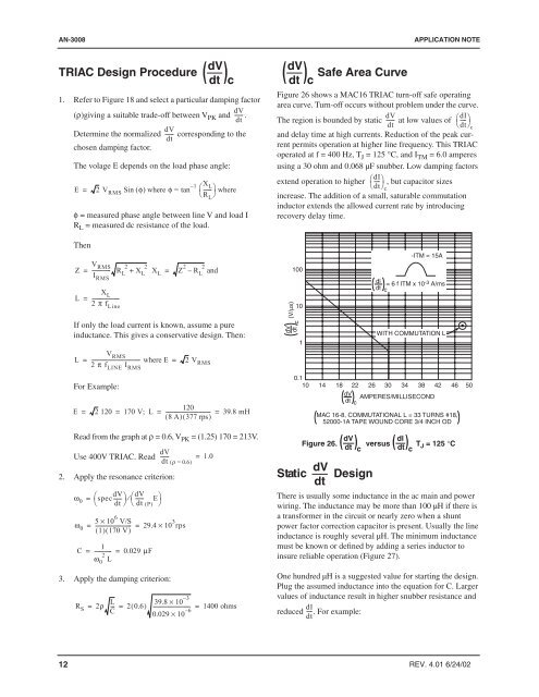
( Safe Area Curve<br />
dt<br />
) c<br />
dV<br />
Figure 26 shows a MAC16 TRIAC turn-off safe operating<br />
area curve. Turn-off occurs without problem under the curve.<br />
The region is bounded by static ------ at low values of ⎛dI<br />
----⎞<br />
dt<br />
⎝dt⎠c<br />
<strong>and</strong> delay time at high currents. Reduction of the peak current<br />
permits operation at higher line frequency. This TRIAC<br />
operated at f = 400 Hz, T J = 125 °C, <strong>and</strong> I TM = 6.0 amperes<br />
using a 30 ohm <strong>and</strong> 0.068 µF snubber. Low damping factors<br />
extend operation to higher ⎛dI<br />
----⎞<br />
⎝<br />
, but capacitor sizes<br />
dt⎠c<br />
increase. The addition of a small, saturable commutation<br />
inductor extends the allowed current rate by introducing<br />
recovery delay time.<br />
Then<br />
V RMS 2 2<br />
Z -------------- R<br />
I L + X L X L Z 2 2<br />
= = – R L <strong>and</strong><br />
RMS<br />
X<br />
L = --------------------- L<br />
2 π f Line<br />
If only the load current is known, assume a pure<br />
inductance. This gives a conservative design. Then:<br />
V RMS<br />
L = --------------------------------------- where E = 2 V<br />
2 π f LINE I RMS<br />
RMS<br />
For Example:<br />
120<br />
E = 2 120 = 170 V; L = ----------------------------------- = 39.8 mH<br />
( 8 A) ( 377 rps)<br />
(V/µs)<br />
100<br />
10<br />
c<br />
dV<br />
dt<br />
1<br />
0.1<br />
10<br />
dl<br />
dt<br />
-ITM = 15A<br />
c = 6 f ITM x 10-3 A/ms<br />
WITH COMMUTATION L<br />
14 18 22 26 30 34 38 42 46 50<br />
dV<br />
AMPERES/MILLISECOND<br />
dt c<br />
MAC 16-8, COMMUTATIONAL L = 33 TURNS #18,<br />
52000-1A TAPE WOUND CORE 3/4 INCH OD<br />
Read from the graph at ρ = 0.6, V PK = (1.25) 170 = 213V.<br />
dV<br />
Use 400V TRIAC. Read ------ = 1.0<br />
dt ( ρ = 0.6)<br />
2. Apply the resonance criterion:<br />
ω ⎛ 0 spec dV ------ ⎞ dV<br />
= ⁄ ⎛------ E⎞<br />
⎝ dt ⎠ ⎝ dt ( P)<br />
⎠<br />
510 × 6 V/S<br />
ω 0 = ---------------------------- =<br />
( 1) ( 170 V)<br />
29.4 × 10 3 rps<br />
1<br />
C = ------------- = 0.029 µF<br />
2<br />
ω 0 L<br />
3. Apply the damping criterion:<br />
R S 2ρ L 39.8 × 10 – 3<br />
= --- = 2( 0.6)<br />
C ------------------------------ 0.029 × 10 – 6 = 1400 ohms<br />
Static<br />
dl<br />
( ) c<br />
( ) c<br />
dV<br />
Figure 26.<br />
dt<br />
versus<br />
dt<br />
T J = 125 °C<br />
dV<br />
dt<br />
Design<br />
There is usually some inductance in the ac main <strong>and</strong> power<br />
wiring. The inductance may be more than 100 µH if there is<br />
a trans<strong>for</strong>mer in the circuit or nearly zero when a shunt<br />
power factor correction capacitor is present. Usually the line<br />
inductance is roughly several µH. The minimum inductance<br />
must be known or defined by adding a series inductor to<br />
insure reliable operation (Figure 27).<br />
One hundred µH is a suggested value <strong>for</strong> starting the design.<br />
Plug the assumed inductance into the equation <strong>for</strong> C. Larger<br />
values of inductance result in higher snubber resistance <strong>and</strong><br />
dI<br />
reduced ---- . For example:<br />
dt<br />
12 REV. 4.01 6/24/02


