

AN-3008 RC Snubber Networks for Thyristor Power Control and ...
AN-3008 RC Snubber Networks for Thyristor Power Control and ...
AN-3008 RC Snubber Networks for Thyristor Power Control and ...

Create successful ePaper yourself
Turn your PDF publications into a flip-book with our unique Google optimized e-Paper software.
APPLICATION NOTE<br />
<strong>AN</strong>-<strong>3008</strong><br />
27<br />
DIFFERENTIAL<br />
PREAMP<br />
X100 PROBE<br />
X100 PROBE<br />
G<br />
2<br />
1<br />
V DRM/V RRM SELECT<br />
DUT<br />
20k 2W<br />
2W<br />
0.33 1000V<br />
1000<br />
10 WATT<br />
WIREWOUND<br />
0.047<br />
1000V<br />
R GK<br />
470pF<br />
MOUNT DUT ON<br />
TEMPERATURE CONTROLLED<br />
Cµ PLATE<br />
dV<br />
dt<br />
VERNIER<br />
100<br />
2W<br />
82<br />
2W<br />
0.001<br />
0.005<br />
0.01<br />
0.047<br />
POWER<br />
1 MEG 2W EACH<br />
1.2 MEG<br />
2W<br />
TEST<br />
1N914<br />
0.1<br />
20V<br />
f = 10 Hz<br />
PW = 100 µs<br />
50 Ω PULSE<br />
GENERATOR<br />
56<br />
2W<br />
1000<br />
1/4W<br />
1N967A<br />
18V<br />
MTP1N100<br />
0.47<br />
0-1000V<br />
10mA<br />
ALL COMPONENTS ARE NON-INDUCTIVE UNLESS SHOWN<br />
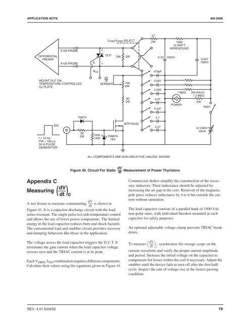
Figure 40. Circuit For Static<br />
dV<br />
dt<br />
Measurement of <strong>Power</strong> <strong>Thyristor</strong>s<br />
Appendix C<br />
Measuring<br />
dV<br />
(<br />
dt<br />
) c<br />
dV<br />
A test fixture to measure commutating ------ is shown in<br />
dt<br />
Figure 41. It is a capacitor discharge circuit with the load<br />
series resonant. The single pulse test aids temperature control<br />
<strong>and</strong> allows the use of lower power components. The limited<br />
energy in the load capacitor reduces burn <strong>and</strong> shock hazards.<br />
The conventional load <strong>and</strong> snubber circuit provides recovery<br />
<strong>and</strong> damping behaviors like those in the application.<br />
The voltage across the load capacitor triggers the D.U.T. It<br />
terminates the gate current when the load capacitor voltage<br />
crosses zero <strong>and</strong> the TRIAC current is at its peak.<br />
Each V DRM , I TM combination requires different components.<br />
Calculate their values using the equations given in Figure 41.<br />
Commercial chokes simplify the construction of the necessary<br />
inductors. Their inductance should be adjusted by<br />
increasing the air gap in the core. Removal of the magnetic<br />
pole piece reduces inductance by 4 to 6 but extends the current<br />
without saturation.<br />
The load capacitor consists of a parallel bank of 1500 Vdc<br />
non-polar units, with individual bleeders mounted at each<br />
capacitor <strong>for</strong> safety purposes.<br />
An optional adjustable voltage clamp prevents TRIAC breakdown.<br />
To measure ⎛dV<br />
------ ⎞<br />
⎝<br />
, synchronize the storage scope on the<br />
dt ⎠c<br />
current wave<strong>for</strong>m <strong>and</strong> verify the proper current amplitude<br />
<strong>and</strong> period. Increase the initial voltage on the capacitor to<br />
compensate <strong>for</strong> losses within the coil if necessary. Adjust the<br />
snubber until the device fails to turn off after the first halfcycle.<br />
Inspect the rate of voltage rise at the fastest passing<br />
condition.<br />
REV. 4.01 6/24/02 19


