

AN-3008 RC Snubber Networks for Thyristor Power Control and ...
AN-3008 RC Snubber Networks for Thyristor Power Control and ...
AN-3008 RC Snubber Networks for Thyristor Power Control and ...

You also want an ePaper? Increase the reach of your titles
YUMPU automatically turns print PDFs into web optimized ePapers that Google loves.
<strong>AN</strong>-<strong>3008</strong><br />
APPLICATION NOTE<br />
I S<br />
H S M L<br />
= ------------------ where:<br />
0.4 π N<br />
H S = MMF to saturate = 0.5 Oersted<br />
ML = mean magnetic path length = 4.99 cm.<br />
(.5) (4.99)<br />
I S = ----------------------- = 60 mA.<br />
0.4 π 33<br />
<strong>Snubber</strong> Physics<br />
Undamped Natural Resonance<br />
I<br />
ω 0 = -----------Radians/second<br />
LC<br />
dV<br />
Resonance determines ------ <strong>and</strong> boosts the peak capacitor<br />
dt<br />
voltage when the snubber resistor is small. C <strong>and</strong> L are<br />
related to one another by ω 2 dV<br />
0 . ------ scales linearly with ω<br />
dt<br />
0<br />
when the damping factor is held constant. A ten to one<br />
dV<br />
reduction in ------ requires a 100 to 1 increase in either<br />
dt<br />
component.<br />
Damping Factor<br />
ρ =<br />
The damping factor is proportional to the ratio of the circuit<br />
loss <strong>and</strong> its surge impedance. It determines the trade off<br />
dV<br />
between ------ <strong>and</strong> peak voltage. Damping factors between<br />
dt<br />
0.01 <strong>and</strong> 1.0 are recommended.<br />
The <strong>Snubber</strong> Resistor<br />
dV<br />
Damping <strong>and</strong><br />
dt<br />
dV<br />
When ρ < 0.5, the snubber resistor is small, <strong>and</strong> ------ depends<br />
dt<br />
dV<br />
mostly on resonance. There is little improvement in ------ <strong>for</strong><br />
dt<br />
damping factors less than 0.3, but peak voltage <strong>and</strong> snubber<br />
discharge current increase. The voltage wave has a 1-COS(θ)<br />
dV<br />
shape with overshoot <strong>and</strong> ringing. Maximum ------ occurs at a<br />
dt<br />
time later than t = 0. There is a time delay be<strong>for</strong>e the<br />
voltage rise, <strong>and</strong> the peak voltage almost doubles.<br />
When ρ > 0.5, the voltage wave is nearly exponential in<br />
dV<br />
shape. The maximum instantaneous ------ occurs at t = 0.<br />
dt<br />
There is little time delay <strong>and</strong> moderate voltage overshoot.<br />
R<br />
---<br />
2<br />
dV<br />
When ρ > 1.0, the snubber resistor is large <strong>and</strong> ------ depends<br />
dt<br />
mostly on its value. There is some overshoot even though the<br />
circuit is overdamped.<br />
C<br />
---<br />
L<br />
High load inductance requires large snubber resistors <strong>and</strong><br />
small snubber capacitors. Low inductances imply small<br />
resistors <strong>and</strong> large capacitors.<br />
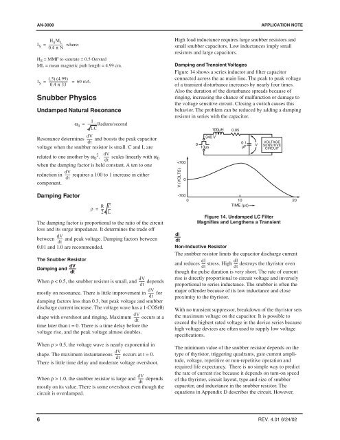
Damping <strong>and</strong> Transient Voltages<br />
Figure 14 shows a series inductor <strong>and</strong> filter capacitor<br />
connected across the ac main line. The peak to peak voltage<br />
of a transient disturbance increases by nearly four times.<br />
Also the duration of the disturbance spreads because of<br />
ringing, increasing the chance of malfunction or damage to<br />
the voltage sensitive circuit. Closing a switch causes this<br />
behavior. The problem can be reduced by adding a damping<br />
resistor in series with the capacitor.<br />
+700<br />
V (VOLTS)<br />
0<br />
-700<br />
0<br />
10µs<br />
340 V<br />
100µH 0.05<br />
0.1<br />
µF<br />
0 10 20<br />
TIME (µs)<br />
Figure 14. Undamped LC Filter<br />
Magnifies <strong>and</strong> Lengthens a Transient<br />
dl<br />
dt<br />
Non-Inductive Resistor<br />
The snubber resistor limits the capacitor discharge current<br />
dI<br />
dI<br />
<strong>and</strong> reduces ---- stress. High ---- destroys the thyristor even<br />
dt<br />
dt<br />
though the pulse duration is very short. The rate of current<br />
rise is directly proportional to circuit voltage <strong>and</strong> inversely<br />
proportional to series inductance. The snubber is often the<br />
major offender because of its low inductance <strong>and</strong> close<br />
proximity to the thyristor.<br />
With no transient suppressor, breakdown of the thyristor sets<br />
the maximum voltage on the capacitor. It is possible to<br />
exceed the highest rated voltage in the device series because<br />
high voltage devices are often used to supply low voltage<br />
specifications.<br />
The minimum value of the snubber resistor depends on the<br />
type of thyristor, triggering quadrants, gate current amplitude,<br />
voltage, repetitive or non-repetitive operation <strong>and</strong><br />
required life expectancy. There is no simple way to predict<br />
the rate of current rise because it depends on turn-on speed<br />
of the thyristor, circuit layout, type <strong>and</strong> size of snubber<br />
capacitor, <strong>and</strong> inductance in the snubber resistor. The<br />
equations in Appendix D describes the circuit. However,<br />
V<br />
VOLTAGE<br />
SENSITIVE<br />
CI<strong>RC</strong>UIT<br />
6 REV. 4.01 6/24/02


