Chapter 1 Review of Basic Semiconductor Physics - courses.cit ...
Chapter 1 Review of Basic Semiconductor Physics - courses.cit ...
Chapter 1 Review of Basic Semiconductor Physics - courses.cit ...

Create successful ePaper yourself
Turn your PDF publications into a flip-book with our unique Google optimized e-Paper software.
<strong>Semiconductor</strong> Optoelectronics (Farhan Rana, Cornell University)<br />
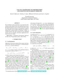
The bandstructures <strong>of</strong> Si, Ge , and GaAs are shown below.<br />
Germanium bandstructure Silicon bandstructure GaAs bandstructure<br />
Only few chosen bands are shown. A particular feature <strong>of</strong> all semiconductor is that electrons in<br />
semiconductors fill all the low lying energy bands (called the valence bands). There are four valence<br />
bands, but only the highest three are shown in the figure. The highest energy in the valence bands is<br />
denoted by E v . In pure semiconductors the conduction bands are all empty on electrons. The lowest<br />
energy in the conduction bands is denoted by E c . There are also four conduction bands and all four are<br />
shown in the figure. The difference Ec Ev<br />
Eg<br />
is called the band gap <strong>of</strong> the semiconductor.<br />
Near the bottom <strong>of</strong> the<br />
<br />
lowest conduction band and the top <strong>of</strong> the highest valence band one may Taylor<br />
expand the energy En k .<br />
Assuming isotropic parabolic bands, conduction band dispersion near the band<br />
bottom can be written as,<br />
2<br />
<br />
k E k K c k K c <br />
Ec c<br />
<br />
2me<br />
And for the valence band one can write,<br />
2<br />
<br />
k E k K v k K v <br />
Ev v<br />
<br />
2mh<br />
where m e and m h are electron and hole effective masses and the vectors K c and K v are the locations<br />
in k-space <strong>of</strong> conduction band minimum and valence band maximum. K v 0 for all semiconductors that<br />
we will consider. K c 0 for most III-V and II-VI semiconductors. <strong>Semiconductor</strong>s for which Kc Kv<br />
are called “direct gap” or just “direct (e.g. GaAs, InP , GaN , ZnSe, CdSe, ZnO). <strong>Semiconductor</strong>s<br />
for which K c K v are called “indirect gap” or just “indirect” (e.g. Si, Ge , C , SiC , GaP , AlAs ).<br />
As we will see later in the course, all optically active semiconductors are direct gap.<br />
When K c Kv<br />
0 , and assuming isotropic parabolic bands,<br />
Conduction band: E k <br />
c<br />
2 2<br />
k<br />
Ec<br />
<br />
2me