Improved Circuit Model of Photovoltaic Array - courses.cit.cornell.edu
Improved Circuit Model of Photovoltaic Array - courses.cit.cornell.edu
Improved Circuit Model of Photovoltaic Array - courses.cit.cornell.edu

You also want an ePaper? Increase the reach of your titles
YUMPU automatically turns print PDFs into web optimized ePapers that Google loves.
International Journal <strong>of</strong> Electrical Power and Energy Systems Engineering 2:3 2009<br />
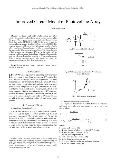
<strong>Improved</strong> <strong>Circuit</strong> <strong>Model</strong> <strong>of</strong> <strong>Photovoltaic</strong> <strong>Array</strong><br />
Abstract—A circuit based model <strong>of</strong> photovoltaic array (PV)<br />
suitable for simulation studies <strong>of</strong> solar power systems is proposed in<br />
this paper. The proposed model is realised using Power System<br />
Block Set under MATLAB/SIMULINK, however, it can be<br />
constructed using standard simulation s<strong>of</strong>tware such as PSPICE. The<br />
proposed circuit model has several advantages: simple, reliable,<br />
allows simulation <strong>of</strong> basic cells, group <strong>of</strong> cells, or mismatched panels<br />
that work under different operating conditions. The obtained results<br />
<strong>of</strong> both uniform and mismatched PVs prove the validity <strong>of</strong> the<br />
proposed model to simulate the non-linear behaviour <strong>of</strong> photovoltaic<br />
array not only to understand the operation <strong>of</strong> PV systems but also to<br />
design a proper maximum power point tracker to extract the<br />
maximum possible power from the photovoltaic array.<br />
Keywords—<strong>Photovoltaic</strong> array, piecewise linear model,<br />
modelling, simulation.<br />
I. INTRODUCTION<br />
ENEWABLE energy sources are gaining more interest in<br />
R recent years. Among them, photovoltaic (PV) panels, that<br />
<strong>of</strong>fer several advantages such as requirement <strong>of</strong> little<br />
maintenance, no environmental pollution. Recently, PV arrays<br />
are used in many applications such as battery chargers, solar<br />
powered water pumping systems, grid connected PV systems,<br />
solar hybrid vehicles, and satellite power systems. In all solar<br />
power systems, efficient simulations including PV panel are<br />
required before any experimental verification. The aim <strong>of</strong> this<br />
paper is to present a circuit-based model <strong>of</strong> PV array that can<br />
be utilized in any simulation studies <strong>of</strong> such solar power<br />
systems.<br />
II. CLASSICAL PV MODEL<br />
A. Simplified Equivalent <strong>Circuit</strong><br />
A solar cell basically is a p-n semiconductor junction.<br />
When exposed to light, a current proportional to solar<br />
irradiance isgenerated. The circuit model <strong>of</strong> PV cell is<br />
iluustrated in Fig. 1. Standard simulation tools utilize the<br />
approximate diode equivalent circuit shown in Fig. 2 in order<br />
to simulate all electric circuits that contain diodes. The model<br />
is based on two-segment piecewise linear approximation. The<br />
circuit consists <strong>of</strong> Ron in series with voltage source Von.<br />
Mohamed Azab is a lecturer in the Department <strong>of</strong> Electrical Engineering<br />
Technology at Banha High Institute <strong>of</strong> Technology, Banha, University. He<br />
holds Ph.D. degree (2002) from Politechnic University <strong>of</strong> Catalonia (UPC) –<br />
Spain. His research interests include power electronics and renewable energy<br />
sources (phones: 002013-3-230-297; 002013-3-25 42 38, e-mail: pe_bhit@<br />
yahoo.com, mohazab@lycos.com).<br />
Mohamed Azab<br />
185<br />
Fig. 2 Diode equivalent circuit used in Power System<br />
blockset/Simulink<br />
Fig. 3 Two-segment Diode model<br />
B. Theoretical Mathematical <strong>Model</strong><br />
The equations that describe I-V characteristics <strong>of</strong> the solar<br />
cell based on simple equivalent circuit shown in Fig. 1, are<br />
given below;<br />
I<br />
D<br />
I =<br />
=<br />
I<br />
L<br />
IL<br />
I<br />
o<br />
−<br />
(e<br />
I<br />
o<br />
q(V + IR s )<br />
kT<br />
(e<br />
ID<br />
Fig. 1 <strong>Circuit</strong> model <strong>of</strong> PV solar cell<br />
i D<br />
+<br />
VD<br />
1<br />
Ish<br />
iD<br />
q(V + IR s )<br />
kT<br />
− 1)<br />
V + IR<br />
− 1) -<br />
R<br />
Where:<br />
I is the cell current (A).<br />
q is the charge <strong>of</strong> electron = 1.6x10 -19 (coul).<br />
K is the Boltzman constant (j/K).<br />
T is the cell temperature (K).<br />
IL is the light generated current (A).<br />
Io is the diode saturation current.<br />
Rs , Rsh are cell series and shunt resistance (ohms).<br />
V is the cell output voltage (V).<br />
Rsh<br />
Rs<br />
Ron<br />
Vo<br />
n<br />
I<br />
Ideal diode<br />
2<br />
sh<br />
s<br />
+<br />
V<br />
-<br />
V D<br />
(1)<br />
(2)
III. PROPOSED PV CIRCUIT MODEL<br />
A. Proposed Piecewise Linear <strong>Model</strong><br />
In this paper bP 350U Solar Panel is chosen to verify the<br />
proposed circuit model. The panel has 36 series connected<br />
cells. The key specifications <strong>of</strong> the bP 350U PV Solar Panel<br />
are shown in Table I.<br />
TABLE I<br />
KEY SPECIFICATION OF BP SOLAR PANEL<br />
Maximum Power Pmax 50 W<br />
Voltage @ max. power Vmax 17.3 V<br />
Current @ max. power Imax 2.89 A<br />
Short circuit current ISC 3.17 A<br />
Open circuit voltage VOC 21.8 V<br />
The piecewise linear model developed in this paper is based<br />
substituting single-diode by three-parallel diodes. Each diode<br />
is modelled as simple piecewise linear (PWL) as a voltage<br />
controlled resistor with two states ON and OFF as shown in<br />
Fig. 4. Therefore, the V-I curve <strong>of</strong> the equivalent diode <strong>of</strong> the<br />
PV cell is approximated and divided into several segments.<br />
Each diode provides two-segments <strong>of</strong> the curve. In addition,<br />
the PWL model <strong>of</strong> the PV cell can be improved by<br />
approximating the curve with more segments by connecting<br />
more diodes in parallel with suitable values <strong>of</strong> series<br />
resistances. Computation <strong>of</strong> these series resistors will be<br />
explained in the following section. Fig. 5 shows the proposed<br />
PWL model <strong>of</strong> the PV cell.<br />
+<br />
VD<br />
D1<br />
Ron1<br />
Von1<br />
International Journal <strong>of</strong> Electrical Power and Energy Systems Engineering 2:3 2009<br />
Basically, the model is developed to simulate single PV<br />
cell. However, it is easy to scale up the model to account for<br />
the overall PV panel which consists <strong>of</strong> 36 cells connected in<br />
series. Scaling up to simulate the bulk PV panel is carried out<br />
using two methods:<br />
Ron2<br />
Von2<br />
Fig. 4 Proposed PWL <strong>Model</strong> <strong>of</strong> PV diode<br />
1. Bulk PV <strong>Model</strong>: Where the experimental data <strong>of</strong> bp solar<br />
panel are used to compute directly the values <strong>of</strong> diodes<br />
ON-voltages (VD1,VD2, and VD3) and series resistors (Ron1,<br />
Ron2, and Ron3) to account for the all 36 cells that are<br />
connected in series as given in manufacturer data sheet.<br />
2. Single PV cell <strong>Model</strong>: the basic PV solar cell, is modelled,<br />
then the total voltage produced from the panel is computed<br />
from: Vpanel = nVcell , while the current through all cells is<br />
identical. In circuit based-models, the overall PV panel<br />
model is also obtained by hardware connection <strong>of</strong><br />
individual cell to account for the all 36 solar cells.<br />
D3 D2<br />
Ron3<br />
Von3<br />
186<br />
B. Calculation <strong>of</strong> <strong>Model</strong> Parameters<br />
(1) Bulk PV <strong>Model</strong><br />
The proposed model approximates the I-V curve by four<br />
line segments as shown in Fig. (5b) taking into consideration<br />
the following:<br />
- PV parameters at maximum power point (MPP): Vmax =<br />
17.3 V, and Imax = 2.89 A.<br />
- Vertex points are located at:<br />
0.9 MPP , MPP , 1.1 MPP.<br />
- The model assumes that: Von1 < Von2 < Von3 .<br />
The operation in each segment is explained below:<br />
Segment 1: ( VD < Von1 )<br />
(Von1 = 0.9 MPP = 15.57 V). When the generated voltage is<br />
less than Von1 , all diodes are OFF, and no current flows<br />
through the diodes, thus the light generated current from PV<br />
flows through the load and a small portion can flow through<br />
the shunt resistance Rsh , therefore the current is nearly<br />
constant in this segment.<br />
Segment 2: ( Von1 < VD < Von2 )<br />
Diode D1 is ON.<br />
Since the PV current fails from 3.17 A to 2.89 A, thus the<br />
current through (diode D1) is 0.28 A.<br />
Ron1 is computed from the following equation:<br />
R<br />
on1<br />
I L<br />
Vmax<br />
− 0.9V max 17.<br />
3 − 15.<br />
57<br />
= =<br />
(3)<br />
I - 0<br />
0.<br />
28<br />
Ron1 = 6.17 Ω.<br />
D1<br />
D1<br />
Ron1<br />
Von1<br />
Ron2<br />
Segment 3: ( Von2 < VD < Von3 )<br />
Diodes D1 and D2 are ON.<br />
The current through D1 is calculated as follows:<br />
D2<br />
Von2<br />
D3<br />
Ron3<br />
Von3<br />
RP<br />
RS<br />
Fig. 5a Proposed PWL <strong>Model</strong> <strong>of</strong> PV cell<br />
iD<br />
VD<br />
Fig. 5b Proposed diode model<br />
I<br />
+<br />
V<br />
-
I<br />
D1<br />
1.1V max − 0.9V max 3.<br />
46<br />
= = = 0.<br />
56 A<br />
(4)<br />
R<br />
6.<br />
17<br />
on1<br />
Since the PV output current is 2 A, the current through diode<br />
D2:<br />
ID2 = ILG –ID1 – Io = 3.17 - 0.56 - 2 (5)<br />
ID2 = 0.61 A.<br />
Ron2 is computed from the following equation:<br />
R<br />
on2<br />
1.1V max − Vmax<br />
19.<br />
03 − 17.<br />
3<br />
= =<br />
(6)<br />
I - 0<br />
0.<br />
61<br />
Ron2 = 2.83 Ω.<br />
D2<br />
Segment 4: ( Von3 < VD < VOC )<br />
All Diodes are ON.<br />
The PV load current is zero at open circuit point, the open<br />
circuit voltage is 21.8 V.<br />
The current through D1 is calculated from eqn. (10):<br />
I<br />
D1<br />
VOC<br />
− 1.1V max 2.<br />
77<br />
= = = 0.<br />
44 A<br />
(7)<br />
R<br />
6.<br />
17<br />
on1<br />
The current through diode D2 is computed:<br />
I<br />
D2<br />
VOC<br />
− 1.1V max 2.<br />
77<br />
= = = 0.<br />
97 A<br />
(8)<br />
R<br />
2.<br />
83<br />
on2<br />
Since the PV output current is zero, the current through diode<br />
D3 is computed from:<br />
ID3 = ILG – ID1 – ID2 – Io (9)<br />
ID3 = 3.17 - 0.44 – 0.97 - 0 = 1.76 A.<br />
Ron3 is computed from equation (13) :<br />
International Journal <strong>of</strong> Electrical Power and Energy Systems Engineering 2:3 2009<br />
R on3<br />
VOC<br />
− 1.<br />
1Vmax<br />
=<br />
I D3 - 0<br />
21.<br />
8 − 19.<br />
03<br />
=<br />
(10)<br />
1.<br />
76<br />
Ron3 = 1.57 Ω.<br />
(2) Single PV Cell<br />
The same method is used to compute the cell parameters.<br />
But, in this case the cell voltage at maximum point is 17.3/36<br />
= 0.48 V. Consequently, Von1, Von2 and Von3 are scaled to be<br />
0.432 V, 0.48 V, and 0.528 V respectively. The current values<br />
are the same because all cells are connected in series. So the<br />
same current flows in all cells.<br />
It is important to mention that, vertex points can take other<br />
values instead <strong>of</strong> (0.9MPP, MPP, 1.1MPP) as presented in<br />
reference [4]. One <strong>of</strong> the major advantages <strong>of</strong> the proposed<br />
model, that it is easy to readjust the vertex points and the<br />
187<br />
corresponding model calculations in order to match (fit) the<br />
experimental results <strong>of</strong> a certain PV panel.<br />
IV. SIMULATION RESULTS<br />
A. Proposed PV <strong>Model</strong><br />
The proposed PV model is verified using power System<br />
block set under Matlab/Simulink. Within the model, vertex<br />
points <strong>of</strong> (I-V) curve can be adjusted according to previously<br />
presented eqns. (6) to (12). V-I curve, and V-P curve <strong>of</strong> the<br />
overall PV bulk model are illustrated in Fig. 6 and Fig. 7<br />
respectively.<br />
I (A)<br />
Fig. 6 I-V curve with the proposed model<br />
Fig. 7 P-V curve with the proposed model<br />
Fig. 6 presents the I-V curve obtained from the proposed<br />
model. The segments <strong>of</strong> the I-V curve can be observed easily.<br />
Fig. 7 illustrates the corresponding P-V curve. The light<br />
generated current is 3.2 A. Fig. 8 and Fig. 9 demonstrate the<br />
behaviour <strong>of</strong> the PV under different levels <strong>of</strong> irradiations.<br />
Inside the model, irradiation level can be changed by setting<br />
the value <strong>of</strong> light generated current to the required value. They<br />
are selected to be 3.1 A, 2.6 A, and 2 A. The I-V family<br />
curves are plotted in Fig. 8, while the P-V family curves are<br />
plotted in Fig. 9.<br />
I (A)<br />
3<br />
2<br />
1<br />
P (W)<br />
0<br />
0 5 10 15 20 25<br />
60<br />
40<br />
20<br />
3<br />
2<br />
1<br />
1<br />
V (v)<br />
V (v)<br />
0<br />
0 5 10 15 20 25<br />
2<br />
V (v)<br />
0<br />
0 5 10 15 20 25<br />
Fig. 8 I-V family curves with proposed model for different irradiation<br />
levels<br />
3
P (W)<br />
60<br />
40<br />
20<br />
1) I = 3.1 A 2) I = 2.6 A 3) I = 2 A<br />
0<br />
0 5 10 15 20 25<br />
V (v)<br />
Fig. 9 P-V family curves with proposed model for different<br />
irradiation levels<br />
B. Classical PV <strong>Model</strong><br />
In addition to the proposed PV model, classical PV model<br />
is also carried out for comparison. Simulation results <strong>of</strong> PV<br />
using classical circuit model are presented in Fig. 10 and Fig.<br />
11.<br />
4<br />
I (A)<br />
3<br />
2<br />
1<br />
International Journal <strong>of</strong> Electrical Power and Energy Systems Engineering 2:3 2009<br />
0<br />
0 5 10 15 20 25<br />
V (v)<br />
Fig. 10 I-V curve with classical model<br />
60<br />
50<br />
40<br />
P (W) 30<br />
20<br />
10<br />
0<br />
0 5 10 15 20 25<br />
V (v)<br />
Fig. 11 P-V curve with classical model<br />
According to the obtained results, the proposed model <strong>of</strong>fer<br />
better waveforms for I-V and P-V curves. While classical PV<br />
model produces abrupt change in the slope <strong>of</strong> P-V curve and<br />
I-V curve observed in Fig. 10 and Fig. 11.<br />
C. Mismatched PV Panels<br />
The proposed PV model is also used to simulate<br />
mismatched PV panels when exposed to different solar<br />
irradiance. In this section two mismatched PV panels<br />
connected in series are simulated. The irradiation levels are<br />
adjusted such that the light generated currents are 3 A and 1<br />
A.<br />
2<br />
1<br />
3<br />
188<br />
The corresponding P-V curve is shown in Fig. 12. It is clear<br />
that the curve exhibits two maxima at two different voltage<br />
levels which is similar to what happens in real operation.<br />
P (W)<br />
60<br />
50<br />
40<br />
30<br />
20<br />
10<br />
0<br />
0 5 10 15 20 25 30 35 40<br />
V (v)<br />
Fig. 12 P-V curve <strong>of</strong> simulated mismatched PV Panels<br />
V. CONCLUSION<br />
This paper presents simplified piecewise linear model for<br />
PV solar panels suitable for power electronics simulation<br />
studies. The proposed circuit model accounts also for the<br />
behaviour <strong>of</strong> mismatched PV panels. The obtained results<br />
prove the validity <strong>of</strong> the proposed model to simulate the PV<br />
with considerable accuracy under different operating<br />
conditions.<br />
REFERENCES<br />
[1] E. V. Solodovnik, S. Liu, and R. A. Dougal, "Power Controller Design<br />
for Maximum Power Tracking in Solar Installations," IEEE Trans.<br />
Power Electron., vol. 19, pp. 1295-1304, Sept. 2004.<br />
[2] Y.T. Tan; et. al.; “A <strong>Model</strong> <strong>of</strong> PV Generation Suitable for stability<br />
analysis ”, IEEE Trans. On energy Conv., Vol. 19, No. 4, 2004.<br />
[3] J. A. Jiang; et. al , “Maximum power tracking for photovoltaic power<br />
systems”, Tamkang Journal <strong>of</strong> Science and Engineering, Vol. 8, No. 2,<br />
pp. 147-153, 2005.<br />
[4] Ryan Campbell , “A circuit-based photovoltaic array model for power<br />
system studies”, Proceedings <strong>of</strong> the 39th North American Power<br />
Symposium (NAPS 2007), Las Cruces, NM, USA, October 2007.<br />
[5] E. Koutroulis; et. al, “Development <strong>of</strong> a Microcontroller-based<br />
photovoltaic maximum power tracking control system”, IEEE Trans. On<br />
power Electronics, Vol. 16, No. 1, pp. 46-54, 2001.<br />
[6] T.Y. Kim, et. al., "A novel maximum power point tracking control for<br />
photovoltaic power system under rapidly changing solar radiation," in<br />
IEEE International Symp. on Ind. Electron., pp. 1011-1014, 2001.