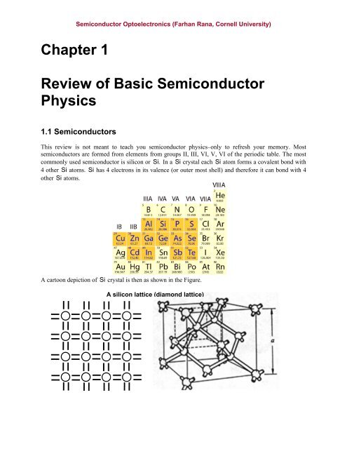
Chapter 1 Review of Basic Semiconductor Physics - courses.cit ...
Chapter 1 Review of Basic Semiconductor Physics - courses.cit ...
Chapter 1 Review of Basic Semiconductor Physics - courses.cit ...

Create successful ePaper yourself
Turn your PDF publications into a flip-book with our unique Google optimized e-Paper software.
<strong>Semiconductor</strong> Optoelectronics (Farhan Rana, Cornell University)<br />
<strong>Chapter</strong> 1<br />
<strong>Review</strong> <strong>of</strong> <strong>Basic</strong> <strong>Semiconductor</strong><br />
<strong>Physics</strong><br />
1.1 <strong>Semiconductor</strong>s<br />
This review is not meant to teach you semiconductor physics–only to refresh your memory. Most<br />
semiconductors are formed from elements from groups II, III, VI, V, VI <strong>of</strong> the periodic table. The most<br />
commonly used semiconductor is silicon or Si. In a Si crystal each Si atom forms a covalent bond with<br />
4 other Si atoms. Si has 4 electrons in its valence (or outer most shell) and therefore it can bond with 4<br />
other Si atoms.<br />
A cartoon depiction <strong>of</strong> Si crystal is then as shown in the Figure.<br />
A silicon lattice (diamond lattice)
<strong>Semiconductor</strong> Optoelectronics (Farhan Rana, Cornell University)<br />
In a Si crystal each Si atom bonds with 4 other Si atoms in a tetrahedral geometry, as shown. This<br />
structure is called a “diamond Lattice” (since diamond crystals consisting <strong>of</strong> C atoms also have the same<br />
structure). The diamond lattice is essentially an FCC lattice (face centered cubic) with a single-atom<br />
basis. The lattice constant ‘a’ is also shown in the figure. Note that ‘a’ is not the actual distance between<br />
the nearest Si atoms. ‘a’ is the length <strong>of</strong> one side <strong>of</strong> the diamond unit cell (not the wigner-seitz cell) that<br />
has the cubic symmetry. <strong>Semiconductor</strong>s are also formed by combining elements from group III and<br />
group V <strong>of</strong> the periodic table. This is possible since group III elements have 3 electrons in their outer<br />
most shell and group V elements have 5 electrons in their outermost shell. So a III-V covalent bond is<br />
possible. Most common III-V semiconductors are GaAs and In P .<br />
A GaAs lattice (zincblende lattice)<br />
Each Ga atom is surrounded by 4 As atoms and each As atom is surrounded by 4 Ga atoms in a<br />
tetrahederal geometry. GaAs lattice is an example <strong>of</strong> “zinc blende lattice”. The difference between zinc<br />
blende and diamond lattices is that in diamond lattice all atoms are the same. InP also has a zinc blende<br />
lattice. GaAs and InP are examples <strong>of</strong> “compound semiconductors”. Si, C, and Ge are examples <strong>of</strong><br />
“elemental semiconductors”. Not all compound semiconductors have the zinc blende lattice. For example,<br />
III-Nitrides (e.g GaN , AIN,InN ) can also have the wurtzite lattice structure show below.<br />
A GaN lattice (wurtzite lattice)
<strong>Semiconductor</strong> Optoelectronics (Farhan Rana, Cornell University)<br />
Just like the zinc blende lattice is a FCC lattice with a single-atom basis, the wurtzite lattice is a HCP<br />
c<br />
lattice (hexagonal close packed) with a single-atom basis. For ideal HCP lattice <br />
a<br />
thing common in zinc blende and wurtzite lattices; both have tetrahederal coordination.<br />
8<br />
3<br />
. There is one<br />
Group II elements and group VI elements also combine to give II-VI compound semiconductor like<br />
ZnSe, CdTe, CdSe, ZnO etc. Most <strong>of</strong> these have zine blende or wurtzite lattices (but some do have<br />
“rock salt” lattic structures). Most <strong>of</strong> the IV–VI semiconductors (e.g PbS, PbSe, PbTe ) called “lead<br />
salts” have the “rock salt” structure (similar to a NaCl crystal).<br />
1.2 <strong>Semiconductor</strong> Bandstructure<br />
In a solid the electronic energy levels are obtained by solving the Schrodinger Equation<br />
2<br />
<br />
2 <br />
V r rE r (1)<br />
<br />
2m<br />
<br />
where V r is the periodic potential from the atoms sitting on the lattice sites. The solutions <strong>of</strong> (1) can be<br />
written as,<br />
ik<br />
r<br />
r r e u r <br />
n , k<br />
n,<br />
k<br />
The eigenfunctions r n k<br />
<br />
,<br />
2<br />
<br />
2<br />
V r r E k r <br />
are called Bloch functions and satisfy,<br />
n , k n n,<br />
k<br />
<br />
2m<br />
<br />
The vector k can take values belonging to the first Brillouin zone (FBZ) and 'n ' takes integral values.<br />
Therefore, all the possible energy levels <strong>of</strong> the solid can be labeled by the set <strong>of</strong> values n, k.<br />
If one plots<br />
k <br />
En as a function <strong>of</strong> k for different integral values <strong>of</strong> n one obtains the bandstructure <strong>of</strong> the solid. The<br />
first Brillouin zone (FBZ) corresponding to a FCC lattice (or a diamond or a zinc blende lattice) is<br />
shown below.<br />
FBZ <strong>of</strong> an FCC lattice
<strong>Semiconductor</strong> Optoelectronics (Farhan Rana, Cornell University)<br />
The bandstructures <strong>of</strong> Si, Ge , and GaAs are shown below.<br />
Germanium bandstructure Silicon bandstructure GaAs bandstructure<br />
Only few chosen bands are shown. A particular feature <strong>of</strong> all semiconductor is that electrons in<br />
semiconductors fill all the low lying energy bands (called the valence bands). There are four valence<br />
bands, but only the highest three are shown in the figure. The highest energy in the valence bands is<br />
denoted by E v . In pure semiconductors the conduction bands are all empty on electrons. The lowest<br />
energy in the conduction bands is denoted by E c . There are also four conduction bands and all four are<br />
shown in the figure. The difference Ec Ev<br />
Eg<br />
is called the band gap <strong>of</strong> the semiconductor.<br />
Near the bottom <strong>of</strong> the<br />
<br />
lowest conduction band and the top <strong>of</strong> the highest valence band one may Taylor<br />
expand the energy En k .<br />
Assuming isotropic parabolic bands, conduction band dispersion near the band<br />
bottom can be written as,<br />
2<br />
<br />
k E k K c k K c <br />
Ec c<br />
<br />
2me<br />
And for the valence band one can write,<br />
2<br />
<br />
k E k K v k K v <br />
Ev v<br />
<br />
2mh<br />
where m e and m h are electron and hole effective masses and the vectors K c and K v are the locations<br />
in k-space <strong>of</strong> conduction band minimum and valence band maximum. K v 0 for all semiconductors that<br />
we will consider. K c 0 for most III-V and II-VI semiconductors. <strong>Semiconductor</strong>s for which Kc Kv<br />
are called “direct gap” or just “direct (e.g. GaAs, InP , GaN , ZnSe, CdSe, ZnO). <strong>Semiconductor</strong>s<br />
for which K c K v are called “indirect gap” or just “indirect” (e.g. Si, Ge , C , SiC , GaP , AlAs ).<br />
As we will see later in the course, all optically active semiconductors are direct gap.<br />
When K c Kv<br />
0 , and assuming isotropic parabolic bands,<br />
Conduction band: E k <br />
c<br />
2 2<br />
k<br />
Ec<br />
<br />
2me
Valence band: E k <br />
<strong>Semiconductor</strong> Optoelectronics (Farhan Rana, Cornell University)<br />
v<br />
2 2<br />
k<br />
Ev<br />
<br />
2mh<br />
More generally, one can write for the conductions band with minimum at K c (assuming parabolic<br />
bands),<br />
2<br />
<br />
1<br />
Ec k Ec<br />
k K c Me<br />
k K c <br />
2<br />
where M e is the effective mass matrix,<br />
mxx<br />
mxy<br />
mxz<br />
<br />
<br />
<br />
M e myx<br />
myy<br />
myz<br />
<br />
<br />
<br />
<br />
mzx<br />
mzy<br />
mzz<br />
<br />
Physical considerations demand that M e be symmetric. Similarly, for the valence band one get,<br />
2<br />
<br />
1<br />
k E k K v M k K v <br />
Ev v<br />
h<br />
<br />
2<br />
1.3 Counting Electronic States in <strong>Semiconductor</strong>s<br />
In a solid <strong>of</strong> volume V , the number <strong>of</strong> energy levels is one band in volume k <strong>of</strong> the FBZ is<br />
2 V<br />
3<br />
d k<br />
(The multiplies 2 accounts for the two spin states). So all summations <strong>of</strong> the from <br />
3 2<br />
where values <strong>of</strong> k are restricted to the FBZ can be replaced by the integral,<br />
3<br />
d k<br />
<br />
V<br />
<br />
3<br />
k FBZ 2 The number <strong>of</strong> energy levels per band in a crystal <strong>of</strong> volume V is given by,<br />
But,<br />
2<br />
<br />
2V<br />
<br />
2V<br />
3 2 2 3<br />
kFBZ FBZ <br />
<br />
d<br />
3<br />
k<br />
<br />
<br />
volume <strong>of</strong> FBZ<br />
2 <br />
volume <strong>of</strong> FBZ <br />
volume <strong>of</strong> the primitiveunit<br />
cell<br />
The number <strong>of</strong> energy levels per band in a crystal <strong>of</strong> volume V is then given by,<br />
V<br />
2 2 number <strong>of</strong> primitive cells in the crystal<br />
volume <strong>of</strong> the primitive cell<br />
3<br />
d 3<br />
<br />
Therefore each primitive cell contributes two states or energy levels to each band.<br />
kFBZ<br />
1.4 Linear Combination <strong>of</strong> Atomic Orbitals Approach to Energy Bands
<strong>Semiconductor</strong> Optoelectronics (Farhan Rana, Cornell University)<br />
Linear combination <strong>of</strong> atomic orbitals is another way to understand energy band formation in<br />
semiconductors. In semiconductors, the atomic states <strong>of</strong> the outermost shell (e.g the single 3s and the<br />
three 3p in a Si atom, and the single 4s and the three 4p in a Ga atom and the same in a As atom)<br />
combine or hybridize with the states <strong>of</strong> the neighboring atoms to result in the four valence bands and the<br />
four conditions bands, as shown in the figure below.<br />
In this hybridization process the total number <strong>of</strong> energy levels <strong>of</strong> all the atoms is conserved. Suppose N<br />
Si atoms from a crystal then the total number <strong>of</strong> energy levels before hybridization is 2 4N<br />
. Now lets<br />
find the total number <strong>of</strong> energy levels in the resulting crystal. As found earlier, the number <strong>of</strong> energy<br />
levels per band in a crystal <strong>of</strong> volume V is then given by,<br />
V<br />
2 2 number <strong>of</strong> primitive cells in the crystal<br />
volume <strong>of</strong> the primitive cell<br />
So the total number <strong>of</strong> energy levels in eight bands (four conduction bands and four valence bands) is,<br />
#<br />
<strong>of</strong> primitivecells<br />
#<br />
<strong>of</strong> <br />
2 <br />
<br />
in<br />
the crystal bands<br />
Since each Si primitive cell has two Si atoms (diamond lattice is an FCC lattice with a two-atom basis)<br />
we get,<br />
#<br />
<strong>of</strong> primitivecells<br />
#<br />
<strong>of</strong> N<br />
2 <br />
2 8 4N<br />
in<br />
the crystal bands<br />
2<br />
And we get the same answer as before.<br />
1.5 Properties <strong>of</strong> <strong>Semiconductor</strong> Alloys<br />
Other than elemental and compound semiconductors, semiconductor alloys also exist and are extremely<br />
useful. For example Si1 -x<br />
Gex<br />
is a binary allows <strong>of</strong> Si and Ge and the lattice <strong>of</strong> Si1 -x<br />
Gex<br />
consists <strong>of</strong><br />
x fraction <strong>of</strong> Ge atoms and 1 - x<br />
fraction <strong>of</strong> Si atoms arranged randomly. On the other hand SiC is a<br />
compound semiconductor with zinc blende Lattice.<br />
Binary Alloys:<br />
Si - Ge<br />
fraction <strong>of</strong> Si atoms<br />
1 x Alloy <strong>of</strong> two elemental semiconductors consists <strong>of</strong> x fraction <strong>of</strong> Ge atoms and 1 - x<br />
Ternary Alloys:<br />
3N x 3p<br />
N x 3s<br />
Eg<br />
Energy band formation in a crystal <strong>of</strong> N Silicon atoms<br />
4 conduction<br />
bands<br />
4 valence<br />
bands
<strong>Semiconductor</strong> Optoelectronics (Farhan Rana, Cornell University)<br />
Alx Ga1-<br />
xAs<br />
Alloy <strong>of</strong> two compound semiconductors AlAs and GaAs with x fraction <strong>of</strong> AlAs<br />
and (1 x)<br />
fraction <strong>of</strong> GaAs, also written as: x AlAs1 xGaAs<br />
inx Ga1-<br />
xAs<br />
Alloy <strong>of</strong> two compound semiconductors inAs and GaAs with x fraction <strong>of</strong> inAs and<br />
(1 x)<br />
fraction <strong>of</strong> GaAs also written as: x inAs1 xGaAs<br />
Quaternary Alloys:<br />
In1- xGax<br />
AsyP1<br />
-y<br />
<br />
1xyInAs1x1yInPx1 yGaPxy<br />
GaAs<br />
Here we will discuss what happens when we make an alloy <strong>of</strong> two semiconductors (whether elemental or<br />
compound) and how do the properties <strong>of</strong> the alloy differ from those <strong>of</strong> its constituents.<br />
1.5.1 Vegards law:<br />
Vegard’s law says the lattice constant <strong>of</strong> an alloy is a weighted sum <strong>of</strong> the lattice constants <strong>of</strong> each <strong>of</strong> its<br />
constituents, and the weight aligned to each constituent is equal to its fraction is the alloy.<br />
Example: For binary alloys like Si xGe1<br />
x<br />
a SixGe1 x x a Si 1<br />
x a Ge<br />
<br />
Example: For a ternary alloy like AlxGa1 xAs<br />
a AlxGa1 xAs<br />
x a AlAs 1<br />
x a GaAs<br />
<br />
Example: For a quaternary alloy like In 1xGaxAsyP1<br />
y<br />
Ga As P 1<br />
x Y a InAs 1<br />
x<br />
1 y aInP a In1 x x y 1<br />
y<br />
1yaGaPxy aGaAs<br />
x<br />
What about other material parameter like dielectric constants, effective masses, band gaps, etc? The linear<br />
rule rays that you average all quantities just like the lattice constant is averaged according to the Vegards<br />
law. If you don’t know any better, the linear rule law can be a good first approximation. But it does not<br />
always work very well for quantities other than the lattice constant. For example, the band gap <strong>of</strong><br />
AlxGa1 x As at the point is given more accurately by:<br />
2<br />
Al Ga1<br />
Asabx<br />
c x<br />
E g x x<br />
where,<br />
b 1.<br />
087 eV<br />
c 0.438 eV at 300K<br />
a 1.<br />
42 eV<br />
The values <strong>of</strong> a,b, c are determined experimentally. Similarly, for In As<br />
2<br />
In Ga<br />
cx bx a <br />
1 As<br />
Eg x x<br />
Gax 1 x one has,<br />
where<br />
b 0.<br />
7 eV<br />
c 0.4 eV at 300K<br />
a 0.<br />
324 eV<br />
In designing alloys one has to be careful. GaAs is a direct gap semiconductor (conduction band<br />
minimum and valence band maximum occur at the point). AlAs is as indirect gap semiconductor
<strong>Semiconductor</strong> Optoelectronics (Farhan Rana, Cornell University)<br />
(conduction band minimum is at the X point and valence band maximum is at the point). The Alloy<br />
AlxGa1 x As must therefore be direct gap for small values <strong>of</strong> x and indirect gap for large values <strong>of</strong> x. At<br />
some value <strong>of</strong> x the transition from direct to indirect gap occurs. This is shown in the Figure. For the<br />
effective masses, the linear rule works better if the inverse effective masses are averaged, and provided<br />
the effective masses refer to the same point in k-space in the FBZ. For Eeample, the electron effective<br />
mass m e in As In Gax 1- x is,<br />
1<br />
x 1<br />
x<br />
<br />
<br />
meGaxIn1-<br />
xAs<br />
me<br />
GaAs me<br />
InAs Here, all effective masses are at the point in the conduction band. For the dielectric constants, and<br />
refractive indices, the linear rule can be hopelessly wrong, especially if the wavelength at which these are<br />
desired is close to the bandgap <strong>of</strong> any one <strong>of</strong> the constituents in the alloy. As the course proceeds we will<br />
consider many different examples.<br />
1.6 Density <strong>of</strong> States in Energy<br />
We know that the number <strong>of</strong> allowed energy states in volume d k<br />
<br />
3<br />
<strong>of</strong> the reciprocal space is<br />
2 V<br />
3<br />
d k<br />
3 2<br />
in one energy band. Suppose we want to find out the number <strong>of</strong> allowed energy states in an interval dE<br />
<strong>of</strong> energy in a band. Suppose a simple isotropic, parabolic conduction band with energy dispersion given<br />
by,<br />
2 2<br />
k 2<br />
k E kkk E c<br />
2me<br />
The equal energy surfaces in reciprocal space or k-space are spherical shells (i.e. all states on a shell have<br />
E vs k relation is isotropic). Suppose the thickness <strong>of</strong> the shell is dk . Then<br />
the number <strong>of</strong> states in the shell <strong>of</strong> radius k is,<br />
dk<br />
2<br />
4<br />
k<br />
2 V <br />
3<br />
2<br />
Since,<br />
the same energy since the k
E<br />
k <br />
<strong>Semiconductor</strong> Optoelectronics (Farhan Rana, Cornell University)<br />
E<br />
c<br />
2<br />
k<br />
<br />
2m<br />
2<br />
<br />
2<br />
e<br />
dE k dk<br />
me<br />
A spherical shell <strong>of</strong> thickness dk in k-space corresponds to interval dE in energy space. The number <strong>of</strong><br />
states in the shell is,<br />
2<br />
4<br />
k<br />
2 V <br />
3<br />
2<br />
dk<br />
1<br />
v 2m<br />
m<br />
EE e 2<br />
<br />
e<br />
dE<br />
2 c 2 <br />
2<br />
<br />
3<br />
2 m<br />
v e 2<br />
<br />
E Ec<br />
dE<br />
2 <br />
2 <br />
<br />
The number <strong>of</strong> states in energy interval dE is therefore,<br />
3<br />
2 m<br />
V e 2<br />
E Ec<br />
dE V gc<br />
EdE 2 2<br />
<br />
where gc E is called the conduction band density <strong>of</strong> states and represents the number <strong>of</strong> states per unit<br />
energy interval in the band per unit crystal volume.<br />
For conduction band:<br />
<br />
3<br />
2 me<br />
2<br />
gc<br />
E 2 <br />
2 <br />
<br />
<br />
<br />
0<br />
For valence band:<br />
E Ec for<br />
for<br />
<br />
E E<br />
<br />
c <br />
<br />
E Ec<br />
<br />
Similarly, for valence band with an isotropic parabolic effective hole mass m h ,<br />
<br />
3<br />
2 mh<br />
2<br />
gv<br />
E 2 <br />
2 <br />
<br />
<br />
<br />
0<br />
Ev<br />
E for<br />
for<br />
E Ev<br />
E Ev<br />
Now consider a more complicated example <strong>of</strong> a non-isotropic but parabolic conductions band with<br />
dispersion given by,<br />
E<br />
k <br />
2 2 2 2<br />
k 2 2<br />
k <br />
x y k<br />
E<br />
z<br />
c <br />
2mx<br />
2my<br />
2mz<br />
Now how do we find gc E <br />
qx<br />
<br />
kx<br />
<br />
<br />
<br />
E<br />
m<br />
mx<br />
<br />
<br />
<br />
<br />
1<br />
2<br />
? Equal energy surfaces are now elliptical shells. Define,<br />
1<br />
1<br />
m 2 m 2<br />
qy<br />
k <br />
y qz<br />
kz<br />
m<br />
<br />
<br />
y<br />
m <br />
<br />
<br />
2 <br />
2<br />
2<br />
2 2 2 q<br />
k Eq<br />
Ec<br />
q x qy<br />
qz<br />
Ec<br />
<br />
2m<br />
2m<br />
2
<strong>Semiconductor</strong> Optoelectronics (Farhan Rana, Cornell University)<br />
Equal energy surfaces in q-space are now spherical shells. We have simply scaled the coordinates.<br />
3<br />
d q<br />
Volume element<br />
3<br />
( 2<br />
)<br />
<br />
is q-space corresponds to volume element<br />
3 3<br />
m d k<br />
in k-space.<br />
mxm<br />
y mz<br />
2<br />
Number <strong>of</strong> states in volume d k<br />
3 in k-space is,<br />
3<br />
d k<br />
2 V 2 V<br />
<br />
mxm<br />
ymz<br />
3<br />
d q<br />
3 3<br />
3 2<br />
2<br />
m 2<br />
Number <strong>of</strong> states in volume d q<br />
3<br />
2 V <br />
mxm<br />
ymz<br />
3 2<br />
m<br />
3<br />
d q<br />
3 2<br />
in q-space is,<br />
Number <strong>of</strong> states in spherical shell <strong>of</strong> radius q in q-space is,<br />
2 V<br />
<br />
mxmy<br />
mz<br />
3 2<br />
m<br />
2<br />
4<br />
q<br />
3 2 2<br />
dq V<br />
2<br />
<br />
m x my<br />
mz<br />
3<br />
<br />
E Ec<br />
dE<br />
<br />
since<br />
E<br />
<br />
2 2<br />
q <br />
Ec<br />
<br />
2m<br />
<br />
Therefore, the density <strong>of</strong> states is,<br />
2<br />
gc E 2<br />
<br />
mxmymz<br />
3<br />
<br />
3<br />
2<br />
E Ec<br />
2 mde<br />
<br />
<br />
2 <br />
2 <br />
<br />
E Ec<br />
where the density <strong>of</strong> states effective mass m de for electrons is<br />
1<br />
mde mxmymz3 We can write the conduction band density <strong>of</strong> states as follows,<br />
<br />
3<br />
2 mde<br />
2<br />
gc<br />
E2 <br />
2 <br />
<br />
<br />
<br />
0<br />
E Ec<br />
for<br />
for<br />
E Ec<br />
E Ec<br />
1.7 Occupation Statistics<br />
1.7.1 The Fermi-Dirac Distribution Function:<br />
The probability <strong>of</strong> an electron occupying a state <strong>of</strong> energy E in the crystal is given by the Fermi-Dirac<br />
distribution function,<br />
1<br />
f E EEf KT<br />
1<br />
e<br />
where E f is the Fermi level (or the chemical potential) and K is the Boltzmann constant.<br />
Example:<br />
Consider isotropic parabolic conduction band with the dispersion,<br />
E<br />
k <br />
2 2<br />
k<br />
<br />
Ec<br />
<br />
2me<br />
q
<strong>Semiconductor</strong> Optoelectronics (Farhan Rana, Cornell University)<br />
At zero temperature all the valence bands are occupied by electrons and all the conduction bands are<br />
empty. At any non-zero temperature electrons can be thermally ex<strong>cit</strong>ed from the valence band into the<br />
conduction band. We need to find the electron density at a non-zero temperature. The electron density can<br />
be written as,<br />
2 E <br />
d k<br />
n 2 f k<br />
3<br />
3<br />
<br />
<br />
dE<br />
<br />
gc<br />
EfEdE 3<br />
<br />
dE<br />
Ec<br />
2 me<br />
2<br />
2 <br />
2 <br />
<br />
E Ec<br />
f E When the Fermi level E f is much below the conduction band edge, i.e. Ec Ef<br />
distribution function can be approximated by an exponential,<br />
KT , then the Fermi<br />
1<br />
f E EE KT<br />
1<br />
e f<br />
EEf<br />
KT<br />
e<br />
This approximation, called the Maxwell-Boltzmann approximation, does not always work. It only works<br />
when the electron density is very small. With this approximation we get,<br />
<br />
n dE<br />
Ec<br />
3<br />
2 me<br />
2<br />
2 <br />
2 <br />
<br />
E Ec<br />
EEf<br />
e kT<br />
Nc<br />
EfEc KT<br />
e<br />
Where,<br />
3<br />
2<br />
2 m <br />
e kT<br />
Nc<br />
<br />
2<br />
2<br />
<br />
is called the effective density <strong>of</strong> states <strong>of</strong> the conduction band. More generally (when Ec Ef<br />
not true) and the band is not isotropic (but is still parabolic),<br />
3<br />
kT is<br />
<br />
n dE<br />
Ec<br />
2 mde<br />
2<br />
<br />
<br />
2 <br />
<br />
1<br />
E Ec<br />
<br />
EE 1 e f KT<br />
<br />
3<br />
2 E E m kT 2<br />
N F<br />
f c<br />
1 2<br />
N<br />
2<br />
de<br />
c<br />
c <br />
2 <br />
π kT 2π<br />
<br />
<br />
where F1 2x<br />
is called the Fermi function and is defined as,,<br />
<br />
<br />
<br />
<br />
<br />
<br />
<br />
<br />
y<br />
F1<br />
2 x<br />
y x<br />
0 1 e<br />
dy<br />
x<br />
e<br />
2<br />
for x 1<br />
Example: We can also find the hole density in a semiconductor at non-zero temperature. The probability<br />
<strong>of</strong> a hole at energy E is given by 1 f E .<br />
Consider a parabolic and isotropic valence band given with<br />
energy dispersion given by,<br />
E<br />
k <br />
2 2<br />
k<br />
<br />
Ev<br />
<br />
2mh
<strong>Semiconductor</strong> Optoelectronics (Farhan Rana, Cornell University)<br />
The hole density in the valence band is,<br />
3<br />
d k<br />
p 2<br />
1<br />
2 3<br />
f E k <br />
<br />
P dE gv<br />
<br />
Ev<br />
dE<br />
<br />
3<br />
2 mh<br />
2<br />
π<br />
<br />
2 <br />
<br />
E 1fE Ev<br />
E<br />
1fE <br />
3<br />
Nv<br />
2 E E <br />
F v f<br />
1 2<br />
<br />
π kT <br />
m kT 2<br />
N<br />
2 h<br />
v <br />
2 <br />
2π<br />
<br />
<br />
For Ef Ev<br />
KT , when Maxwell-Boltzmann approximation works,<br />
EvEf KT<br />
p Nv<br />
e<br />
For parabolic but not isotropic valence band Nv is given by,<br />
3<br />
2<br />
2<br />
2 <br />
2<br />
<br />
m KT <br />
N dh<br />
v <br />
<br />
<br />
where m dh is the density <strong>of</strong> states effective mass for holes.<br />
1.7.2 Intrinsic <strong>Semiconductor</strong>s:<br />
<strong>Semiconductor</strong>s are either doped ( n -type or p -type) or they are undoped (intrinsic). In intrinsic<br />
semiconductors the number <strong>of</strong> electrons and holes must be equal (i.e. n p ). Assume Maxwell-<br />
Boltzmann approximation.<br />
n p<br />
Ef<br />
Ec<br />
Ev<br />
Ef<br />
Nce<br />
KT Nve<br />
KT<br />
Ef N<br />
E <br />
<br />
c Ev<br />
2<br />
KT N <br />
ln<br />
<br />
v<br />
<br />
<br />
2 Nc<br />
<br />
If N v ~ c then E f is in the center <strong>of</strong> the band gap and therefore Maxwell-Boltzmann approximation<br />
works. Also,<br />
( E<br />
E<br />
c Ev<br />
) g<br />
np Nc<br />
Nv<br />
e<br />
Nc<br />
Nv<br />
e<br />
KT<br />
KT<br />
Since,<br />
Eg<br />
n p n p N KT<br />
cNv<br />
e 2 ni<br />
The intrinsic electron and hole concentration is therefore related to the semiconductor bandgap.<br />
1.7.3 Doped semiconductors:<br />
<strong>Semiconductor</strong>s can be doped n-type or p-type by introducing donor or acceptor impurities, respectively.<br />
Each donor atom contributes an energy state with energy Ed right below the conduction band minimum,<br />
as shown in the Figure. The electron in the donor atom can get enough thermal energy (at room
<strong>Semiconductor</strong> Optoelectronics (Farhan Rana, Cornell University)<br />
temperature) to get into the conduction band and move away leaving behind a positively charged ionized<br />
donor atom. Each donor atom can get ionized with a probability given by,<br />
1<br />
EfEd KT<br />
1<br />
gd<br />
e<br />
where g d 2 . If the donor concentration is N d , then the ionized donor concentration is,<br />
N<br />
N<br />
d<br />
d <br />
EfEd KT<br />
1<br />
gde<br />
Similarly, an acceptor impurity atom contributes an energy state with energy Ea right below the valence<br />
band maximum, as shown in the Figure. And electron in the valence band can get enough thermal energy<br />
(at room temperature) to move up from the valence band into the acceptor energy level thereby negatively<br />
charging the acceptor impurity atom and leaving behind a hole in the valence band. Conversely, one can<br />
say that at room temperature the hole in the acceptor energy level can move down into the valence band<br />
and move away leaving behind a negatively charged ionized acceptor atom. Each donor impurity can get<br />
ionized with a probability given by,<br />
1<br />
EaEf KT<br />
1<br />
gae<br />
Where E a is the acceptor binding energy and g a 2 . The ionized acceptor concentration is then,<br />
N<br />
N<br />
a<br />
a <br />
EaEf KT<br />
1<br />
gae<br />
Each ionized donor (acceptor) atom is singly positively (negatively) charged. Overall change neutrality<br />
implies,<br />
<br />
0<br />
N n p<br />
Eg<br />
d a N<br />
q<br />
If Maxwell-Boltzmann statistics apply then,<br />
2<br />
np ni<br />
E<br />
Ed<br />
E a<br />
k
<strong>Semiconductor</strong> Optoelectronics (Farhan Rana, Cornell University)<br />
2<br />
ni<br />
<br />
n Nd<br />
Na<br />
0<br />
n<br />
2<br />
n n<br />
The solution is,<br />
d a i<br />
n <br />
2 N N n 0<br />
<br />
N N N N <br />
d<br />
2<br />
a<br />
<br />
2<br />
N Na<br />
N Na<br />
2<br />
p <br />
d<br />
2<br />
<br />
d<br />
4<br />
n<br />
i<br />
N-type <strong>Semiconductor</strong>:<br />
<br />
Nd<br />
<br />
Na<br />
and<br />
<br />
Nd<br />
2<br />
ni<br />
<br />
n Nd<br />
2<br />
n<br />
and p i<br />
<br />
Nd<br />
n<br />
In a n-type semiconductors since,<br />
n N<br />
EE KT<br />
e f c <br />
N<br />
c<br />
d<br />
Ef Ec<br />
kT<br />
<br />
<br />
N<br />
ln<br />
d <br />
N <br />
c <br />
<br />
d<br />
4<br />
2<br />
a 2<br />
ni<br />
Therefore, E f shifts close to the conductions band in an n-type semiconductor.<br />
P-type <strong>Semiconductor</strong>:<br />
<br />
Na<br />
<br />
Nd<br />
and<br />
<br />
Na<br />
2<br />
ni<br />
<br />
p Na<br />
2<br />
n<br />
and n i<br />
<br />
Na<br />
p<br />
In a p-type semiconductors since,<br />
p N<br />
EE KT<br />
e v f<br />
<br />
N<br />
v<br />
a<br />
Ev Ef<br />
<br />
<br />
N<br />
KT ln<br />
a <br />
<br />
<br />
Nv<br />
<br />
Therefore, E f shifts close to the valence band in a p-type semiconductor.<br />
1.7.4 Degenerate Doping:<br />
When doping N d (or N a ) is much larger than N c (or N v ) the Maxwell-Boltzmann approximation does<br />
not work. In this case electron (or hole) density is found by solving the non-linear equations for the Fermi<br />
level,<br />
2 Ef<br />
Ec<br />
N<br />
n N<br />
d<br />
c F1<br />
N<br />
KT d<br />
<br />
( n -type)<br />
<br />
EfEd KT<br />
<br />
2<br />
1<br />
gde<br />
or<br />
2 Ev<br />
Ef<br />
N<br />
p N<br />
a<br />
v F1<br />
Na<br />
<br />
(p-type) KT <br />
EaEf KT<br />
1<br />
g e<br />
2<br />
a
<strong>Semiconductor</strong> Optoelectronics (Farhan Rana, Cornell University)<br />
and then computing n (or p ).<br />
1.8 Electron and Hole Transport in <strong>Semiconductor</strong>s<br />
1.8.1 Electron and Hole Current Densities:<br />
Electron current density Je (units: Amps/cm 2 ) has drift and diffusive components,<br />
<br />
<br />
Je rqnr eErqDe<br />
nr<br />
<br />
The electron mobility is e (units: cm 2 /volt-sec) and the electron diffusion constant is D e (units:<br />
cm 2 /sec). When Maxwell-Boltzmann approximation applies, the mobility can be related to the diffusion<br />
constant by the Einstein relation,<br />
e<br />
q<br />
<br />
De KT<br />
Similarly,<br />
<br />
the hole current density is,<br />
<br />
Jh rqpr h ErqDhpr<br />
<br />
And the corresponding Einstein relation is,<br />
uh<br />
q<br />
<br />
Dh<br />
KT<br />
1.8.2 Particle Number Conservation Equations:<br />
Since electron number in the conduction band is conserved (unless electrons recombines with a hole) we<br />
have:<br />
<br />
nr 1 <br />
Je<br />
rGerRer t<br />
q<br />
For holes we have,<br />
<br />
pr 1 <br />
Jn<br />
rGhrRhr t<br />
q<br />
For electron-hole<br />
<br />
generation<br />
<br />
or recombination,<br />
Gh r Ge<br />
r and,<br />
<br />
r R r<br />
<br />
Rh e<br />
1.8.3 Poisson Equation:<br />
The electric field inside a semiconductor is given by the Poisson equation,<br />
<br />
xErqprnrNdrNar 1.8.4 Five Shockley Equations:<br />
The following five equation, named after William Shockley, form the backbone <strong>of</strong> basic semiconductor<br />
device analysis,
Je<br />
<br />
Jh<br />
n<br />
<br />
<strong>Semiconductor</strong> Optoelectronics (Farhan Rana, Cornell University)<br />
rqnreErqDenr <br />
rqprhErqDhpr <br />
r 1 <br />
Je<br />
rGerRer t q<br />
<br />
r 1 <br />
J rG rR r p<br />
t<br />
q<br />
<br />
<br />
<br />
h<br />
<br />
<br />
h<br />
<br />
<br />
<br />
rErqprnrNrNr h<br />
d<br />
<br />
a<br />
When solved with proper boundary conditions, these equations determine the electron-hole dynamics in<br />
most semiconductor devices.<br />
1.8.5 Electron-Hole Recombination-Generation and Minority Carrier Lifetimes:<br />
There are different mechanisms by which electrons and holes recombine. We will go into the details later<br />
in the course. Here we give a simple qualitative expression for the case <strong>of</strong> minority carriers. In a p-type<br />
semiconductor, electrons are the minority carriers and holes are the majority carriers and n p . In a ntype<br />
semiconductor, holes are the minority carriers and electrons are the majority carriers, and p n . In<br />
equilibrium, generation and recombination rates are always equal. They differ only in non-equilibrium<br />
situations. We consider a non-equilibrium situation in a p-type semiconductor in which the electron and<br />
hole concentrations are slightly perturbed from their equilibrium values given by n o and p o ,<br />
2<br />
respectively ( no<br />
ni<br />
po<br />
). In this case, one can write the net recombination rate as,<br />
n n<br />
R<br />
o<br />
e Ge<br />
<br />
e<br />
where e is the minority carrier (i.e. electron) lifetime. In equilibrium, n no<br />
, and Re Ge<br />
, as it must<br />
be. If holes are the minority carriers, then one can write,<br />
p p<br />
R<br />
o<br />
h Gh<br />
<br />
h<br />
In equilibrium p po<br />
and Rh Gh<br />
. In intrinsic semiconductors the expressions for recombinationgeneration<br />
are more complicated and we will examine them later in the course.<br />
1.8.6 Bands and Band Diagrams in Real Space:<br />
Recall that the total energy <strong>of</strong> an electron in a crystal is a sum <strong>of</strong> kinetic and potential energies, and this<br />
total energy P.E<br />
K.E is what is plotted in k <br />
E vs k <br />
band diagrams. Now suppose an electric field is<br />
r <br />
E r<br />
<br />
present inside a semiconductor. The electrostatic potential associated with an electric field <br />
satisfies<br />
<br />
<br />
Er<br />
r<br />
<br />
In the presence <strong>of</strong> an electric field the potential energy <strong>of</strong> the electrons gets an additional term q r <br />
<br />
<br />
.<br />
This addition shifts the energies <strong>of</strong> all the bands in real space as a function <strong>of</strong> position. In particular, the<br />
conduction band minimum E c in real space is given by the equation<br />
<br />
Ec<br />
r Ec<br />
roqrro and similarly.<br />
<br />
Ev<br />
r Ev<br />
roqrro 1<br />
1 <br />
Er Ec<br />
r Ev<br />
r q q
<strong>Semiconductor</strong> Optoelectronics (Farhan Rana, Cornell University)<br />
Band diagrams (in real space) are plots <strong>of</strong> the lowest conduction band energy E c , highest valence band<br />
energy E v , and the Fermi level E f in real space. Some examples are shown below.<br />
N-type <strong>Semiconductor</strong> without E-Field:<br />
P-type <strong>Semiconductor</strong> without E-Field:<br />
Intrinsic <strong>Semiconductor</strong> without E-Field:<br />
N-Type <strong>Semiconductor</strong> with E-Field in the positive x-direction:<br />
E c<br />
E f<br />
E v<br />
E<br />
c<br />
E<br />
f<br />
E v<br />
E c<br />
E<br />
f<br />
E<br />
v<br />
E c<br />
E f<br />
E v<br />
x
<strong>Semiconductor</strong> Optoelectronics (Farhan Rana, Cornell University)<br />
<br />
Note that since Ef r Ec<br />
r is independent <strong>of</strong> position, electron density is uniform. Hole density is also<br />
uniform (why?). The situation depicted in the figure would result if we take a n-type semiconductor, put<br />
metal contacts on its two ends, and apply a voltage from the external circuit, as shown below.<br />
Let us find the current using Schockley’s equations,<br />
n<br />
Je<br />
qne<br />
E q De<br />
x<br />
p<br />
Jh<br />
qph<br />
E q Dh<br />
x<br />
J J J<br />
t<br />
Area = A<br />
e<br />
I<br />
n<br />
N-semiconductor<br />
+ -<br />
V<br />
nx<br />
qne qph<br />
E<br />
px<br />
qn qp<br />
EL qn qp<br />
<br />
Jt<br />
<br />
constant n <br />
<br />
constant p<br />
Jt<br />
L<br />
I AJt<br />
V<br />
I <br />
R<br />
e h<br />
e h V<br />
where,<br />
L<br />
R <br />
A<br />
qne<br />
qph<br />
e<br />
h<br />
No surprise here; the n-doped semiconductor acts like a conductor with conductivity that is the sum <strong>of</strong> the<br />
electron and hole conductivities.<br />
x<br />
1.8.7 Fermi-level in Equilibrium:<br />
In equilibrium, the Fermi level, being the chemical potential, must have the same value at all locations in<br />
the device, i.e. the Fermi level is a straight horizontal line in the band diagram in equilibrium. Fermi level<br />
can change with position only in non-equilibrium situations.