

ADSP-BF592 - Analog Devices
ADSP-BF592 - Analog Devices
ADSP-BF592 - Analog Devices

Create successful ePaper yourself
Turn your PDF publications into a flip-book with our unique Google optimized e-Paper software.
FEATURES<br />
Up to 400 MHz high performance Blackfin processor<br />
Two 16-bit MACs, two 40-bit ALUs, four 8-bit video ALUs,<br />
40-bit shifter<br />
RISC-like register and instruction model for ease of<br />
programming and compiler-friendly support<br />
Advanced debug, trace, and performance monitoring<br />
Accepts a wide range of supply voltages for internal and I/O<br />
operations, see Operating Conditions on Page 15<br />
Off-chip voltage regulator interface<br />
64-lead (9 mm × 9 mm) LFCSP package<br />
MEMORY<br />
68K bytes of core-accessible memory<br />
(See Table 1 on Page 3 for L1 and L3 memory size details)<br />
64K byte L1 instruction ROM<br />
Flexible booting options from internal L1 ROM and SPI memory<br />
or from host devices including SPI, PPI, and UART<br />
Memory management unit providing memory protection<br />
VOLTAGE REGULATOR INTERFACE<br />
L1 INSTRUCTION<br />
ROM<br />
B<br />
L1 INSTRUCTION<br />
SRAM<br />
L1 DATA<br />
SRAM<br />
WATCHDOG TIMER<br />
JTAG TEST AND EMULATION<br />
PERIPHERAL<br />
INTERRUPT<br />
CONTROLLER<br />
Blackfin and the Blackfin logo are registered trademarks of <strong>Analog</strong> <strong>Devices</strong>, Inc.<br />
Rev. A<br />
Information furnished by <strong>Analog</strong> <strong>Devices</strong> is believed to be accurate and reliable.<br />
However, no responsibility is assumed by <strong>Analog</strong> <strong>Devices</strong> for its use, nor for any<br />
infringements of patents or other rights of third parties that may result from its use.<br />
Specifications subject to change without notice. No license is granted by implication<br />
or otherwise under any patent or patent rights of <strong>Analog</strong> <strong>Devices</strong>. Trademarks and<br />
registered trademarks are the property of their respective owners.<br />
DMA<br />
CONTROLLER<br />
DCB<br />
BOOT<br />
ROM<br />
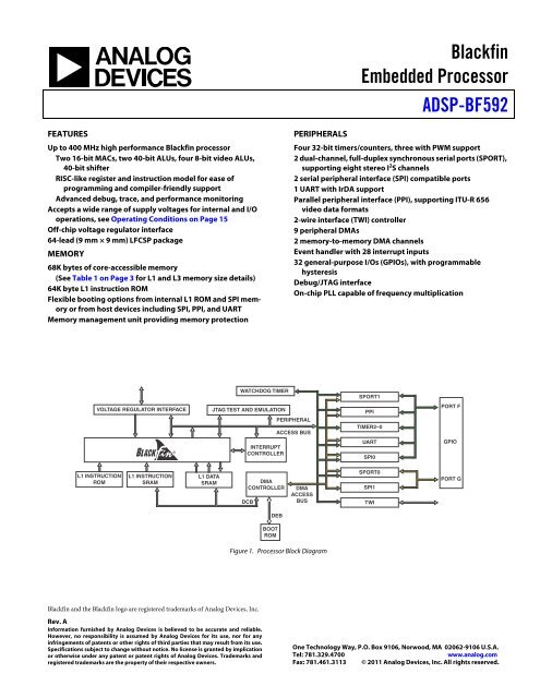
Figure 1. Processor Block Diagram<br />
Blackfin<br />
Embedded Processor<br />
<strong>ADSP</strong>-<strong>BF592</strong><br />
PERIPHERALS<br />
Four 32-bit timers/counters, three with PWM support<br />
2 dual-channel, full-duplex synchronous serial ports (SPORT),<br />
supporting eight stereo I2S channels<br />
2 serial peripheral interface (SPI) compatible ports<br />
1 UART with IrDA support<br />
Parallel peripheral interface (PPI), supporting ITU-R 656<br />
video data formats<br />
2-wire interface (TWI) controller<br />
9 peripheral DMAs<br />
2 memory-to-memory DMA channels<br />
Event handler with 28 interrupt inputs<br />
32 general-purpose I/Os (GPIOs), with programmable<br />
hysteresis<br />
Debug/JTAG interface<br />
On-chip PLL capable of frequency multiplication<br />
ACCESS BUS<br />
DEB<br />
DMA<br />
ACCESS<br />
BUS<br />
SPORT1<br />
PPI<br />
TIMER2–0<br />
UART<br />
SPI0<br />
SPORT0<br />
SPI1<br />
TWI<br />
PORT F<br />
GPIO<br />
PORT G<br />
One Technology Way, P.O. Box 9106, Norwood, MA 02062-9106 U.S.A.<br />
Tel: 781.329.4700 www.analog.com<br />
Fax: 781.461.3113 © 2011 <strong>Analog</strong> <strong>Devices</strong>, Inc. All rights reserved.
<strong>ADSP</strong>-<strong>BF592</strong><br />
TABLE OF CONTENTS<br />
Features ................................................................. 1<br />
Memory ................................................................ 1<br />
Peripherals ............................................................. 1<br />
General Description ................................................. 3<br />
Portable Low Power Architecture ............................. 3<br />
System Integration ................................................ 3<br />
Blackfin Processor Core .......................................... 3<br />
Memory Architecture ............................................ 5<br />
Event Handling .................................................... 5<br />
DMA Controllers .................................................. 6<br />
Processor Peripherals ............................................. 6<br />
Dynamic Power Management .................................. 8<br />
Voltage Regulation ................................................ 9<br />
Clock Signals ....................................................... 9<br />
Booting Modes ................................................... 11<br />
Instruction Set Description ................................... 12<br />
Development Tools ............................................. 12<br />
Designing an Emulator-Compatible<br />
Processor Board (Target) ................................... 12<br />
REVISION HISTORY<br />
Rev. 0 to Rev. A<br />
Added 200 MHz model to Electrical Characteristics ....... 17<br />
Added 200 MHz model to Ordering Guide ................... 43<br />
Rev. A | Page 2 of 44 | August 2011<br />
Related Documents .............................................. 12<br />
Related Signal Chains ........................................... 12<br />
Signal Descriptions ................................................. 13<br />
Specifications ........................................................ 15<br />
Operating Conditions ........................................... 15<br />
Electrical Characteristics ....................................... 17<br />
Absolute Maximum Ratings ................................... 19<br />
ESD Sensitivity ................................................... 19<br />
Package Information ............................................ 20<br />
Timing Specifications ........................................... 21<br />
Output Drive Currents ......................................... 35<br />
Test Conditions .................................................. 36<br />
Environmental Conditions .................................... 39<br />
64-Lead LFCSP Lead Assignment ............................... 40<br />
Outline Dimensions ................................................ 42<br />
Automotive Products .............................................. 42<br />
Ordering Guide ..................................................... 42
GENERAL DESCRIPTION<br />
The <strong>ADSP</strong>-<strong>BF592</strong> processor is a member of the Blackfin ® family<br />
of products, incorporating the <strong>Analog</strong> <strong>Devices</strong>/Intel Micro<br />
Signal Architecture (MSA). Blackfin processors combine a dual-<br />
MAC state-of-the-art signal processing engine, the advantages<br />
of a clean, orthogonal RISC-like microprocessor instruction set,<br />
and single-instruction, multiple-data (SIMD) multimedia capabilities<br />
into a single instruction-set architecture.<br />
The <strong>ADSP</strong>-<strong>BF592</strong> processor is completely code compatible with<br />
other Blackfin processors. The <strong>ADSP</strong>-<strong>BF592</strong> processor offers<br />
performance up to 400 MHz and reduced static power consumption.<br />
The processor features are shown in Table 1.<br />
Table 1. Processor Features<br />
Feature <strong>ADSP</strong>-<strong>BF592</strong><br />
Timer/Counters with PWM 3<br />
SPORTs 2<br />
SPIs 2<br />
UART 1<br />
Parallel Peripheral Interface 1<br />
TWI 1<br />
GPIOs 32<br />
L1 Instruction SRAM 32K<br />
L1 Instruction ROM 64K<br />
L1 Data SRAM 32K<br />
L1 Scratchpad SRAM 4K<br />
L3 Boot ROM 4K<br />
Maximum Instruction Rate1 400 MHz<br />
Maximum System Clock Speed 100 MHz<br />
Package Options 64-Lead LFCSP<br />
1 Maximum instruction rate is not available with every possible SCLK selection.<br />
Memory (bytes)<br />
By integrating a rich set of industry-leading system peripherals<br />
and memory, Blackfin processors are the platform of choice for<br />
next-generation applications that require RISC-like programmability,<br />
multimedia support, and leading-edge signal<br />
processing in one integrated package.<br />
PORTABLE LOW POWER ARCHITECTURE<br />
Blackfin processors provide world-class power management<br />
and performance. They are produced with a low power and low<br />
voltage design methodology and feature on-chip dynamic<br />
power management, which provides the ability to vary both the<br />
voltage and frequency of operation to significantly lower overall<br />
power consumption. This capability can result in a substantial<br />
reduction in power consumption, compared with just varying<br />
the frequency of operation. This allows longer battery life for<br />
portable appliances.<br />
head looping. The architecture is fully interlocked, meaning that<br />
the programmer need not manage the pipeline when executing<br />
Rev. A | Page 3 of 44 | August 2011<br />
<strong>ADSP</strong>-<strong>BF592</strong><br />
SYSTEM INTEGRATION<br />
The <strong>ADSP</strong>-<strong>BF592</strong> processor is a highly integrated system-on-achip<br />
solution for the next generation of digital communication<br />
and consumer multimedia applications. By combining industry<br />
standard interfaces with a high performance signal processing<br />
core, cost-effective applications can be developed quickly, without<br />
the need for costly external components. The system<br />
peripherals include a watchdog timer; three 32-bit timers/counters<br />
with PWM support; two dual-channel, full-duplex<br />
synchronous serial ports (SPORTs); two serial peripheral interface<br />
(SPI) compatible ports; one UART ® with IrDA support; a<br />
parallel peripheral interface (PPI); and a 2-wire interface (TWI)<br />
controller.<br />
BLACKFIN PROCESSOR CORE<br />
As shown in Figure 2, the Blackfin processor core contains two<br />
16-bit multipliers, two 40-bit accumulators, two 40-bit ALUs,<br />
four video ALUs, and a 40-bit shifter. The computation units<br />
process 8-, 16-, or 32-bit data from the register file.<br />
The compute register file contains eight 32-bit registers. When<br />
performing compute operations on 16-bit operand data, the<br />
register file operates as 16 independent 16-bit registers. All<br />
operands for compute operations come from the multiported<br />
register file and instruction constant fields.<br />
Each MAC can perform a 16-bit by 16-bit multiply in each<br />
cycle, accumulating the results into the 40-bit accumulators.<br />
Signed and unsigned formats, rounding, and saturation<br />
are supported.<br />
The ALUs perform a traditional set of arithmetic and logical<br />
operations on 16-bit or 32-bit data. In addition, many special<br />
instructions are included to accelerate various signal processing<br />
tasks. These include bit operations such as field extract and population<br />
count, modulo 232 multiply, divide primitives, saturation<br />
and rounding, and sign/exponent detection. The set of video<br />
instructions includes byte alignment and packing operations,<br />
16-bit and 8-bit adds with clipping, 8-bit average operations,<br />
and 8-bit subtract/absolute value/accumulate (SAA) operations.<br />
The compare/select and vector search instructions are also<br />
provided.<br />
For certain instructions, two 16-bit ALU operations can be performed<br />
simultaneously on register pairs (a 16-bit high half and<br />
16-bit low half of a compute register). If the second ALU is used,<br />
quad 16-bit operations are possible.<br />
The 40-bit shifter can perform shifts and rotates and is used to<br />
support normalization, field extract, and field deposit<br />
instructions.<br />
The program sequencer controls the flow of instruction execution,<br />
including instruction alignment and decoding. For<br />
program flow control, the sequencer supports PC relative and<br />
indirect conditional jumps (with static branch prediction) and<br />
subroutine calls. Hardware is provided to support zero over<br />
instructions with data dependencies.
<strong>ADSP</strong>-<strong>BF592</strong><br />
The address arithmetic unit provides two addresses for simultaneous<br />
dual fetches from memory. It contains a multiported<br />
register file consisting of four sets of 32-bit index, modify,<br />
length, and base registers (for circular buffering) and eight<br />
additional 32-bit pointer registers (for C-style indexed stack<br />
manipulation).<br />
Blackfin processors support a modified Harvard architecture in<br />
combination with a hierarchical memory structure. Level 1 (L1)<br />
memories are those that typically operate at the full processor<br />
speed with little or no latency. At the L1 level, the instruction<br />
memory holds instructions only. Data memory holds data, and<br />
a dedicated scratchpad data memory stores stack and local variable<br />
information.<br />
Multiple L1 memory blocks are provided. The memory<br />
management unit (MMU) provides memory protection for<br />
individual tasks that may be operating on the core and can<br />
protect system registers from unintended access.<br />
TO MEMORY<br />
DA1<br />
DA0<br />
SD<br />
LD1<br />
LD0<br />
32<br />
32<br />
32<br />
32<br />
32<br />
R7.H<br />
R6.H<br />
R5.H<br />
R4.H<br />
R3.H<br />
R2.H<br />
R1.H<br />
R0.H<br />
I3<br />
I2<br />
I1<br />
I0<br />
32<br />
RAB<br />
32<br />
R7.L<br />
R6.L<br />
R5.L<br />
R4.L<br />
R3.L<br />
R2.L<br />
R1.L<br />
R0.L<br />
L3<br />
L2<br />
L1<br />
L0<br />
32<br />
B3<br />
B2<br />
B1<br />
B0<br />
16 16<br />
8 8<br />
8 8<br />
BARREL<br />
SHIFTER<br />
ADDRESS ARITHMETIC UNIT<br />
M3<br />
M2<br />
M1<br />
M0<br />
32<br />
Figure 2. Blackfin Processor Core<br />
Rev. A | Page 4 of 44 | August 2011<br />
The architecture provides three modes of operation: user mode,<br />
supervisor mode, and emulation mode. User mode has<br />
restricted access to certain system resources, thus providing a<br />
protected software environment, while supervisor mode has<br />
unrestricted access to the system and core resources.<br />
The Blackfin processor instruction set has been optimized so<br />
that 16-bit opcodes represent the most frequently used instructions,<br />
resulting in excellent compiled code density. Complex<br />
DSP instructions are encoded into 32-bit opcodes, representing<br />
fully featured multifunction instructions. Blackfin processors<br />
support a limited multi-issue capability, where a 32-bit instruction<br />
can be issued in parallel with two 16-bit instructions,<br />
allowing the programmer to use many of the core resources in a<br />
single instruction cycle.<br />
The Blackfin processor assembly language uses an algebraic syntax<br />
for ease of coding and readability. The architecture has been<br />
optimized for use in conjunction with the C/C++ compiler,<br />
resulting in fast and efficient software implementations.<br />
40 40<br />
40 40<br />
A0 A1<br />
32<br />
DAG1<br />
DATA ARITHMETIC UNIT<br />
DAG0<br />
SP<br />
FP<br />
P5<br />
P4<br />
P3<br />
P2<br />
P1<br />
P0<br />
ASTAT<br />
32<br />
PREG<br />
SEQUENCER<br />
ALIGN<br />
DECODE<br />
LOOP BUFFER<br />
CONTROL<br />
UNIT
MEMORY ARCHITECTURE<br />
The Blackfin processor views memory as a single unified<br />
4G byte address space, using 32-bit addresses. All resources,<br />
including internal memory and I/O control registers, occupy<br />
separate sections of this common address space. See Figure 3.<br />
The core-accessible L1 memory system is high performance<br />
internal memory that operates at the core clock frequency. The<br />
external bus interface unit (EBIU) provides access to the boot<br />
ROM.<br />
The memory DMA controller provides high bandwidth datamovement<br />
capability. It can perform block transfers of code or<br />
data between the L1 Instruction SRAM and L1 Data SRAM<br />
memory spaces.<br />
0xFFFF FFFF<br />
0xFFE0 0000<br />
0xFFC0 0000<br />
0xFFB0 1000<br />
0xFFB0 0000<br />
0xFFA2 0000<br />
0xFFA1 0000<br />
0xFFA0 8000<br />
0xFFA0 4000<br />
0xFFA0 0000<br />
0xFF80 8000<br />
0xFF80 0000<br />
0xEF00 1000<br />
0xEF00 0000<br />
0x0000 0000<br />
CORE MEMORY MAPPED REGISTERS (2M BYTES)<br />
SYSTEM MEMORY MAPPED REGISTERS (2M BYTES)<br />
RESERVED<br />
L1 SCRATCHPAD RAM (4K BYTES)<br />
RESERVED<br />
L1 INSTRUCTION ROM (64K BYTES)<br />
RESERVED<br />
L1 INSTRUCTION BANK B SRAM (16K BYTES)<br />
L1 INSTRUCTION BANK A SRAM (16K BYTES)<br />
RESERVED<br />
DATA SRAM (32K BYTES)<br />
RESERVED<br />
BOOT ROM (4K BYTES)<br />
RESERVED<br />
Figure 3. Internal/External Memory Map<br />
Internal (Core-Accessible) Memory<br />
The processor has three blocks of core-accessible memory, providing<br />
high bandwidth access to the core.<br />
The first block is the L1 instruction memory, consisting of<br />
32K bytes SRAM. This memory is accessed at full processor<br />
speed.<br />
The second core-accessible memory block is the L1 data memory,<br />
consisting of 32K bytes. This memory block is accessed at<br />
full processor speed.<br />
The third memory block is a 4K byte L1 scratchpad SRAM,<br />
which runs at the same speed as the other L1 memories.<br />
L1 Utility ROM<br />
The L1 instruction ROM contains utility ROM code. This<br />
includes the TMK (VDK core), C run-time libraries, and DSP<br />
libraries. See the VisualDSP++ documentation for more<br />
information.<br />
Rev. A | Page 5 of 44 | August 2011<br />
<strong>ADSP</strong>-<strong>BF592</strong><br />
Custom ROM (Optional)<br />
The on-chip L1 Instruction ROM on the <strong>ADSP</strong>-<strong>BF592</strong> may be<br />
customized to contain user code with the following features:<br />
• 64K bytes of L1 Instruction ROM available for custom code<br />
• Ability to restrict access to all or specific segments of the<br />
on-chip ROM<br />
Customers wishing to customize the on-chip ROM for their<br />
own application needs should contact ADI sales for more information<br />
on terms and conditions and details on the technical<br />
implementation.<br />
I/O Memory Space<br />
The processor does not define a separate I/O space. All<br />
resources are mapped through the flat 32-bit address space.<br />
On-chip I/O devices have their control registers mapped into<br />
memory-mapped registers (MMRs) at addresses near the top of<br />
the 4G byte address space. These are separated into two smaller<br />
blocks, one which contains the control MMRs for all core functions,<br />
and the other which contains the registers needed for<br />
setup and control of the on-chip peripherals outside of the core.<br />
The MMRs are accessible only in supervisor mode and appear<br />
as reserved space to on-chip peripherals.<br />
Booting from ROM<br />
The processor contains a small on-chip boot kernel, which configures<br />
the appropriate peripheral for booting. If the processor is<br />
configured to boot from boot ROM memory space, the processor<br />
starts executing from the on-chip boot ROM. For more<br />
information, see Booting Modes on Page 11.<br />
EVENT HANDLING<br />
The event controller on the processor handles all asynchronous<br />
and synchronous events to the processor. The processor<br />
provides event handling that supports both nesting and prioritization.<br />
Nesting allows multiple event service routines to be<br />
active simultaneously. Prioritization ensures that servicing of a<br />
higher-priority event takes precedence over servicing of a lowerpriority<br />
event. The controller provides support for five different<br />
types of events:<br />
• Emulation – An emulation event causes the processor to<br />
enter emulation mode, allowing command and control of<br />
the processor via the JTAG interface.<br />
• RESET – This event resets the processor.<br />
• Nonmaskable Interrupt (NMI) – The NMI event can be<br />
generated by the software watchdog timer or by the NMI<br />
input signal to the processor. The NMI event is frequently<br />
used as a power-down indicator to initiate an orderly shutdown<br />
of the system.
<strong>ADSP</strong>-<strong>BF592</strong><br />
• Exceptions – Events that occur synchronously to program<br />
flow (in other words, the exception is taken before the<br />
instruction is allowed to complete). Conditions such as<br />
data alignment violations and undefined instructions cause<br />
exceptions.<br />
• Interrupts – Events that occur asynchronously to program<br />
flow. They are caused by input signals, timers, and other<br />
peripherals, as well as by an explicit software instruction.<br />
Each event type has an associated register to hold the return<br />
address and an associated return-from-event instruction. When<br />
an event is triggered, the state of the processor is saved on the<br />
supervisor stack.<br />
The processor event controller consists of two stages: the core<br />
event controller (CEC) and the system interrupt controller<br />
(SIC). The core event controller works with the system interrupt<br />
controller to prioritize and control all system events. Conceptually,<br />
interrupts from the peripherals enter into the SIC and are<br />
then routed directly into the general-purpose interrupts of the<br />
CEC.<br />
Core Event Controller (CEC)<br />
The CEC supports nine general-purpose interrupts (IVG15–7),<br />
in addition to the dedicated interrupt and exception events. Of<br />
these general-purpose interrupts, the two lowest priority<br />
interrupts (IVG15–14) are recommended to be reserved for<br />
software interrupt handlers, leaving seven prioritized interrupt<br />
inputs to support the peripherals of the processor. The inputs to<br />
the CEC, their names in the event vector table (EVT), and their<br />
priorities are described in the <strong>ADSP</strong>-BF59x Blackfin Processor<br />
Hardware Reference, “System Interrupts” chapter.<br />
System Interrupt Controller (SIC)<br />
The system interrupt controller provides the mapping and routing<br />
of events from the many peripheral interrupt sources to the<br />
prioritized general-purpose interrupt inputs of the CEC.<br />
Although the processor provides a default mapping, the user<br />
can alter the mappings and priorities of interrupt events by writing<br />
the appropriate values into the interrupt assignment<br />
registers (SIC_IARx). The inputs into the SIC and the default<br />
mappings into the CEC are described in the <strong>ADSP</strong>-BF59x Blackfin<br />
Processor Hardware Reference, “System Interrupts” chapter.<br />
The SIC allows further control of event processing by providing<br />
three pairs of 32-bit interrupt control and status registers. Each<br />
register contains a bit, corresponding to each peripheral interrupt<br />
event. For more information, see the <strong>ADSP</strong>-BF59x Blackfin<br />
Processor Hardware Reference, “System Interrupts” chapter.<br />
DMA CONTROLLERS<br />
The processor has multiple, independent DMA channels that<br />
support automated data transfers with minimal overhead for<br />
the processor core. DMA transfers can occur between the processor’s<br />
internal memories and any of its DMA-capable<br />
peripherals. DMA-capable peripherals include the SPORTs, SPI<br />
ports, UART, and PPI. Each individual DMA-capable peripheral<br />
has at least one dedicated DMA channel.<br />
Rev. A | Page 6 of 44 | August 2011<br />
The processor DMA controller supports both one-dimensional<br />
(1-D) and two-dimensional (2-D) DMA transfers. DMA transfer<br />
initialization can be implemented from registers or from sets<br />
of parameters called descriptor blocks.<br />
The 2-D DMA capability supports arbitrary row and column<br />
sizes up to 64K elements by 64K elements, and arbitrary row<br />
and column step sizes up to ±32K elements. Furthermore, the<br />
column step size can be less than the row step size, allowing<br />
implementation of interleaved data streams. This feature is<br />
especially useful in video applications where data can be deinterleaved<br />
on the fly.<br />
Examples of DMA types supported by the processor DMA controller<br />
include:<br />
• A single, linear buffer that stops upon completion<br />
• A circular, auto-refreshing buffer that interrupts on each<br />
full or fractionally full buffer<br />
• 1-D or 2-D DMA using a linked list of descriptors<br />
• 2-D DMA using an array of descriptors, specifying only the<br />
base DMA address within a common page<br />
In addition to the dedicated peripheral DMA channels, there are<br />
two memory DMA channels, which are provided for transfers<br />
between the various memories of the processor system with<br />
minimal processor intervention. Memory DMA transfers can be<br />
controlled by a very flexible descriptor-based methodology or<br />
by a standard register-based autobuffer mechanism.<br />
PROCESSOR PERIPHERALS<br />
The <strong>ADSP</strong>-<strong>BF592</strong> processor contains a rich set of peripherals<br />
connected to the core via several high bandwidth buses, providing<br />
flexibility in system configuration, as well as excellent<br />
overall system performance (see Figure 1). The processor also<br />
contains dedicated communication modules and high speed<br />
serial and parallel ports, an interrupt controller for flexible management<br />
of interrupts from the on-chip peripherals or external<br />
sources, and power management control functions to tailor the<br />
performance and power characteristics of the processor and system<br />
to many application scenarios.<br />
The SPORTs, SPIs, UART, and PPI peripherals are supported<br />
by a flexible DMA structure. There are also separate memory<br />
DMA channels dedicated to data transfers between the processor’s<br />
various memory spaces, including boot ROM. Multiple<br />
on-chip buses running at up to 100 MHz provide enough bandwidth<br />
to keep the processor core running along with activity on<br />
all of the on-chip and external peripherals.<br />
The <strong>ADSP</strong>-<strong>BF592</strong> processor includes an interface to an off-chip<br />
voltage regulator in support of the processor’s dynamic power<br />
management capability.<br />
Watchdog Timer<br />
The processor includes a 32-bit timer that can be used to implement<br />
a software watchdog function. A software watchdog can<br />
improve system availability by forcing the processor to a known<br />
state through generation of a hardware reset, nonmaskable<br />
interrupt (NMI), or general-purpose interrupt, if the timer<br />
expires before being reset by software. The programmer
initializes the count value of the timer, enables the appropriate<br />
interrupt, then enables the timer. Thereafter, the software must<br />
reload the counter before it counts to zero from the programmed<br />
value. This protects the system from remaining in an<br />
unknown state where software, which would normally reset the<br />
timer, has stopped running due to an external noise condition<br />
or software error.<br />
If configured to generate a hardware reset, the watchdog timer<br />
resets both the core and the processor peripherals. After a reset,<br />
software can determine whether the watchdog was the source of<br />
the hardware reset by interrogating a status bit in the watchdog<br />
timer control register.<br />
The timer is clocked by the system clock (SCLK) at a maximum<br />
frequency of fSCLK. Timers<br />
There are four general-purpose programmable timer units in<br />
the processor. Three timers have an external pin that can be<br />
configured either as a pulse width modulator (PWM) or timer<br />
output, as an input to clock the timer, or as a mechanism for<br />
measuring pulse widths and periods of external events. These<br />
timers can be synchronized to an external clock input to the several<br />
other associated PF pins, to an external clock input to the<br />
PPI_CLK input pin, or to the internal SCLK.<br />
The timer units can be used in conjunction with the UART to<br />
measure the width of the pulses in the data stream to provide a<br />
software auto-baud detect function for the respective serial<br />
channels.<br />
The timers can generate interrupts to the processor core providing<br />
periodic events for synchronization, either to the system<br />
clock or to a count of external signals.<br />
In addition to the three general-purpose programmable timers,<br />
a fourth timer is also provided. This extra timer is clocked by the<br />
internal processor clock and is typically used as a system tick<br />
clock for generation of operating system periodic interrupts.<br />
Serial Ports<br />
The <strong>ADSP</strong>-<strong>BF592</strong> processor incorporates two dual-channel<br />
synchronous serial ports (SPORT0 and SPORT1) for serial and<br />
multiprocessor communications. The SPORTs support the following<br />
features:<br />
Serial port data can be automatically transferred to and from<br />
on-chip memory/external memory via dedicated DMA channels.<br />
Each of the serial ports can work in conjunction with<br />
another serial port to provide TDM support. In this configuration,<br />
one SPORT provides two transmit signals while the other<br />
SPORT provides the two receive signals. The frame sync and<br />
clock are shared.<br />
Serial ports operate in five modes:<br />
• Standard DSP serial mode<br />
• Multichannel (TDM) mode<br />
• I2S mode<br />
• Packed I2S mode<br />
• Left-justified mode<br />
Rev. A | Page 7 of 44 | August 2011<br />
<strong>ADSP</strong>-<strong>BF592</strong><br />
Serial Peripheral Interface (SPI) Ports<br />
The processor has two SPI-compatible ports that enable the<br />
processor to communicate with multiple SPI-compatible<br />
devices.<br />
The SPI interface uses three pins for transferring data: two data<br />
pins (Master Output-Slave Input, MOSI, and Master Input-<br />
Slave Output, MISO) and a clock pin (serial clock, SCK). An SPI<br />
chip select input pin (SPIx_SS) lets other SPI devices select the<br />
processor, and many SPI chip select output pins (SPIx_SEL7–1)<br />
let the processor select other SPI devices. The SPI select pins are<br />
reconfigured general-purpose I/O pins. Using these pins, the<br />
SPI port provides a full-duplex, synchronous serial interface,<br />
which supports both master/slave modes and multimaster<br />
environments.<br />
UART Port<br />
The <strong>ADSP</strong>-<strong>BF592</strong> processor provides a full-duplex universal<br />
asynchronous receiver/transmitter (UART) port, which is fully<br />
compatible with PC-standard UARTs. The UART port provides<br />
a simplified UART interface to other peripherals or hosts,<br />
supporting full-duplex, DMA-supported, asynchronous transfers<br />
of serial data. The UART port includes support for five to<br />
eight data bits, one or two stop bits, and none, even, or odd parity.<br />
The UART port supports two modes of operation:<br />
• PIO (programmed I/O) – The processor sends or receives<br />
data by writing or reading I/O mapped UART registers.<br />
The data is double-buffered on both transmit and receive.<br />
• DMA (direct memory access) – The DMA controller transfers<br />
both transmit and receive data. This reduces the<br />
number and frequency of interrupts required to transfer<br />
data to and from memory. The UART has two dedicated<br />
DMA channels, one for transmit and one for receive. These<br />
DMA channels have lower default priority than most DMA<br />
channels because of their relatively low service rates.<br />
Parallel Peripheral Interface (PPI)<br />
The processor provides a parallel peripheral interface (PPI) that<br />
can connect directly to parallel analog-to-digital and digital-toanalog<br />
converters, video encoders and decoders, and other general-purpose<br />
peripherals. The PPI consists of a dedicated input<br />
clock pin, up to three frame synchronization pins, and up to 16<br />
data pins. The input clock supports parallel data rates up to half<br />
the system clock rate, and the synchronization signals can be<br />
configured as either inputs or outputs.<br />
The PPI supports a variety of general-purpose and ITU-R 656<br />
modes of operation. In general-purpose mode, the PPI provides<br />
half-duplex, bidirectional data transfer with up to 16 bits of<br />
data. Up to three frame synchronization signals are also provided.<br />
In ITU-R 656 mode, the PPI provides half-duplex<br />
bidirectional transfer of 8- or 10-bit video data. Additionally,<br />
on-chip decode of embedded start-of-line (SOL) and start-offield<br />
(SOF) preamble packets is supported.
<strong>ADSP</strong>-<strong>BF592</strong><br />
General-Purpose Mode Descriptions<br />
The general-purpose modes of the PPI are intended to suit a<br />
wide variety of data capture and transmission applications.<br />
Three distinct submodes are supported:<br />
• Input mode – Frame syncs and data are inputs into the PPI.<br />
Input mode is intended for ADC applications, as well as<br />
video communication with hardware signaling.<br />
• Frame capture mode – Frame syncs are outputs from the<br />
PPI, but data are inputs. This mode allows the video<br />
source(s) to act as a slave (for frame capture for example).<br />
• Output mode – Frame syncs and data are outputs from the<br />
PPI. Output mode is used for transmitting video or other<br />
data with up to three output frame syncs.<br />
ITU-R 656 Mode Descriptions<br />
The ITU-R 656 modes of the PPI are intended to suit a wide<br />
variety of video capture, processing, and transmission applications.<br />
Three distinct submodes are supported:<br />
• Active video only mode – Active video only mode is used<br />
when only the active video portion of a field is of interest<br />
and not any of the blanking intervals.<br />
• Vertical blanking only mode – In this mode, the PPI only<br />
transfers vertical blanking interval (VBI) data.<br />
• Entire field mode – In this mode, the entire incoming bit<br />
stream is read in through the PPI.<br />
TWI Controller Interface<br />
The processor includes a 2-wire interface (TWI) module for<br />
providing a simple exchange method of control data between<br />
multiple devices. The TWI is functionally compatible with the<br />
widely used I 2 C ® bus standard. The TWI module offers the<br />
capabilities of simultaneous master and slave operation and<br />
support for both 7-bit addressing and multimedia data arbitration.<br />
The TWI interface utilizes two pins for transferring clock<br />
(SCL) and data (SDA) and supports the protocol at speeds up to<br />
400K bits/sec.<br />
The TWI module is compatible with serial camera control bus<br />
(SCCB) functionality for easier control of various CMOS camera<br />
sensor devices.<br />
Ports<br />
The processor groups the many peripheral signals to two<br />
ports—Port F and Port G. Most of the associated pins are shared<br />
by multiple signals. The ports function as multiplexer controls.<br />
General-Purpose I/O (GPIO)<br />
The processor has 32 bidirectional, general-purpose I/O (GPIO)<br />
pins allocated across two separate GPIO modules—PORTFIO<br />
and PORTGIO, associated with Port F and Port G respectively.<br />
Each GPIO-capable pin shares functionality with other processor<br />
peripherals via a multiplexing scheme; however, the GPIO<br />
functionality is the default state of the device upon power-up.<br />
Neither GPIO output nor input drivers are active by default.<br />
Each general-purpose port pin can be individually controlled by<br />
manipulation of the port control, status, and interrupt registers.<br />
Rev. A | Page 8 of 44 | August 2011<br />
DYNAMIC POWER MANAGEMENT<br />
The processor provides five operating modes, each with a different<br />
performance/power profile. In addition, dynamic power<br />
management provides the control functions to dynamically alter<br />
the processor core supply voltage, further reducing power dissipation.<br />
When configured for a 0 V core supply voltage, the<br />
processor enters the hibernate state. Control of clocking to each<br />
of the processor peripherals also reduces power consumption.<br />
See Table 2 for a summary of the power settings for each mode.<br />
Table 2. Power Settings<br />
Core System<br />
PLL Clock Clock Core<br />
Mode/State PLL Bypassed (CCLK) (SCLK) Power<br />
Full On Enabled No Enabled Enabled On<br />
Active Enabled/<br />
Disabled<br />
Yes Enabled Enabled On<br />
Sleep Enabled — Disabled Enabled On<br />
Deep Sleep Disabled — Disabled Disabled On<br />
Hibernate Disabled — Disabled Disabled Off<br />
Full-On Operating Mode—Maximum Performance<br />
In the full-on mode, the PLL is enabled and is not bypassed,<br />
providing capability for maximum operational frequency. This<br />
is the power-up default execution state in which maximum performance<br />
can be achieved. The processor core and all enabled<br />
peripherals run at full speed.<br />
Active Operating Mode—Moderate Dynamic Power<br />
Savings<br />
In the active mode, the PLL is enabled but bypassed. Because the<br />
PLL is bypassed, the processor’s core clock (CCLK) and system<br />
clock (SCLK) run at the input clock (CLKIN) frequency. DMA<br />
access is available to appropriately configured L1 memories.<br />
For more information about PLL controls, see the “Dynamic<br />
Power Management” chapter in the <strong>ADSP</strong>-BF59x Blackfin Processor<br />
Hardware Reference.<br />
Sleep Operating Mode—High Dynamic Power Savings<br />
The sleep mode reduces dynamic power dissipation by disabling<br />
the clock to the processor core (CCLK). The PLL and system<br />
clock (SCLK), however, continue to operate in this mode. Typically,<br />
an external event wakes up the processor.<br />
System DMA access to L1 memory is not supported in<br />
sleep mode.<br />
Deep Sleep Operating Mode—Maximum Dynamic Power<br />
Savings<br />
The deep sleep mode maximizes dynamic power savings by disabling<br />
the clocks to the processor core (CCLK) and to all<br />
synchronous peripherals (SCLK). Asynchronous peripherals<br />
may still be running but cannot access internal resources or<br />
external memory. This powered-down mode can only be exited<br />
by assertion of the reset interrupt (RESET) or by an asynchronous<br />
interrupt generated by a GPIO pin.
Note that when a GPIO pin is used to trigger wake from deep<br />
sleep, the programmed wake level must linger for at least 10ns<br />
to guarantee detection.<br />
Hibernate State—Maximum Static Power Savings<br />
The hibernate state maximizes static power savings by disabling<br />
clocks to the processor core (CCLK) and to all of the peripherals<br />
(SCLK), as well as signaling an external voltage regulator that<br />
VDDINT can be shut off. Any critical information stored internally<br />
(for example, memory contents, register contents, and<br />
other information) must be written to a nonvolatile storage<br />
device prior to removing power if the processor state is to be<br />
preserved. Writing b#0 to the HIBERNATE bit causes<br />
EXT_WAKE to transition low, which can be used to signal an<br />
external voltage regulator to shut down.<br />
Since VDDEXT can still be supplied in this mode, all of the external<br />
pins three-state, unless otherwise specified. This allows<br />
other devices that may be connected to the processor to still<br />
have power applied without drawing unwanted current.<br />
As long as VDDEXT is applied, the VR_CTL register maintains its<br />
state during hibernation. All other internal registers and memories,<br />
however, lose their content in the hibernate state.<br />
Power Savings<br />
As shown in Table 3, the processor supports two different<br />
power domains, which maximizes flexibility while maintaining<br />
compliance with industry standards and conventions. By isolating<br />
the internal logic of the processor into its own power<br />
domain, separate from other I/O, the processor can take advantage<br />
of dynamic power management without affecting the other<br />
I/O devices. There are no sequencing requirements for the<br />
various power domains, but all domains must be powered<br />
according to the appropriate Specifications table for processor<br />
operating conditions, even if the feature/peripheral is not used.<br />
Table 3. Power Domains<br />
Power Domain VDD Range<br />
All internal logic and memories VDDINT All other I/O VDDEXT The dynamic power management feature of the processor<br />
allows both the processor’s input voltage (VDDINT) and clock frequency<br />
(fCCLK) to be dynamically controlled.<br />
The power dissipated by a processor is largely a function of its<br />
clock frequency and the square of the operating voltage. For<br />
example, reducing the clock frequency by 25% results in a 25%<br />
reduction in dynamic power dissipation, while reducing the<br />
voltage by 25% reduces dynamic power dissipation by more<br />
than 40%. Further, these power savings are additive, in that if<br />
the clock frequency and supply voltage are both reduced, the<br />
power savings can be dramatic, as shown in the following<br />
equations.<br />
Power Savings Factor<br />
fCCLKRED ------------------fCCLKNOM<br />
Rev. A | Page 9 of 44 | August 2011<br />
=<br />
where:<br />
fCCLKNOM is the nominal core clock frequency<br />
fCCLKRED is the reduced core clock frequency<br />
VDDINTNOM is the nominal internal supply voltage<br />
VDDINTRED is the reduced internal supply voltage<br />
TNOM is the duration running at fCCLKNOM TRED is the duration running at fCCLKRED <strong>ADSP</strong>-<strong>BF592</strong><br />
VOLTAGE REGULATION<br />
The <strong>ADSP</strong>-<strong>BF592</strong> processor requires an external voltage regulator<br />
to power the VDDINT domain. To reduce standby power<br />
consumption, the external voltage regulator can be signaled<br />
through EXT_WAKE to remove power from the processor core.<br />
This signal is high-true for power-up and may be connected<br />
directly to the low-true shut-down input of many common<br />
regulators.<br />
While in the hibernate state, the external supply, VDDEXT, can<br />
still be applied, eliminating the need for external buffers. The<br />
external voltage regulator can be activated from this powerdown<br />
state by asserting the RESET pin, which then initiates a<br />
boot sequence. EXT_WAKE indicates a wakeup to the external<br />
voltage regulator.<br />
The power good (PG) input signal allows the processor to start<br />
only after the internal voltage has reached a chosen level. In this<br />
way, the startup time of the external regulator is detected after<br />
hibernation. For a complete description of the power-good<br />
functionality, refer to the <strong>ADSP</strong>-BF59x Blackfin Processor Hardware<br />
Reference.<br />
CLOCK SIGNALS<br />
VDDINTRED ------------------------<br />
VDDINTNOM TRED TNOM <br />
<br />
2<br />
×<br />
× -----------<br />
<br />
<br />
% Power Savings =<br />
( 1 – Power Savings Factor)<br />
× 100%<br />
The processor can be clocked by an external crystal, a sine wave<br />
input, or a buffered, shaped clock derived from an external<br />
clock oscillator.<br />
If an external clock is used, it should be a TTL-compatible signal<br />
and must not be halted, changed, or operated below the specified<br />
frequency during normal operation. This signal is<br />
connected to the processor’s CLKIN pin. When an external<br />
clock is used, the XTAL pin must be left unconnected.<br />
Alternatively, because the processor includes an on-chip oscillator<br />
circuit, an external crystal may be used. For fundamental<br />
frequency operation, use the circuit shown in Figure 4. A<br />
parallel -resonant, fundamental frequency, microprocessorgrade<br />
crystal is connected across the CLKIN and XTAL pins.<br />
The on-chip resistance between CLKIN and the XTAL pin is in
<strong>ADSP</strong>-<strong>BF592</strong><br />
the 500 kΩ range. Further parallel resistors are typically not recommended.<br />
The two capacitors and the series resistor shown in<br />
Figure 4 fine tune phase and amplitude of the sine frequency.<br />
The capacitor and resistor values shown in Figure 4 are typical<br />
values only. The capacitor values are dependent upon the crystal<br />
manufacturers’ load capacitance recommendations and the PCB<br />
physical layout. The resistor value depends on the drive level<br />
specified by the crystal manufacturer. The user should verify the<br />
customized values based on careful investigations on multiple<br />
devices over temperature range.<br />
EN<br />
EXTCLK<br />
SELECT<br />
EN<br />
BLACKFIN<br />
CLKBUF<br />
CLKIN<br />
18 pF *<br />
CLKOUT (SCLK)<br />
TO PLL CIRCUITRY<br />
330 *<br />
560 <br />
XTAL<br />
18 pF *<br />
Figure 4. External Crystal Connections<br />
FOR OVERTONE<br />
OPERATION ONLY:<br />
NOTE: VALUES MARKED WITH * MUST BE CUSTOMIZED, DEPENDING<br />
ON THE CRYSTAL AND LAYOUT. PLEASE ANALYZE CAREFULLY. FOR<br />
FREQUENCIES ABOVE 33 MHz, THE SUGGESTED CAPACITOR VALUE<br />
OF 18 pF SHOULD BE TREATED AS A MAXIMUM, AND THE SUGGESTED<br />
RESISTOR VALUE SHOULD BE REDUCED TO 0 .<br />
A third-overtone crystal can be used for frequencies above<br />
25 MHz. The circuit is then modified to ensure crystal operation<br />
only at the third overtone, by adding a tuned inductor circuit as<br />
shown in Figure 4. A design procedure for third-overtone operation<br />
is discussed in detail in (EE-168) Using Third Overtone<br />
Crystals with the <strong>ADSP</strong>-218x DSP on the <strong>Analog</strong> <strong>Devices</strong> website<br />
(www.analog.com)—use site search on “EE-168.”<br />
The Blackfin core runs at a different clock rate than the on-chip<br />
peripherals. As shown in Figure 5, the core clock (CCLK) and<br />
system peripheral clock (SCLK) are derived from the input<br />
clock (CLKIN) signal. An on-chip PLL is capable of multiplying<br />
the CLKIN signal by a programmable 5× to 64× multiplication<br />
factor (bounded by specified minimum and maximum VCO<br />
frequencies). The default multiplier is 6×, but it can be modified<br />
by a software instruction sequence.<br />
On-the-fly frequency changes can be effected by simply writing<br />
to the PLL_DIV register. The maximum allowed CCLK and<br />
SCLK rates depend on the applied voltages VDDINT and VDDEXT; the VCO is always permitted to run up to the frequency specified<br />
by the part’s instruction rate. The EXTCLK pin can be<br />
configured to output either the SCLK frequency or the input<br />
buffered CLKIN frequency, called CLKBUF. When configured<br />
to output SCLK (CLKOUT), the EXTCLK pin acts as a reference<br />
signal in many timing specifications. While three-stated by<br />
default, it can be enabled using the VRCTL register.<br />
CLKIN<br />
Rev. A | Page 10 of 44 | August 2011<br />
Figure 5. Frequency Modification Methods<br />
All on-chip peripherals are clocked by the system clock (SCLK).<br />
The system clock frequency is programmable by means of the<br />
SSEL3–0 bits of the PLL_DIV register. The values programmed<br />
into the SSEL fields define a divide ratio between the PLL output<br />
(VCO) and the system clock. SCLK divider values are 1 through<br />
15. Table 4 illustrates typical system clock ratios.<br />
Note that the divisor ratio must be chosen to limit the system<br />
clock frequency to its maximum of fSCLK. The SSEL value can be<br />
changed dynamically without any PLL lock latencies by writing<br />
the appropriate values to the PLL divisor register (PLL_DIV).<br />
The core clock (CCLK) frequency can also be dynamically<br />
changed by means of the CSEL1–0 bits of the PLL_DIV register.<br />
Supported CCLK divider ratios are 1, 2, 4, and 8, as shown in<br />
Table 5. This programmable core clock capability is useful for<br />
fast core frequency modifications.<br />
Table 5. Core Clock Ratios<br />
Signal Name<br />
CSEL1–0<br />
Table 4. Example System Clock Ratios<br />
Signal Name<br />
SSEL3–0<br />
“FINE” ADJUSTMENT<br />
REQUIRES PLL SEQUENCING<br />
PLL<br />
5 to 64<br />
Divider Ratio<br />
VCO/CCLK<br />
Divider Ratio<br />
VCO/SCLK<br />
VCO<br />
SCLK CCLK<br />
“COARSE” ADJUSTMENT<br />
ON-THE-FLY<br />
÷ 1, 2, 4, 8<br />
÷ 1 to 15<br />
Example Frequency Ratios<br />
(MHz)<br />
VCO CCLK<br />
00 1:1 300 300<br />
01 2:1 300 150<br />
10 4:1 400 100<br />
11 8:1 200 25<br />
Example Frequency Ratios<br />
(MHz)<br />
VCO SCLK<br />
0010 2:1 100 50<br />
0110 6:1 300 50<br />
1010 10:1 400 40<br />
CCLK<br />
SCLK<br />
The maximum CCLK frequency both depends on the part’s<br />
instruction rate (see Page Page 43) and depends on the applied<br />
V DDINT voltage. See Table 8 for details. The maximal system<br />
clock rate (SCLK) depends on the chip package and the applied<br />
VDDINT and VDDEXT voltages (see Table 10).
BOOTING MODES<br />
The processor has several mechanisms (listed in Table 6) for<br />
automatically loading internal and external memory after a<br />
reset. The boot mode is defined by the BMODE input pins dedicated<br />
to this purpose. There are two categories of boot modes.<br />
In master boot modes, the processor actively loads data from<br />
parallel or serial memories. In slave boot modes, the processor<br />
receives data from external host devices.<br />
Table 6. Booting Modes<br />
BMODE2–0 Description<br />
000 Idle/No Boot<br />
001 Reserved<br />
010 SPI1 master boot from Flash, using SPI1_SSEL5 on PG11<br />
011 SPI1 slave boot from external master<br />
100 SPI0 master boot from Flash, using SPI0_SSEL2 on PF8<br />
101 Boot from PPI port<br />
110 Boot from UART host device<br />
111 Execute from Internal L1 ROM<br />
The boot modes listed in Table 6 provide a number of mechanisms<br />
for automatically loading the processor’s internal and<br />
external memories after a reset. By default, all boot modes use<br />
the slowest meaningful configuration settings. Default settings<br />
can be altered via the initialization code feature at boot time.<br />
The BMODE pins of the reset configuration register, sampled<br />
during power-on resets and software-initiated resets, implement<br />
the modes shown in Table 6.<br />
• IDLE State/No Boot (BMODE - 0x0) — In this mode, the<br />
boot kernel transitions the processor into Idle state. The<br />
processor can then be controlled through JTAG for recovery,<br />
debug, or other functions.<br />
• SPI1 master boot from flash (BMODE = 0x2) — In this<br />
mode, SPI1 is configured to operate in master mode and to<br />
connect to 8-, 16-, 24-, or 32-bit addressable devices. The<br />
processor uses the PG11/SPI1_SSEL5 to select a single SPI<br />
EEPROM/flash device, submits a read command and successive<br />
address bytes (0×00) until a valid 8-, 16-, 24-, or 32bit<br />
addressable device is detected, and begins clocking data<br />
into the processor. Pull-up resistors are required on the<br />
SSEL and MISO pins. By default, a value of 0×85 is written<br />
to the SPI_BAUD register.<br />
• SPI1 slave boot from external master (BMODE = 0x3) — In<br />
this mode, SPI1 is configured to operate in slave mode and<br />
to receive the bytes of the .LDR file from a SPI host (master)<br />
agent. To hold off the host device from transmitting<br />
while the boot ROM is busy, the Blackfin processor asserts<br />
a GPIO pin, called host wait (HWAIT), to signal to the host<br />
device not to send any more bytes until the pin is deasserted.<br />
The host must interrogate the HWAIT signal,<br />
available on PG4, before transmitting every data unit to the<br />
processor. A pull-up resistor is required on the SPI1_SS<br />
input. A pull-down on the serial clock may improve signal<br />
quality and booting robustness.<br />
Rev. A | Page 11 of 44 | August 2011<br />
<strong>ADSP</strong>-<strong>BF592</strong><br />
• SPI0 master boot from flash (BMODE = 0x4) — In this<br />
mode SPI0 is configured to operate in master mode and to<br />
connect to 8-, 16-, 24-, or 32-bit addressable devices. The<br />
processor uses the PF8/SPI0_SSEL2 to select a single SPI<br />
EEPROM/flash device, submits a read command and successive<br />
address bytes (0×00) until a valid 8-, 16-, 24-, or 32bit<br />
addressable device is detected, and begins clocking data<br />
into the processor. Pull-up resistors are required on the<br />
SSEL and MISO pins. By default, a value of 0×85 is written<br />
to the SPI_BAUD register.<br />
• Boot from PPI host device (BMODE = 0x5) — The processor<br />
operates in PPI slave mode and is configured to receive<br />
the bytes of the LDR file from a PPI host (master) agent.<br />
• Boot from UART host device (BMODE = 0x6) — In this<br />
mode UART0 is used as the booting source. Using an autobaud<br />
handshake sequence, a boot-stream formatted<br />
program is downloaded by the host. The host selects a bit<br />
rate within the UART clocking capabilities. When performing<br />
the autobaud, the UART expects a “@” (0×40)<br />
character (eight bits data, one start bit, one stop bit, no parity<br />
bit) on the RXD pin to determine the bit rate. The<br />
UART then replies with an acknowledgment which is composed<br />
of 4 bytes (0xBF—the value of UART_DLL) and<br />
(0×00—the value of UART_DLH). The host can then<br />
download the boot stream. To hold off the host the processor<br />
signals the host with the boot host wait (HWAIT)<br />
signal. Therefore, the host must monitor the HWAIT, (on<br />
PG4), before every transmitted byte.<br />
• Execute from internal L1 ROM (BMODE = 0x7) — In this<br />
mode the processor begins execution from the on-chip 64k<br />
byte L1 instruction ROM starting at address 0xFFA1 0000.<br />
For each of the boot modes (except Execute from internal L1<br />
ROM), a 16 byte header is first brought in from an external<br />
device. The header specifies the number of bytes to be transferred<br />
and the memory destination address. Multiple memory<br />
blocks may be loaded by any boot sequence. Once all blocks are<br />
loaded, program execution commences from the start of L1<br />
instruction SRAM.<br />
The boot kernel differentiates between a regular hardware reset<br />
and a wakeup-from-hibernate event to speed up booting in the<br />
latter case. Bits 7–4 in the system reset configuration (SYSCR)<br />
register can be used to bypass the boot kernel or simulate a<br />
wakeup-from-hibernate boot in case of a software reset.<br />
The boot process can be further customized by “initialization<br />
code.” This is a piece of code that is loaded and executed prior to<br />
the regular application boot. Typically, this is used to speed up<br />
booting by managing the PLL, clock frequencies, or serial bit<br />
rates.<br />
The boot ROM also features C-callable functions that can be<br />
called by the user application at run time. This enables second<br />
stage boot or boot management schemes to be implemented<br />
with ease.
<strong>ADSP</strong>-<strong>BF592</strong><br />
INSTRUCTION SET DESCRIPTION<br />
The Blackfin processor family assembly language instruction set<br />
employs an algebraic syntax designed for ease of coding and<br />
readability. The instructions have been specifically tuned to provide<br />
a flexible, densely encoded instruction set that compiles to<br />
a very small final memory size. The instruction set also provides<br />
fully featured multifunction instructions that allow the programmer<br />
to use many of the processor core resources in a single<br />
instruction. Coupled with many features more often seen on<br />
microcontrollers, this instruction set is very efficient when compiling<br />
C and C++ source code. In addition, the architecture<br />
supports both user (algorithm/application code) and supervisor<br />
(O/S kernel, device drivers, debuggers, ISRs) modes of operation,<br />
allowing multiple levels of access to core<br />
processor resources.<br />
The assembly language, which takes advantage of the processor’s<br />
unique architecture, offers the following advantages:<br />
• Seamlessly integrated DSP/MCU features are optimized for<br />
both 8-bit and 16-bit operations.<br />
• A multi-issue load/store modified-Harvard architecture,<br />
which supports two 16-bit MAC or four 8-bit ALU + two<br />
load/store + two pointer updates per cycle.<br />
• All registers, I/O, and memory are mapped into a unified<br />
4G byte memory space, providing a simplified programming<br />
model.<br />
• Microcontroller features, such as arbitrary bit and bit-field<br />
manipulation, insertion, and extraction; integer operations<br />
on 8-, 16-, and 32-bit data-types; and separate user and<br />
supervisor stack pointers.<br />
• Code density enhancements, which include intermixing of<br />
16-bit and 32-bit instructions (no mode switching, no code<br />
segregation). Frequently used instructions are encoded<br />
in 16 bits.<br />
DEVELOPMENT TOOLS<br />
The processor is supported with a complete set of<br />
CROSSCORE® software and hardware development tools,<br />
including <strong>Analog</strong> <strong>Devices</strong> emulators and VisualDSP++® development<br />
environment. The same emulator hardware that<br />
supports other Blackfin processors also fully emulates the<br />
<strong>ADSP</strong>-<strong>BF592</strong> processor.<br />
EZ-KIT Lite® Evaluation Board<br />
For evaluation of the <strong>ADSP</strong>-<strong>BF592</strong> processor, use the EZ-KIT<br />
Lite boards soon to be available from <strong>Analog</strong> <strong>Devices</strong>. When<br />
these evaluation kits are available, order using part number<br />
ADZS-<strong>BF592</strong>-EZLITE. The boards come with on-chip emulation<br />
capabilities and are equipped to enable software<br />
development. Multiple daughter cards will be available.<br />
DESIGNING AN EMULATOR-COMPATIBLE<br />
PROCESSOR BOARD (TARGET)<br />
The <strong>Analog</strong> <strong>Devices</strong> family of emulators are tools that every system<br />
developer needs in order to test and debug hardware and<br />
software systems. <strong>Analog</strong> <strong>Devices</strong> has supplied an IEEE 1149.1<br />
Rev. A | Page 12 of 44 | August 2011<br />
JTAG Test Access Port (TAP) on each JTAG processor. The<br />
emulator uses the TAP to access the internal features of the processor,<br />
allowing the developer to load code, set breakpoints,<br />
observe variables, observe memory, and examine registers. The<br />
processor must be halted to send data and commands, but once<br />
an operation has been completed by the emulator, the processor<br />
system is set running at full speed with no impact on<br />
system timing.<br />
To use these emulators, the target board must include a header<br />
that connects the processor’s JTAG port to the emulator.<br />
For details on target board design issues including mechanical<br />
layout, single processor connections, multiprocessor scan<br />
chains, signal buffering, signal termination, and emulator pod<br />
logic, see (EE-68) <strong>Analog</strong> <strong>Devices</strong> JTAG Emulation Technical<br />
Reference on the <strong>Analog</strong> <strong>Devices</strong> website (www.analog.com)—<br />
use site search on “EE-68.” This document is updated regularly<br />
to keep pace with improvements to emulator support.<br />
RELATED DOCUMENTS<br />
The following publications that describe the <strong>ADSP</strong>-<strong>BF592</strong> processor<br />
(and related processors) can be ordered from any <strong>Analog</strong><br />
<strong>Devices</strong> sales office or accessed electronically on our website:<br />
• Getting Started With Blackfin Processors<br />
• <strong>ADSP</strong>-BF59x Blackfin Processor Hardware Reference<br />
• Blackfin Processor Programming Reference<br />
• <strong>ADSP</strong>-<strong>BF592</strong> Blackfin Processor Anomaly List<br />
RELATED SIGNAL CHAINS<br />
A signal chain is a series of signal conditioning electronic components<br />
that receive input (data acquired from sampling either<br />
real-time phenomena or from stored data) in tandem, with the<br />
output of one portion of the chain supplying input to the next.<br />
Signal chains are often used in signal processing applications to<br />
gather and process data or to apply system controls based on<br />
analysis of real-time phenomena. For more information about<br />
this term and related topics, see the “signal chain” entry in the<br />
Glossary of EE Terms on the <strong>Analog</strong> <strong>Devices</strong> website.<br />
<strong>Analog</strong> <strong>Devices</strong> eases signal processing system development by<br />
providing signal processing components that are designed to<br />
work together well. A tool for viewing relationships between<br />
specific applications and related components is available on the<br />
www.analog.com website.<br />
The Circuits from the LabTM site (www.analog.com\circuits)<br />
provides:<br />
• Graphical circuit block diagram presentation of signal<br />
chains for a variety of circuit types and applications<br />
• Drill down links for components in each chain to selection<br />
guides and application information<br />
• Reference designs applying best practice design techniques
SIGNAL DESCRIPTIONS<br />
Signal definitions for the <strong>ADSP</strong>-<strong>BF592</strong> processor are listed in<br />
Table 7. In order to maintain maximum function and reduce<br />
package size and pin count, some pins have dual, multiplexed<br />
functions. In cases where pin function is reconfigurable, the<br />
default state is shown in plain text, while the alternate function<br />
is shown in italics.<br />
All pins are three-stated during and immediately after reset,<br />
with the exception of EXTCLK, which toggles at the system<br />
clock rate.<br />
Table 7. Signal Descriptions<br />
Rev. A | Page 13 of 44 | August 2011<br />
<strong>ADSP</strong>-<strong>BF592</strong><br />
All I/O pins have their input buffers disabled with the exception<br />
of the pins that need pull-ups or pull-downs, as noted in<br />
Table 7.<br />
Adding a parallel termination to EXTCLK may prove useful in<br />
further enhancing signal integrity. Be sure to verify overshoot/undershoot<br />
and signal integrity specifications on actual<br />
hardware.<br />
Signal Name<br />
Port F: GPIO and Multiplexed Peripherals<br />
Type Function<br />
Driver<br />
Type<br />
PF0–GPIO/DR1SEC/PPI_D8/WAKEN1 I/O GPIO/SPORT1 Receive Data Secondary/PPI Data 8/Wake Enable 1 A<br />
PF1–GPIO/DR1PRI/PPI_D9 I/O GPIO/SPORT1 Receive Data Primary/PPI Data 9 A<br />
PF2–GPIO/RSCLK1/PPI_D10 I/O GPIO/SPORT1 Receive Serial Clock/PPI Data 10 A<br />
PF3–GPIO/RFS1/PPI_D11 I/O GPIO/SPORT1 Receive Frame Sync/PPI Data 11 A<br />
PF4–GPIO/DT1SEC/PPI_D12 I/O GPIO/SPORT1 Transmit Data Secondary/PPI Data 12 A<br />
PF5–GPIO/DT1PRI/PPI_D13 I/O GPIO/SPORT1 Transmit Data Primary/PPI Data 13 A<br />
PF6–GPIO/TSCLK1/PPI_D14 I/O GPIO/SPORT1 Transmit Serial Clock/PPI Data 14 A<br />
PF7–GPIO/TFS1/PPI_D15 I/O GPIO/SPORT1 Transmit Frame Sync/PPI Data 15 A<br />
PF8–GPIO/TMR2/SPI0_SSEL2/WAKEN0 I/O GPIO/Timer 2/SPI0 Slave Select Enable 2/Wake Enable 0 A<br />
PF9–GPIO/TMR0/PPI_FS1/SPI0_SSEL3 I/O GPIO/Timer 0/PPI Frame Sync 1/SPI0 Slave Select Enable 3 A<br />
PF10–GPIO/TMR1/PPI_FS2 I/O GPIO/Timer 1/PPI Frame Sync 2 A<br />
PF11–GPIO/UA_TX/SPI0_SSEL4 I/O GPIO/UART Transmit/SPI0 Slave Select Enable 4 A<br />
PF12–GPIO/UA_RX/SPI0_SSEL7/TACI2–0 I/O GPIO/UART Receive/SPI0 Slave Select Enable 7/Timers 2–0 Alternate Input<br />
Capture<br />
A<br />
PF13–GPIO/SPI0_MOSI/SPI1_SSEL3 I/O GPIO/SPI0 Master Out Slave In/SPI1 Slave Select Enable 3 A<br />
PF14–GPIO/SPI0_MISO/SPI1_SSEL4 I/O GPIO/SPI0 Master In Slave Out/SPI1 Slave Select Enable 4<br />
(This pin should always be pulled high through a 4.7 kΩ resistor,<br />
if booting via the SPI port.)<br />
A<br />
PF15–GPIO/SPI0_SCK/SPI1_SSEL5<br />
Port G: GPIO and Multiplexed Peripherals<br />
I/O GPIO/SPI0 Clock/SPI1 Slave Select Enable 5 A<br />
PG0–GPIO/DR0SEC/SPI0_SSEL1/SPI0_SS I/O GPIO/SPORT0 Receive Data Secondary/SPI0 Slave Select Enable 1/SPI0 Slave<br />
Select Input<br />
A<br />
PG1–GPIO/DR0PRI/SPI1_SSEL1/WAKEN3 I/O GPIO/SPORT0 Receive Data Primary/SPI1 Slave Select Enable 1/Wake Enable 3 A<br />
PG2–GPIO/RSCLK0/SPI0_SSEL5 I/O GPIO/SPORT0 Receive Serial Clock/SPI0 Slave Select Enable 5 A<br />
PG3–GPIO/RFS0/PPI_FS3 I/O GPIO/SPORT0 Receive Frame Sync/PPI Frame Sync 3 A<br />
PG4–GPIO(HWAIT)/DT0SEC/SPI0_SSEL6 I/O GPIO (HWAIT output for Slave Boot Modes)/SPORT0 Transmit Data<br />
Secondary/SPI0 Slave Select Enable 6<br />
A<br />
PG5–GPIO/DT0PRI/SPI1_SSEL6 I/O GPIO/SPORT0 Transmit Data Primary/SPI1 Slave Select Enable 6 A<br />
PG6–GPIO/TSCLK0 I/O GPIO/SPORT0 Transmit Serial Clock A<br />
PG7–GPIO/TFS0/SPI1_SSEL7 I/O GPIO/SPORT0 Transmit Frame Sync/SPI1 Slave Select Enable 7 A<br />
PG8–GPIO/SPI1_SCK/PPI_D0 I/O GPIO/SPI1 Clock/PPI Data 0 A<br />
PG9–GPIO/SPI1_MOSI/PPI_D1 I/O GPIO/SPI1 Master Out Slave In/PPI Data 1 A<br />
PG10–GPIO/SPI1_MISO/PPI_D2 I/O GPIO/SPI1 Master In Slave Out/PPI Data 2<br />
(This pin should always be pulled high through a 4.7 kΩ resistor if booting via<br />
the SPI port.)<br />
A
<strong>ADSP</strong>-<strong>BF592</strong><br />
Table 7. Signal Descriptions (Continued)<br />
Signal Name Type Function<br />
PG11–GPIO/SPI1_SSEL5/PPI_D3 I/O GPIO/SPI1 Slave Select Enable 5/PPI Data 3 A<br />
PG12–GPIO/SPI1_SSEL2/PPI_D4/WAKEN2 I/O GPIO/SPI1 Slave Select Enable 2 Output/PPI Data 4/Wake Enable 2 A<br />
PG13–GPIO/SPI1_SSEL1/SPI1_SS/PPI_D5 I/O GPIO/SPI1 Slave Select Enable 1 Output/PPI Data 5/SPI1 Slave Select Input A<br />
PG14–GPIO/SPI1_SSEL4/PPI_D6/TACLK1 I/O GPIO/SPI1 Slave Select Enable 4/PPI Data 6/Timer 1 Auxiliary Clock Input A<br />
PG15–GPIO/SPI1_SSEL6/PPI_D7/TACLK2<br />
TWI<br />
I/O GPIO/SPI1 Slave Select Enable 6/PPI Data 7/Timer 2 Auxiliary Clock Input A<br />
SCL I/O TWI Serial Clock (This signal is an open-drain output and requires a pull-up<br />
resistor. Consult version 2.1 of the I2C specification for the proper resistor<br />
value.)<br />
B<br />
SDA I/O TWI Serial Data (This signal is an open-drain output and requires a pull-up<br />
resistor. Consult version 2.1 of the I 2 C specification for the proper resistor<br />
value.)<br />
JTAG Port<br />
TCK I JTAG CLK<br />
TDO O JTAG Serial Data Out A<br />
TDI I JTAG Serial Data In<br />
TMS I JTAG Mode Select<br />
TRST I JTAG Reset<br />
(This lead should be pulled low if the JTAG port is not used.)<br />
EMU<br />
Clock<br />
O Emulation Output A<br />
CLKIN I CLK/Crystal In<br />
XTAL O Crystal Output<br />
EXTCLK<br />
Mode Controls<br />
O External Clock Output pin/System Clock Output C<br />
RESET I Reset<br />
NMI I Nonmaskable Interrupt<br />
(Thisleadshouldbepulledhighwhennotused.)<br />
BMODE2–0 I Boot Mode Strap 2–0<br />
PPI_CLK<br />
External Regulator Control<br />
I PPI Clock Input<br />
PG I Power Good indication<br />
EXT_WAKE O Wake up Indication A<br />
Power Supplies ALL SUPPLIES MUST BE POWERED<br />
See Operating Conditions on Page 15.<br />
VDDEXT P I/O Power Supply<br />
VDDINT P Internal Power Supply<br />
GND G Ground for All Supplies (Back Side of LFCSP Package.)<br />
Rev. A | Page 14 of 44 | August 2011<br />
Driver<br />
Type<br />
B
SPECIFICATIONS<br />
Specifications are subject to change without notice.<br />
OPERATING CONDITIONS<br />
Rev. A | Page 15 of 44 | August 2011<br />
<strong>ADSP</strong>-<strong>BF592</strong><br />
Parameter Conditions Min Nominal Max Unit<br />
VDDINT Internal Supply Voltage Non-Automotive Models 1.1 1.47 V<br />
Internal Supply Voltage Automotive Models 1.33 1.47 V<br />
VDDEXT External Supply Voltage Non-Automotive Models 1.7 1.8/2.5/3.3 3.6 V<br />
External Supply Voltage Automotive Models 2.7 3.6 V<br />
VIH 1, 2<br />
High Level Input Voltage VDDEXT = 1.9 V 1.1 V<br />
VIHCLKIN High Level Input Voltage<br />
1 Bidirectional leads (PF15–0, PG15–0) and input leads (TCK, TDI, TMS, TRST, CLKIN, RESET, NMI, and BMODE2–0) of the <strong>ADSP</strong>-<strong>BF592</strong> processor are 3.3 V tolerant<br />
(always accept up to 3.6 V maximum VIH). Voltage compliance (on outputs, VOH) is limited by the VDDEXT supply voltage.<br />
2 Parameter value applies to all input and bidirectional leads, except SDA and SCL.<br />
1, 2 VDDEXT = 1.9 V 1.2 V<br />
VIH High Level Input Voltage1, 2 VDDEXT = 2.75 V 1.7 V<br />
VIH High Level Input Voltage1, 2 VDDEXT = 3.6 V 2.0 V<br />
VIHCLKIN High Level Input Voltage1, 2 VDDEXT = 3.6 V 2.2 V<br />
VIHTWI High Level Input Voltage3 VDDEXT = 1.90 V/2.75 V/3.6 V 0.7 × VDDEXT 3.6 V<br />
VIL Low Level Input Voltage<br />
3 Parameter applies to SDA and SCL.<br />
1, 2 VDDEXT = 1.7 V 0.6 V<br />
VIL Low Level Input Voltage1, 2 VDDEXT = 2.25 V 0.7 V<br />
VIL Low Level Input Voltage1, 2 VDDEXT = 3.0 V 0.8 V<br />
VILTWI Low Level Input Voltage3 VDDEXT = Minimum 0.3 × VDDEXT V<br />
TJ Junction Temperature 64-Lead LFCSP @ TAMBIENT = 0°C to +70°C 0 80 °C<br />
TJ Junction Temperature 64-Lead LFCSP @ TAMBIENT = –40°C to +85°C –40 95 °C<br />
TJ Junction Temperature 64-Lead LFCSP @ TAMBIENT = –40°C to +105°C –40 115 °C
<strong>ADSP</strong>-<strong>BF592</strong><br />
<strong>ADSP</strong>-<strong>BF592</strong> Clock Related Operating Conditions<br />
Table 8 describes the core clock timing requirements for the<br />
<strong>ADSP</strong>-<strong>BF592</strong> processor. Take care in selecting MSEL, SSEL, and<br />
CSEL ratios so as not to exceed the maximum core clock and<br />
system clock (see Table 10). Table 9 describes phase-locked loop<br />
operating conditions.<br />
Table 8. Core Clock (CCLK) Requirements<br />
Parameter<br />
Max CCLK<br />
Min VDDINT Nom VDDINT Frequency Unit<br />
fCCLK Core Clock Frequency (All Models) 1.33 V 1.400 V 400 MHz<br />
Core Clock Frequency (Industrial/Commercial Models) 1.16 V 1.225 V 300 MHz<br />
Core Clock Frequency (Industrial/Commercial Models) 1.10 V 1.150 V 2501 MHz<br />
1 See the Ordering Guide on Page 43.<br />
Table 9. Phase-Locked Loop Operating Conditions<br />
Parameter Min Max Unit<br />
fVCO Voltage Controlled Oscillator (VCO) Frequency<br />
(Non-Automotive Models)<br />
72 Instruction Rate1 MHz<br />
Voltage Controlled Oscillator (VCO) Frequency<br />
(Automotive Models)<br />
84 Instruction Rate1 MHz<br />
1 See the Ordering Guide on Page 43.<br />
Table 10. Maximum SCLK Conditions<br />
Parameter1 VDDEXT 1.8 V/2.5 V/3.3 V Nominal Unit<br />
fSCLK CLKOUT/SCLK Frequency (VDDINT ≥1.16 V ) 100 MHz<br />
CLKOUT/SCLK Frequency (VDDINT
ELECTRICAL CHARACTERISTICS<br />
Rev. A | Page 17 of 44 | August 2011<br />
<strong>ADSP</strong>-<strong>BF592</strong><br />
Parameter Test Conditions Min Typical Max Unit<br />
VOH High Level Output Voltage VDDEXT = 1.7 V, IOH = –0.5 mA 1.35 V<br />
VOH High Level Output Voltage VDDEXT = 2.25 V, IOH = –0.5 mA 2.0 V<br />
VOH High Level Output Voltage VDDEXT = 3.0 V, IOH = –0.5 mA 2.4 V<br />
VOL Low Level Output Voltage VDDEXT = 1.7 V/2.25 V/3.0 V,<br />
IOL = 2.0 mA<br />
0.4 V<br />
VOLTWI Low Level Output Voltage VDDEXT = 1.7 V/2.25 V/3.0 V,<br />
0.4 V<br />
IOL =2.0mA<br />
V<br />
IIH High Level Input Current1 VDDEXT =3.6 V, VIN = 3.6 V 10 μA<br />
IIL Low Level Input Current<br />
1 Applies to input pins.<br />
1 VDDEXT =3.6 V, VIN = 0 V 10 μA<br />
IIHP High Level Input Current JTAG2 VDDEXT = 3.6 V, VIN = 3.6 V 10 50 μA<br />
IOZH Three-State Leakage Current<br />
2 Applies to JTAG input pins (TCK, TDI, TMS, TRST).<br />
3 VDDEXT= 3.6 V, VIN = 3.6 V 10 μA<br />
IOZHTWI Three-State Leakage Current<br />
3 Applies to three-statable pins.<br />
4 VDDEXT =3.0 V, VIN = 3.6 V 10 μA<br />
IOZL Three-State Leakage Current<br />
4 Applies to bidirectional pins SCL and SDA.<br />
3 VDDEXT= 3.6 V, VIN = 0 V 10 μA<br />
CIN Input Capacitance5 fIN = 1 MHz, TAMBIENT = 25°C, VIN = 2.5 V 4 8<br />
5 Applies to all signal pins.<br />
6<br />
pF<br />
7<br />
IDDDEEPSLEEP VDDINT Current in Deep Sleep Mode VDDINT = 1.2 V, fCCLK = 0 MHz,<br />
fSCLK =0MHz, TJ = 25°C, ASF = 0.00<br />
0.8 mA<br />
IDDSLEEP VDDINT Current in Sleep Mode VDDINT = 1.2 V, fSCLK = 25 MHz,<br />
TJ = 25°C<br />
4 mA<br />
IDD-IDLE VDDINT Current in Idle VDDINT = 1.2 V, fCCLK = 50 MHz,<br />
TJ = 25°C, ASF = 0.35<br />
6 mA<br />
IDD-TYP VDDINT Current VDDINT = 1.3 V, fCCLK = 200 MHz,<br />
TJ = 25°C, ASF = 1.00<br />
40 mA<br />
IDD-TYP VDDINT Current VDDINT = 1.3 V, fCCLK = 300 MHz,<br />
TJ = 25°C, ASF = 1.00<br />
66 mA<br />
IDD-TYP VDDINT Current VDDINT = 1.4 V, fCCLK = 400 MHz,<br />
TJ = 25°C, ASF = 1.00<br />
91 mA<br />
7 IDDHIBERNATE Hibernate State Current VDDEXT=3.3V, TJ = 25°C,<br />
CLKIN = 0 MHz with voltage<br />
regulator off (VDDINT = 0 V)<br />
20 μA<br />
7 IDDDEEPSLEEP VDDINT Current in Deep Sleep Mode fCCLK = 0 MHz, fSCLK = 0 MHz Table 12 mA<br />
8 IDDINT VDDINT Current fCCLK > 0 MHz, fSCLK ≥ 0 MHz Table 12 +<br />
(Table 13 × ASF)<br />
mA<br />
6 Guaranteed, but not tested.<br />
7 See the <strong>ADSP</strong>-BF59x Blackfin Processor Hardware Reference Manual for definitions of sleep, deep sleep, and hibernate operating modes.<br />
8 See Table 11 for the list of IDDINT power vectors covered.
<strong>ADSP</strong>-<strong>BF592</strong><br />
Total Power Dissipation<br />
Total power dissipation has two components:<br />
1. Static, including leakage current<br />
2. Dynamic, due to transistor switching characteristics<br />
Many operating conditions can also affect power dissipation,<br />
including temperature, voltage, operating frequency, and processor<br />
activity. Electrical Characteristics on Page 17 shows the<br />
current dissipation for internal circuitry (VDDINT). IDDDEEPSLEEP specifies static power dissipation as a function of voltage<br />
(VDDINT) and temperature (see Table 12), and IDDINT specifies the<br />
total power specification for the listed test conditions, including<br />
the dynamic component as a function of voltage (VDDINT) and<br />
frequency (Table 13).<br />
There are two parts to the dynamic component. The first part is<br />
due to transistor switching in the core clock (CCLK) domain.<br />
This part is subject to an Activity Scaling Factor (ASF), which<br />
represents application code running on the processor core and<br />
L1 memories (Table 11).<br />
Table 12. Static Current - I DD-DEEPSLEEP (mA)<br />
Rev. A | Page 18 of 44 | August 2011<br />
The ASF is combined with the CCLK frequency and V DDINT<br />
dependent data in Table 13 to calculate this part. The second<br />
part is due to transistor switching in the system clock (SCLK)<br />
domain, which is included in the I DDINT specification equation.<br />
Table 11. Activity Scaling Factors (ASF) 1<br />
IDDINT Power Vector Activity Scaling Factor (ASF)<br />
IDD-PEAK 1.29<br />
IDD-HIGH 1.26<br />
IDD-TYP 1.00<br />
IDD-APP 0.83<br />
IDD-NOP 0.66<br />
IDD-IDLE 0.33<br />
1 See Estimating Power for ASDP-BF534/BF536/BF537 Blackfin Processors<br />
(EE-297). The power vector information also applies to the <strong>ADSP</strong>-<strong>BF592</strong><br />
processor.<br />
TJ (°C) 1<br />
Voltage (VDDINT) 1<br />
1.15 V 1.20 V 1.25 V 1.30 V 1.35 V 1.40 V 1.45 V 1.50 V<br />
25 0.85 0.98 1.13 1.29 1.46 1.62 1.85 2.07<br />
40 1.57 1.8 2.01 2.16 2.51 2.74 3.05 3.36<br />
55 2.57 2.88 3.2 3.5 3.84 4.22 4.63 5.05<br />
70 4.04 4.45 4.86 5.3 5.81 6.31 6.87 7.45<br />
85 6.52 7.12 7.73 8.36 9.09 9.86 10.67 11.54<br />
100 9.67 10.51 11.37 12.24 13.21 14.26 15.37 16.55<br />
115 14.18 15.29 16.45 17.71 19.05 20.45 21.96 23.56<br />
1 Valid temperature and voltage ranges are model-specific. See Operating Conditions on Page 15.<br />
Table 13. Dynamic Current in CCLK Domain (mA, with ASF = 1.0) 1<br />
fCCLK (MHz) 2<br />
Voltage (VDDINT) 2<br />
1.15 V 1.20 V 1.25 V 1.30 V 1.35 V 1.40 V 1.45 V 1.50 V<br />
400 N/A N/A N/A N/A 85.31 88.96 92.81 96.63<br />
350 N/A N/A N/A 72.08 75.41 78.70 82.07 85.46<br />
300 N/A 57.52 60.38 63.22 66.14 69.02 71.93 75.05<br />
250 46.10 48.43 50.76 53.19 55.68 58.17 60.69 63.23<br />
200 37.86 39.80 41.76 43.79 45.81 47.85 49.97 52.09<br />
100 21.45 22.56 23.78 24.98 25.97 26.64 27.92 29.98<br />
1 The values are not guaranteed as stand-alone maximum specifications. They must be combined with static current per the equations of Electrical Characteristics on Page 17.<br />
2 Valid frequency and voltage ranges are model-specific. See Operating Conditions on Page 15 and Table 8 on Page 16.
ABSOLUTE MAXIMUM RATINGS<br />
Stresses greater than those listed in Table 14 may cause permanent<br />
damage to the device. These are stress ratings only.<br />
Functional operation of the device at these or any other conditions<br />
greater than those indicated in the operational sections of<br />
this specification is not implied. Exposure to absolute maximum<br />
rating conditions for extended periods may affect device<br />
reliability.<br />
Table 14. Absolute Maximum Ratings<br />
Parameter Rating<br />
Internal Supply Voltage (VDDINT) 1.16 V to +1.47 V<br />
External (I/O) Supply Voltage (VDDEXT) –0.3 V to +3.8 V<br />
1, 2<br />
Input Voltage –0.5 V to +3.6 V<br />
Output Voltage Swing –0.5 V to VDDEXT+0.5 V<br />
IOH/IOL Current per Pin Group 55 mA (Max)<br />
IOH/IOL Current per Individual Pin 25 mA (Max)<br />
Storage Temperature Range –65°C to +150°C<br />
Junction Temperature While Biased +110°C<br />
(Non-Automotive Models)<br />
Junction Temperature While Biased +115°C<br />
(Automotive Models)<br />
1 Applies to 100% transient duty cycle. For other duty cycles see Table 15.<br />
2 Applies only when VDDEXT is within specifications. When VDDEXT is outside specifications,<br />
the range is VDDEXT ± 0.2 Volts.<br />
Table 15. Maximum Duty Cycle for Input Transient Voltage 1<br />
V IN Min (V) 2<br />
V IN Max (V) 2 Maximum Duty Cycle 3<br />
–0.5 +3.8 100%<br />
–0.7 +4.0 40%<br />
–0.8 +4.1 25%<br />
–0.9 +4.2 15%<br />
–1.0 +4.3 10%<br />
1 Applies to all signal pins with the exception of CLKIN, XTAL, EXT_WAKE.<br />
2 The individual values cannot be combined for analysis of a single instance of<br />
overshoot or undershoot. The worst case observed value must fall within one of<br />
the voltages specified, and the total duration of the overshoot or undershoot<br />
(exceeding the 100% case) must be less than or equal to the corresponding duty<br />
cycle.<br />
3 Duty cycle refers to the percentage of time the signal exceeds the value for the<br />
100% case. The is equivalent to the measured duration of a single instance of<br />
overshoot or undershoot as a percentage of the period of occurrence.<br />
Table 14 specifies the maximum total source/sink (I OH/I OL) current<br />
for a group of pins and for individual pins. Permanent<br />
damage can occur if this value is exceeded. To understand this<br />
specification, if pins PF0 and PF1 from Group 1 in Table 16<br />
were sourcing or sinking 10 mA each, the total current for those<br />
pins would be 20 mA. This would allow up to 35 mA total that<br />
could be sourced or sunk by the remaining pins in the group<br />
without damaging the device. It should also be noted that the<br />
maximum source or sink current for an individual pin cannot<br />
exceed 25 mA. The list of all groups and their pins are shown in<br />
Rev. A | Page 19 of 44 | August 2011<br />
<strong>ADSP</strong>-<strong>BF592</strong><br />
Table 16. Note that the V OH and V OL specifications have separate<br />
per-pin maximum current requirements, see the Electrical<br />
Characteristics table.<br />
Table 16. Total Current Pin Groups–V DDEXT Groups<br />
Group Pins in Group<br />
1 PF0, PF1, PF2, PF3<br />
2 PF4, PF5, PF6, PF7<br />
3 PF8, PF9, PF10, PF11<br />
4 PF12, PF13, PF14, PF15<br />
5 PG3, PG2, PG1, PG0<br />
6 PG7, PG6, PG5, PG4<br />
7 PG11, PG10, PG9, PG8<br />
8 PG15, PG14, PG13, PG12<br />
9 TDI, TDO, EMU, TCK, TRST, TMS<br />
10 BMODE2, BMODE1, BMODE0<br />
11 EXT_WAKE, PG, RESET, NMI, PPI_CLK, EXTCLK<br />
12 SDA, SCL, CLKIN, XTAL<br />
ESD SENSITIVITY<br />
ESD (electrostatic discharge) sensitive device.<br />
Charged devices and circuit boards can discharge<br />
without detection. Although this product features<br />
patented or proprietary circuitry, damage may occur<br />
on devices subjected to high energy ESD. Therefore,<br />
proper ESD precautions should be taken to avoid<br />
performance degradation or loss of functionality.
<strong>ADSP</strong>-<strong>BF592</strong><br />
PACKAGE INFORMATION<br />
The information presented in Figure 6 and Table 17 provides<br />
details about the package branding for the <strong>ADSP</strong>-<strong>BF592</strong> processor.<br />
For a complete listing of product availability, see Ordering<br />
Guide on Page 43.<br />
a<br />
<strong>ADSP</strong>-<strong>BF592</strong><br />
tppZccc<br />
vvvvvv.x n.n<br />
#yyww country_of_origin<br />
B<br />
Figure 6. Product Information on Package<br />
Table 17. Package Brand Information<br />
Brand Key Field Description<br />
<strong>ADSP</strong>-<strong>BF592</strong> Product Name<br />
t Temperature Range<br />
pp Package Type<br />
Z RoHS Compliant Designation<br />
ccc See Ordering Guide<br />
vvvvvv.x Assembly Lot Code<br />
n.n Silicon Revision<br />
# RoHS Compliance Designator<br />
yyww Date Code<br />
Rev. A | Page 20 of 44 | August 2011
TIMING SPECIFICATIONS<br />
Specifications are subject to change without notice.<br />
Clock and Reset Timing<br />
Table 18 and Figure 7 describe clock and reset operations. Per<br />
the CCLK and SCLK timing specifications in Table 8 to<br />
Table 10, combinations of CLKIN and clock multipliers must<br />
not select core/peripheral clocks in excess of the processor’s<br />
instruction rate.<br />
Table 18. Clock and Reset Timing<br />
Rev. A | Page 21 of 44 | August 2011<br />
<strong>ADSP</strong>-<strong>BF592</strong><br />
VDDEXT 1.8 V Nominal VDDEXT 2.5 V/3.3 V Nominal<br />
Parameter<br />
Timing Requirements<br />
Min Max Min Max Unit<br />
fCKIN CLKIN Period1, 2, 3, 4 12 50 12 50 MHz<br />
tCKINL CLKIN Low Pulse1 10 10 ns<br />
tCKINH CLKIN High Pulse1 10 10 ns<br />
tWRST RESET Asserted Pulse Width Low5 11 × tCKIN 11 × tCKIN ns<br />
Switching Characteristic<br />
tBUFDLAY CLKIN to CLKBUF6 Delay 11 10 ns<br />
1 Applies to PLL bypass mode and PLL non bypass mode.<br />
2 Combinations of the CLKIN frequency and the PLL clock multiplier must not exceed the allowed fVCO, fCCLK, and fSCLK settings discussed in Table 8 on Page 16 through Table 10<br />
on Page 16.<br />
3 The tCKIN period (see Figure 7) equals 1/fCKIN. 4 If the DF bit in the PLL_CTL register is set, the minimum fCKIN specification is 24 MHz.<br />
5 Applies after power-up sequence is complete. See Table 19 and Figure 8 for power-up reset timing.<br />
6 The <strong>ADSP</strong>-<strong>BF592</strong> processor does not have a dedicated CLKBUF pin. Rather, the EXTCLK pin may be programmed to serve as CLKBUF or CLKOUT. This parameter applies<br />
when EXTCLK is programmed to output CLKBUF.<br />
CLKIN<br />
CLKBUF<br />
RESET<br />
t CKINL<br />
t CKIN<br />
t CKINH<br />
t WRST<br />
Figure 7. Clock and Reset Timing<br />
t BUFDLAY<br />
t BUFDLAY
<strong>ADSP</strong>-<strong>BF592</strong><br />
Table 19. Power-Up Reset Timing<br />
Parameter<br />
Timing Requirements<br />
Min Max Unit<br />
tRST_IN_PWR RESET Deasserted after the VDDINT, VDDEXT, and CLKIN Pins are Stable and within<br />
Specification<br />
3500 × tCKIN μs<br />
RESET<br />
CLKIN<br />
V DD_SUPPLIES<br />
t RST_IN_PWR<br />
Figure 8. Power-Up Reset Timing<br />
Rev. A | Page 22 of 44 | August 2011
Parallel Peripheral Interface Timing<br />
Table 20 and Figure 9 through Figure 13 describe parallel<br />
peripheral interface operations.<br />
Table 20. Parallel Peripheral Interface Timing<br />
Rev. A | Page 23 of 44 | August 2011<br />
<strong>ADSP</strong>-<strong>BF592</strong><br />
VDDEXT = 1.8 V VDDEXT = 2.5 V/3.3 V<br />
Parameter<br />
Timing Requirements<br />
Min Max Min Max Unit<br />
tPCLKW PPI_CLK Width1 tSCLK –1.5 tSCLK –1.5 ns<br />
tPCLK PPI_CLK Period1 2 × tSCLK –1.5 2 × tSCLK –1.5 ns<br />
Timing Requirements—GP Input and Frame Capture Modes<br />
tPSUD External Frame Sync Startup Delay2 4 × tPCLK 4 × tPCLK ns<br />
tSFSPE External Frame Sync Setup Before PPI_CLK<br />
(Nonsampling Edge for Rx, Sampling Edge for Tx)<br />
6.7 6.7 ns<br />
tHFSPE External Frame Sync Hold After PPI_CLK 1.8 1.6 ns<br />
tSDRPE Receive Data Setup Before PPI_CLK 4.1 3.5 ns<br />
tHDRPE Receive Data Hold After PPI_CLK 2 1.6 ns<br />
Switching Characteristics—GP Output and Frame Capture Modes<br />
tDFSPE Internal Frame Sync Delay After PPI_CLK 9.0 8.0 ns<br />
tHOFSPE Internal Frame Sync Hold After PPI_CLK 1.7 1.7 ns<br />
tDDTPE Transmit Data Delay After PPI_CLK 8.7 8.0 ns<br />
tHDTPE Transmit Data Hold After PPI_CLK 2.3 1.9 ns<br />
1 PPI_CLK frequency cannot exceed fSCLK/2<br />
2 The PPI port is fully enabled 4 PPI clock cycles after the PAB write to the PPI port enable bit. Only after the PPI port is fully enabled are external frame syncs and data words<br />
guaranteed to be received correctly by the PPI peripheral.<br />
PPI_CLK<br />
PPI_FS1/2<br />
PPI_CLK<br />
PPI_FS1/2<br />
PPI_DATA<br />
t SFSPE<br />
DATA SAMPLED /<br />
FRAME SYNC SAMPLED<br />
t PSUD<br />
Figure 9. PPI with External Frame Sync Timing<br />
t HFSPE<br />
t SDRPE<br />
DATA SAMPLED /<br />
FRAME SYNC SAMPLED<br />
t PCLKW<br />
t HDRPE<br />
t PCLK<br />
Figure 10. PPI GP Rx Mode with External Frame Sync Timing
<strong>ADSP</strong>-<strong>BF592</strong><br />
PPI_CLK<br />
PPI_FS1/2<br />
PPI_DATA<br />
PPI_CLK<br />
PPI_FS1/2<br />
PPI_DATA<br />
PPI_CLK<br />
PPI_FS1/2<br />
PPI_DATA<br />
FRAME SYNC<br />
DRIVEN<br />
t HOFSPE<br />
FRAME SYNC<br />
DRIVEN<br />
t HOFSPE<br />
t DFSPE<br />
t SDRPE<br />
t DFSPE<br />
DATA DRIVEN /<br />
FRAME SYNC SAMPLED<br />
t SFSPE<br />
tDDTPE tHDTPE t HFSPE<br />
t PCLKW<br />
Figure 11. PPI GP Tx Mode with External Frame Sync Timing<br />
DATA<br />
SAMPLED<br />
t PCLKW<br />
t HDRPE<br />
t PCLK<br />
Figure 12. PPI GP Rx Mode with Internal Frame Sync Timing<br />
t DDTPE<br />
t PCLKW<br />
Figure 13. PPI GP Tx Mode with Internal Frame Sync Timing<br />
Rev. A | Page 24 of 44 | August 2011<br />
DATA<br />
DRIVEN<br />
tPCLK t PCLK<br />
t HDTPE<br />
DATA<br />
DRIVEN
Serial Ports<br />
Table 21 through Table 25 and Figure 14 through Figure 18<br />
describe serial port operations.<br />
Table 21. Serial Ports—External Clock<br />
Rev. A | Page 25 of 44 | August 2011<br />
<strong>ADSP</strong>-<strong>BF592</strong><br />
VDDEXT VDDEXT 1.8V Nominal<br />
2.5 V/3.3V Nominal<br />
Parameter<br />
Timing Requirements<br />
Min Max Min Max Unit<br />
tSFSE TFSx/RFSx Setup Before TSCLKx/RSCLKx1 3 3 ns<br />
tHFSE TFSx/RFSx Hold After TSCLKx/RSCLKx1 3 3 ns<br />
tSDRE Receive Data Setup Before RSCLKx1 3 3 ns<br />
tHDRE Receive Data Hold After RSCLKx1 3.5 3 ns<br />
tSCLKEW TSCLKx/RSCLKx Width 4.5 4.5 ns<br />
tSCLKE TSCLKx/RSCLKx Period 2 × tSCLK 2 × tSCLK ns<br />
tSUDTE Start-Up Delay From SPORT Enable To First External TFSx2 4 × tTSCLKE 4 × tTSCLKE ns<br />
tSUDRE Start-Up Delay From SPORT Enable To First External RFSx2 4 × tRSCLKE 4 × tRSCLKE ns<br />
Switching Characteristics<br />
tDFSE TFSx/RFSx Delay After TSCLKx/RSCLKx<br />
(Internally Generated TFSx/RFSx) 3<br />
10 10 ns<br />
tHOFSE TFSx/RFSx Hold After TSCLKx/RSCLKx<br />
(Internally Generated TFSx/RFSx) 1<br />
0 0 ns<br />
tDDTE Transmit Data Delay After TSCLKx1 11 10 ns<br />
tHDTE Transmit Data Hold After TSCLKx1 0 0 ns<br />
1 Referenced to sample edge.<br />
2 Verified in design but untested.<br />
3 Referenced to drive edge.<br />
Table 22. Serial Ports—Internal Clock<br />
VDDEXT VDDEXT 1.8V Nominal<br />
2.5 V/3.3V Nominal<br />
Parameter<br />
Timing Requirements<br />
Min Max Min Max Unit<br />
tSFSI TFSx/RFSx Setup Before TSCLKx/RSCLKx1 11.5 9.6 ns<br />
tHFSI TFSx/RFSx Hold After TSCLKx/RSCLKx1 –1.5 –1.5 ns<br />
tSDRI Receive Data Setup Before RSCLKx1 11.5 11.3 ns<br />
tHDRI Receive Data Hold After RSCLKx1 –1.5 –1.5 ns<br />
Switching Characteristics<br />
tSCLKIW TSCLKx/RSCLKx Width 7 8 ns<br />
tDFSI TFSx/RFSx Delay After TSCLKx/RSCLKx<br />
(Internally Generated TFSx/RFSx) 2<br />
4 3 ns<br />
tHOFSI TFSx/RFSx Hold After TSCLKx/RSCLKx<br />
(Internally Generated TFSx/RFSx) 1<br />
–2 –2 ns<br />
tDDTI Transmit Data Delay After TSCLKx1 4 3 ns<br />
tHDTI Transmit Data Hold After TSCLKx1 –1.8 –1.5 ns<br />
1 Referenced to sample edge.<br />
2 Referenced to drive edge.
<strong>ADSP</strong>-<strong>BF592</strong><br />
DATA RECEIVE—INTERNAL CLOCK<br />
RSCLKx<br />
RFSx<br />
(OUTPUT)<br />
RFSx<br />
(INPUT)<br />
DRx<br />
TSCLKx<br />
TFSx<br />
(OUTPUT)<br />
TFSx<br />
(INPUT)<br />
DTx<br />
DRIVE EDGE<br />
t HOFSI<br />
t DFSI<br />
t SCLKIW<br />
DATA TRANSMIT—INTERNAL CLOCK<br />
t HOFSI<br />
t HDTI<br />
t DFSI<br />
t DDTI<br />
t SCLKIW<br />
t SFSI<br />
t SDRI<br />
t SFSI<br />
SAMPLE EDGE<br />
t HFSI<br />
t HDRI<br />
t HFSI<br />
Figure 14. Serial Ports<br />
Figure 15. Serial Port Start Up with External Clock and Frame Sync<br />
Rev. A | Page 26 of 44 | August 2011<br />
DATA RECEIVE—EXTERNAL CLOCK<br />
RSCLKx<br />
DRx<br />
TSCLKx<br />
DTx<br />
t HOFSE<br />
t HOFSE<br />
t HDTE<br />
t DFSE<br />
t DFSE<br />
t DDTE<br />
t SCLKEW<br />
t SFSE<br />
t SDRE<br />
DATA TRANSMIT—EXTERNAL CLOCK<br />
DRIVE EDGE SAMPLE EDGE DRIVE EDGE SAMPLE EDGE<br />
TSCLKx<br />
(INPUT)<br />
TFSx<br />
(INPUT)<br />
RSCLKx<br />
(INPUT)<br />
RFSx<br />
(INPUT)<br />
FIRST<br />
TSCLKx/RSCLKx<br />
EDGE AFTER<br />
SPORT ENABLED<br />
RFSx<br />
(OUTPUT)<br />
RFSx<br />
(INPUT)<br />
TFSx<br />
(OUTPUT)<br />
TFSx<br />
(INPUT)<br />
t SUDTE<br />
t SUDRE<br />
DRIVE EDGE SAMPLE EDGE<br />
t SCLKEW<br />
t SFSE<br />
t SCLKE<br />
t HFSE<br />
t HDRE<br />
t SCLKE<br />
t HFSE
Table 23. Serial Ports—Enable and Three-State<br />
Rev. A | Page 27 of 44 | August 2011<br />
VDDEXT<br />
1.8V Nominal<br />
<strong>ADSP</strong>-<strong>BF592</strong><br />
V DDEXT<br />
2.5 V/3.3V Nominal<br />
Parameter<br />
Switching Characteristics<br />
Min Max Min Max Unit<br />
tDTENE Data Enable Delay from External TSCLKx1 0 0 ns<br />
tDDTTE Data Disable Delay from External TSCLKx1 tSCLK + 1 tSCLK + 1 ns<br />
tDTENI Data Enable Delay from Internal TSCLKx1 –2 –2 ns<br />
tDDTTI Data Disable Delay from Internal TSCLKx1 tSCLK + 1 tSCLK + 1 ns<br />
1 Referenced to drive edge.<br />
TSCLKx<br />
DTx<br />
DRIVE EDGE<br />
t DTENE/I<br />
DRIVE EDGE<br />
Figure 16. Serial Ports — Enable and Three-State<br />
t DDTTE/I
<strong>ADSP</strong>-<strong>BF592</strong><br />
Table 24. Serial Ports—External Late Frame Sync<br />
Parameter<br />
Switching Characteristics<br />
Min Max Min Max Unit<br />
tDDTLFSE Data Delay from Late External TFSx<br />
1, 2<br />
or External RFSx in multi-channel mode with MFD = 0<br />
12 10 ns<br />
tDTENLFSE Data Enable from External RFSx in multi-channel mode with 0<br />
1, 2<br />
MFD = 0<br />
0 ns<br />
Rev. A | Page 28 of 44 | August 2011<br />
VDDEXT<br />
1.8V Nominal<br />
1 When in multi-channel mode, TFSx enable and TFSx valid follow tDTENLFSE and t DDTLFSE.<br />
2 If external RFSx/TFSx setup to RSCLKx/TSCLKx > tSCLKE/2 then t DDTTE/I and t DTENE/I apply, otherwise t DDTLFSE and t DTENLFSE apply.<br />
EXTERNAL RFSx IN MULTI-CHANNEL MODE<br />
RSCLKx<br />
RFSx<br />
DTx<br />
t DDTLFSE<br />
t DTENLFSE<br />
DRIVE<br />
EDGE<br />
LATE EXTERNAL TFSx<br />
DRIVE<br />
EDGE<br />
TSCLKx<br />
TFSx<br />
DTx<br />
t DDTLFSE<br />
SAMPLE<br />
EDGE<br />
SAMPLE<br />
EDGE<br />
1ST BIT<br />
1ST BIT<br />
DRIVE<br />
EDGE<br />
DRIVE<br />
EDGE<br />
Figure 17. Serial Ports — External Late Frame Sync<br />
V DDEXT<br />
2.5 V/3.3V Nominal
Table 25. Serial Ports—Gated Clock Mode<br />
V DDEXT<br />
1.8V Nominal<br />
Rev. A | Page 29 of 44 | August 2011<br />
V DDEXT<br />
2.5 V/3.3 V Nominal<br />
<strong>ADSP</strong>-<strong>BF592</strong><br />
Parameter<br />
Timing Requirements<br />
Min Max Min Max Unit<br />
tSDRI Receive Data Setup Before TSCLKx 11.3 8.7 ns<br />
tHDRI Receive Hold After TSCLKx 0 0 ns<br />
Switching Characteristics<br />
tDDTI Transmit Data Delay After TSCLKx 3 3 ns<br />
tHDTI Transmit Data Hold After TSCLKx –1.8 –1.8 ns<br />
tDFTSCLKCNV First TSCLKx edge delay after TFSx/TMR1 Low 0.5 × tTSCLK – 3 0.5 × tTSCLK – 3 ns<br />
tDCNVLTSCLK TFSx/TMR1 High Delay After Last TSCLKx Edge tTSCLK – 3 tTSCLK – 3 ns<br />
GATED CLOCK MODE DATA RECEIVE<br />
TSCLKx<br />
(OUT)<br />
DRx<br />
DELAY TIME DATA TRANSMIT<br />
TFS/TMR<br />
(OUT)<br />
TSCLKx<br />
(OUT)<br />
TSCLKx<br />
(OUT)<br />
DTx<br />
t SDRI<br />
t DFTSCLKCNV<br />
tDFTSCLKCNV<br />
t HDTI<br />
t DDTI<br />
t DCNVLTSCLK<br />
t DCNVLTSCLK<br />
Figure 18. Serial Ports Gated Clock Mode<br />
t HDRI
<strong>ADSP</strong>-<strong>BF592</strong><br />
Serial Peripheral Interface (SPI) Port—Master Timing<br />
Table 26 and Figure 19 describe SPI port master operations.<br />
Table 26. Serial Peripheral Interface (SPI) Port—Master Timing<br />
VDDEXT<br />
VDDEXT 1.8V Nominal<br />
2.5 V/3.3V Nominal<br />
Parameter<br />
Timing Requirements<br />
Min Max Min Max Unit<br />
tSSPIDM Data Input Valid to SCK Edge (Data Input Setup) 11.6 9.6 ns<br />
tHSPIDM SCK Sampling Edge to Data Input Invalid –1.5 –1.5 ns<br />
Switching Characteristics<br />
tSDSCIM SPI_SELx low to First SCK Edge 2 × tSCLK – 1.5 2 × tSCLK – 1.5 ns<br />
tSPICHM Serial Clock High Period 2 × tSCLK – 1.5 2 × tSCLK – 1.5 ns<br />
tSPICLM Serial Clock Low Period 2 × tSCLK – 1.5 2 × tSCLK – 1.5 ns<br />
tSPICLK Serial Clock Period 4 × tSCLK – 1.5 4 × tSCLK – 1.5 ns<br />
tHDSM Last SCK Edge to SPI_SELx High 2 × tSCLK – 2 2 × tSCLK – 1.5 ns<br />
tSPITDM Sequential Transfer Delay 2 × tSCLK – 1.5 2 × tSCLK – 1.5 ns<br />
tDDSPIDM SCK Edge to Data Out Valid (Data Out Delay) 0 6 0 6 ns<br />
tHDSPIDM SCK Edge to Data Out Invalid (Data Out Hold) –1 –1 ns<br />
CPHA = 1<br />
CPHA = 0<br />
SPIxSELy<br />
(OUTPUT)<br />
SPIxSCK<br />
(OUTPUT)<br />
SPIxMOSI<br />
(OUTPUT)<br />
SPIxMISO<br />
(INPUT)<br />
SPIxMOSI<br />
(OUTPUT)<br />
SPIxMISO<br />
(INPUT)<br />
t SSPIDM<br />
t SDSCIM<br />
t SPICLM<br />
t HSPIDM<br />
t SPICHM<br />
t HDSPIDM<br />
t HDSPIDM<br />
t DDSPIDM<br />
Figure 19. Serial Peripheral Interface (SPI) Port—Master Timing<br />
Rev. A | Page 30 of 44 | August 2011<br />
t SPICLK t HDSM t SPITDM<br />
t DDSPIDM<br />
tSSPIDM tHSPIDM
Serial Peripheral Interface (SPI) Port—Slave Timing<br />
Table 27 and Figure 20 describe SPI port slave operations.<br />
Table 27. Serial Peripheral Interface (SPI) Port—Slave Timing<br />
Rev. A | Page 31 of 44 | August 2011<br />
<strong>ADSP</strong>-<strong>BF592</strong><br />
VDDEXT<br />
VDDEXT 1.8V Nominal<br />
2.5 V/3.3V Nominal<br />
Parameter<br />
Timing Requirements<br />
Min Max Min Max Unit<br />
tSPICHS Serial Clock High Period 2 × tSCLK – 1.5 2 × tSCLK – 1.5 ns<br />
tSPICLS Serial Clock Low Period 2 × tSCLK – 1.5 2 × tSCLK – 1.5 ns<br />
tSPICLK Serial Clock Period 4 × tSCLK 4 × tSCLK ns<br />
tHDS Last SCK Edge to SPI_SS Not Asserted 2 × tSCLK – 1.5 2 × tSCLK – 1.5 ns<br />
tSPITDS Sequential Transfer Delay 2 × tSCLK – 1.5 2 × tSCLK – 1.5 ns<br />
tSDSCI SPI_SS Assertion to First SCK Edge 2 × tSCLK – 1.5 2 × tSCLK – 1.5 ns<br />
tSSPID Data Input Valid to SCK Edge (Data Input Setup) 1.6 1.6 ns<br />
tHSPID SCK Sampling Edge to Data Input Invalid 2 1.6 ns<br />
Switching Characteristics<br />
tDSOE SPI_SS Assertion to Data Out Active 0 12 0 10.3 ns<br />
tDSDHI SPI_SS Deassertion to Data High Impedance 0 11 0 9 ns<br />
tDDSPID SCK Edge to Data Out Valid (Data Out Delay) 10 10 ns<br />
tHDSPID SCK Edge to Data Out Invalid (Data Out Hold) 0 0 ns<br />
CPHA = 1<br />
CPHA = 0<br />
SPIxSS<br />
(INPUT)<br />
SPIxSCK<br />
(INPUT)<br />
SPIxMISO<br />
(OUTPUT)<br />
SPIxMOSI<br />
(INPUT)<br />
SPIxMISO<br />
(OUTPUT)<br />
SPIxMOSI<br />
(INPUT)<br />
t DSOE<br />
t SDSCI t SPICLS t SPICHS<br />
t DSOE<br />
t SSPID<br />
t DDSPID<br />
t HDSPID<br />
t HDSPID<br />
t HSPID<br />
t DDSPID<br />
t SSPID<br />
t DDSPID<br />
Figure 20. Serial Peripheral Interface (SPI) Port—Slave Timing<br />
t SPICLK t HDS t SPITDS<br />
t HSPID<br />
t DSDHI<br />
t DSDHI
<strong>ADSP</strong>-<strong>BF592</strong><br />
Universal Asynchronous Receiver-Transmitter<br />
(UART) Ports—Receive and Transmit Timing<br />
The UART ports receive and transmit operations are described<br />
in the <strong>ADSP</strong>-BF59x Hardware Reference Manual.<br />
General-Purpose Port Timing<br />
Table 28 and Figure 21 describe general-purpose<br />
port operations.<br />
Table 28. General-Purpose Port Timing<br />
VDDEXT1.8V/2.5 V/3.3V Nominal<br />
Parameter<br />
Timing Requirement<br />
Min Max Unit<br />
tWFI General-Purpose Port Pin Input Pulse Width tSCLK + 1 ns<br />
Switching Characteristics<br />
tGPOD General-Purpose Port Pin Output Delay from CLKOUT Low 0 11 ns<br />
CLKOUT<br />
GPIO OUTPUT<br />
GPIO INPUT<br />
t WFI<br />
t GPOD<br />
Figure 21. General-Purpose Port Timing<br />
Rev. A | Page 32 of 44 | August 2011
Timer Cycle Timing<br />
Table 29 and Figure 22 describe timer expired operations. The<br />
input signal is asynchronous in “width capture mode” and<br />
“external clock mode” and has an absolute maximum input frequency<br />
of (f SCLK/2) MHz.<br />
Table 29. Timer Cycle Timing<br />
Timer Clock Timing<br />
Table 30 and Figure 23 describe timer clock timing.<br />
V DDEXT<br />
1.8V Nominal<br />
Rev. A | Page 33 of 44 | August 2011<br />
V DDEXT<br />
2.5 V/3.3V Nominal<br />
<strong>ADSP</strong>-<strong>BF592</strong><br />
Parameter<br />
Timing Requirements<br />
Min Max Min Max Unit<br />
tWL Timer Pulse Width Input Low<br />
(Measured In SCLK Cycles) 1<br />
1 × tSCLK 1 × tSCLK ns<br />
tWH Timer Pulse Width Input High<br />
(Measured In SCLK Cycles) 1<br />
1 × tSCLK 1 × tSCLK ns<br />
tTIS Timer Input Setup Time Before CLKOUT Low2 10 8 ns<br />
tTIH Timer Input Hold Time After CLKOUT Low2 –2 –2 ns<br />
Switching Characteristics<br />
tHTO Timer Pulse Width Output<br />
(Measured In SCLK Cycles)<br />
1 × tSCLK – 2 (232 – 1) × tSCLK tSCLK – 1.5 (232 – 1) × tSCLK ns<br />
tTOD Timer Output Update Delay After CLKOUT High 6 6 ns<br />
1 The minimum pulse widths apply for TMRx signals in width capture and external clock modes. They also apply to the PG0 or PPI_CLK signals in PWM output mode.<br />
2 Either a valid setup and hold time or a valid pulse width is sufficient. There is no need to resynchronize programmable flag inputs.<br />
CLKOUT<br />
TMRx OUTPUT<br />
TMRx INPUT<br />
Table 30. Timer Clock Timing<br />
t TIS<br />
t TIH<br />
t WH,t WL<br />
t TOD<br />
Figure 22. Timer Cycle Timing<br />
Parameter<br />
Switching Characteristic<br />
Min Max Min Max Unit<br />
tTODP Timer Output Update Delay After PPI_CLK High 12.64 12.64 ns<br />
PPI_CLK<br />
TMRx OUTPUT<br />
Figure 23. Timer Clock Timing<br />
t HTO<br />
V DDEXT = 1.8 V V DDEXT = 2.5V/3.3 V<br />
t TODP
<strong>ADSP</strong>-<strong>BF592</strong><br />
JTAG Test And Emulation Port Timing<br />
Table 31 and Figure 24 describe JTAG port operations.<br />
Table 31. JTAG Port Timing<br />
VDDEXT<br />
VDDEXT 1.8V Nominal<br />
2.5 V/3.3V Nominal<br />
Parameter<br />
Timing Requirements<br />
Min Max Min Max Unit<br />
tTCK TCK Period 20 20 ns<br />
tSTAP TDI, TMS Setup Before TCK High 4 4 ns<br />
tHTAP TDI, TMS Hold After TCK High 4 4 ns<br />
tSSYS System Inputs Setup Before TCK High1 4 5 ns<br />
tHSYS System Inputs Hold After TCK High1 5 5 ns<br />
tTRSTW TRST Pulse Width2 (measured in TCK cycles) 4 4 TCK<br />
Switching Characteristics<br />
tDTDO TDO Delay from TCK Low 10 10 ns<br />
tDSYS System Outputs Delay After TCK Low3 13 13 ns<br />
1 System inputs = SCL, SDA, PF15–0, PG15–0, PH2–0, TCK, NMI, BMODE3–0, PG.<br />
2 50 MHz maximum<br />
3 System outputs = CLKOUT, SCL, SDA, PF15–0, PG15–0, PH2–0, TDO, EMU, EXT_WAKE.<br />
TCK<br />
TMS<br />
TDI<br />
TDO<br />
SYSTEM<br />
INPUTS<br />
SYSTEM<br />
OUTPUTS<br />
t DSYS<br />
t TCK<br />
t DTDO<br />
t STAP<br />
t SSYS<br />
t HTAP<br />
t HSYS<br />
Figure 24. JTAG Port Timing<br />
Rev. A | Page 34 of 44 | August 2011
OUTPUT DRIVE CURRENTS<br />
Figure 25 through Figure 33 show typical current-voltage characteristics<br />
for the output drivers of the <strong>ADSP</strong>-<strong>BF592</strong> processor.<br />
The curves represent the current drive capability of the output<br />
drivers. See Table 7 on Page 13 for information about which<br />
driver type corresponds to a particular pin.<br />
SOURCE CURRENT (mA)<br />
SOURCE CURRENT (mA)<br />
120<br />
100<br />
80<br />
60<br />
40<br />
20<br />
0<br />
–20<br />
–40<br />
–60<br />
–80<br />
–100<br />
80<br />
60<br />
40<br />
20<br />
0<br />
–20<br />
–40<br />
–60<br />
0 0.5 1.0 1.5 2.0 2.5 3.0 3.5<br />
SOURCE VOLTAGE (V)<br />
Figure 25. Driver Type A Current (3.3V VDDEXT)<br />
SOURCE VOLTAGE (V)<br />
Figure 26. Drive Type A Current (2.5V VDDEXT)<br />
V DDEXT = 3.0V @ – 40°C<br />
V DDEXT = 3.3V @ 25°C<br />
V DDEXT = 3.6V @ 105°C<br />
–80<br />
0 0.5 1.0 1.5 2.0 2.5<br />
V OH<br />
V OL<br />
V DDEXT = 2.75V @ – 40°C<br />
V DDEXT = 2.5V @ 25°C<br />
V DDEXT = 2.25V @ 105°C<br />
V OH<br />
V OL<br />
SOURCE CURRENT (mA)<br />
SOURCE CURRENT (mA)<br />
SOURCE CURRENT (mA)<br />
Rev. A | Page 35 of 44 | August 2011<br />
40<br />
30<br />
20<br />
10<br />
0<br />
–10<br />
–20<br />
–30<br />
–40<br />
120<br />
100<br />
80<br />
60<br />
40<br />
20<br />
0<br />
–20<br />
–40<br />
–60<br />
–80<br />
–100<br />
0 0.5 1.0 1.5<br />
SOURCE VOLTAGE (V)<br />
Figure 27. Driver Type A Current (1.8V V DDEXT)<br />
Figure 28. Driver Type B Current (3.3V VDDEXT)<br />
Figure 29. Driver Type B Current (2.5V VDDEXT)<br />
<strong>ADSP</strong>-<strong>BF592</strong><br />
V DDEXT = 1.9V @ – 40°C<br />
V DDEXT = 1.8V @ 25°C<br />
V DDEXT = 1.7V @ 105°C<br />
V OH<br />
–120<br />
0 0.5 1.0 1.5 2.0 2.5 3.0 3.5<br />
80<br />
60<br />
40<br />
20<br />
0<br />
–20<br />
–40<br />
–60<br />
SOURCE VOLTAGE (V)<br />
SOURCE VOLTAGE (V)<br />
V OL<br />
V DDEXT = 3.6V @ – 40°C<br />
V DDEXT = 3.3V @ 25°C<br />
V DDEXT = 3.0V @ 105°C<br />
–80<br />
0 0.5 1.0 1.5 2.0 2.5<br />
V OL<br />
V OL<br />
V DDEXT = 2.75V @ – 40°C<br />
V DDEXT = 2.5V @ 25°C<br />
V DDEXT = 2.25V @ 105°C
<strong>ADSP</strong>-<strong>BF592</strong><br />
SOURCE CURRENT (mA)<br />
SOURCE CURRENT (mA)<br />
SOURCE CURRENT (mA)<br />
50<br />
40<br />
30<br />
20<br />
10<br />
0<br />
–10<br />
–20<br />
–30<br />
–40<br />
–50<br />
0 0.5 1.0 1.5<br />
150<br />
120<br />
90<br />
60<br />
30<br />
0<br />
– 30<br />
– 60<br />
– 90<br />
– 120<br />
SOURCE VOLTAGE (V)<br />
Figure 30. Driver Type B Current (1.8V VDDEXT)<br />
SOURCE VOLTAGE (V)<br />
Figure 31. Driver Type C Current (3.3V VDDEXT)<br />
Figure 32. Driver Type C Current (2.5V V DDEXT)<br />
V DDEXT = 1.9V @ – 40°C<br />
V = 1.8V @ 25°C<br />
DDEXT<br />
V = 1.7V @ 105°C<br />
DDEXT<br />
V OL<br />
V OH<br />
V OL<br />
V DDEXT = 3.6V @ – 40°C<br />
V = 3.3V @ 25°C<br />
DDEXT<br />
V = 3.0V @ 105°C<br />
DDEXT<br />
– 150<br />
0 0.5 1.0 1.5 2.0 2.5 3.0 3.5<br />
100<br />
75<br />
50<br />
25<br />
0<br />
– 25<br />
– 50<br />
– 75<br />
– 100<br />
0 0.5 1.0 1.5 2.0 2.5<br />
SOURCE VOLTAGE (V)<br />
V DDEXT = 2.75V @ – 40°C<br />
V DDEXT = 2.5V @ 25°C<br />
V DDEXT = 2.25V @ 105°C<br />
V OL<br />
V OH<br />
SOURCE CURRENT (mA)<br />
TEST CONDITIONS<br />
Rev. A | Page 36 of 44 | August 2011<br />
60<br />
40<br />
0<br />
–20<br />
–60<br />
0 0.5 1.0 1.5<br />
SOURCE VOLTAGE (V)<br />
Figure 33. Driver Type C Current (1.8V VDDEXT)<br />
All timing parameters appearing in this data sheet were measured<br />
under the conditions described in this section. Figure 34<br />
shows the measurement point for ac measurements (except output<br />
enable/disable). The measurement point V MEAS is V DDEXT/2<br />
for VDDEXT (nominal) = 1.8 V/2.5 V/3.3 V.<br />
Figure 34. Voltage Reference Levels for AC<br />
Measurements (Except Output Enable/Disable)<br />
Output Enable Time Measurement<br />
Output pins are considered to be enabled when they have made<br />
a transition from a high impedance state to the point when they<br />
start driving.<br />
The output enable time tENA is the interval from the point when<br />
a reference signal reaches a high or low voltage level to the point<br />
when the output starts driving as shown on the right side of<br />
Figure 35.<br />
t DIS<br />
20<br />
–40<br />
INPUT<br />
OR<br />
OUTPUT<br />
V OH<br />
(MEASURED)<br />
V OL<br />
(MEASURED)<br />
V MEAS<br />
REFERENCE<br />
SIGNAL<br />
t DIS_MEASURED<br />
VOH (MEASURED) V<br />
VOL (MEASURED) + V<br />
t DECAY<br />
OUTPUT STOPS DRIVING<br />
t ENA<br />
HIGH IMPEDANCE STATE<br />
Figure 35. Output Enable/Disable<br />
V DDEXT = 1.9V @ – 40°C<br />
V DDEXT = 1.8V @ 25°C<br />
V DDEXT = 1.7V @ 105°C<br />
V MEAS<br />
t ENA_MEASURED<br />
OUTPUT STARTS DRIVING<br />
V OH<br />
V OL<br />
VOH(MEASURED) VTRIP(HIGH) VTRIP(LOW) VOL(MEASURED) t TRIP
The time tENA_MEASURED is the interval from when the reference<br />
signal switches to when the output voltage reaches VTRIP(high) or VTRIP(low) and is shown below.<br />
• VDDEXT (nominal) = 1.8 V, VTRIP (high) is 1.05 V, VTRIP (low) is 0.75 V<br />
• VDDEXT (nominal) = 2.5 V, VTRIP (high) is 1.5 V, VTRIP (low)<br />
is 1.0 V<br />
• VDDEXT (nominal) = 3.3 V, VTRIP (high) is 1.9 V, VTRIP (low)<br />
is 1.4 V<br />
Time tTRIP is the interval from when the output starts driving to<br />
when the output reaches the VTRIP(high) or VTRIP(low) trip<br />
voltage.<br />
Time tENA is calculated as shown in the equation:<br />
tENA = tENA_MEASURED – tTRIP If multiple pins are enabled, the measurement value is that of<br />
the first lead to start driving.<br />
Output Disable Time Measurement<br />
Output pins are considered to be disabled when they stop driving,<br />
go into a high impedance state, and start to decay from their<br />
output high or low voltage. The output disable time tDIS is the<br />
difference between tDIS_MEASURED and tDECAY as shown on the left<br />
side of Figure 35.<br />
tDIS = tDIS_MEASURED – tDECAY The time for the voltage on the bus to decay by ΔV is dependent<br />
on the capacitive load CL and the load current IL. This decay<br />
time can be approximated by the equation:<br />
tDECAY = ( CLΔV) ⁄ IL The time tDECAY is calculated with test loads CL and IL, and with<br />
ΔV equal to 0.25 V for VDDEXT (nominal) = 2.5 V/3.3 V and<br />
0.15 V for VDDEXT (nominal) = 1.8V.<br />
The time tDIS_MEASURED is the interval from when the reference<br />
signal switches to when the output voltage decays ΔV from the<br />
measured output high or output low voltage.<br />
Example System Hold Time Calculation<br />
To determine the data output hold time in a particular system,<br />
first calculate t DECAY using the equation given above. Choose ΔV<br />
to be the difference between the processor’s output voltage and<br />
the input threshold for the device requiring the hold time. C L is<br />
the total bus capacitance (per data line), and I L is the total leakage<br />
or three-state current (per data line). The hold time will be<br />
t DECAY plus the various output disable times as specified in the<br />
Timing Specifications on Page 21.<br />
Capacitive Loading<br />
Rev. A | Page 37 of 44 | August 2011<br />
<strong>ADSP</strong>-<strong>BF592</strong><br />
Output delays and holds are based on standard capacitive loads<br />
of an average of 6 pF on all pins (see Figure 36). V LOAD is equal<br />
to (V DDEXT)/2.<br />
V LOAD<br />
4pF<br />
50<br />
70<br />
50<br />
2pF<br />
400<br />
TESTER PIN ELECTRONICS<br />
45<br />
0.5pF<br />
Figure 36. Equivalent Device Loading for AC Measurements<br />
(Includes All Fixtures)<br />
The graphs of Figure 37 through Figure 42 show how output<br />
rise time varies with capacitance. The delay and hold specifications<br />
given should be derated by a factor derived from these<br />
figures. The graphs in these figures may not be linear outside the<br />
ranges shown.<br />
Figure 37. Driver Type A Typical Rise and Fall Times (10%–90%) vs.<br />
Load Capacitance (1.8V V DDEXT)<br />
T1<br />
ZO = 50(impedance)<br />
TD = 4.04 1.18 ns<br />
DUT<br />
OUTPUT<br />
NOTES:<br />
THE WORST CASE TRANSMISSION LINE DELAY IS SHOWN AND CAN BE USED<br />
FOR THE OUTPUT TIMING ANALYSIS TO REFELECT THE TRANSMISSION LINE<br />
EFFECT AND MUST BE CONSIDERED. THE TRANSMISSION LINE (TD) IS FOR<br />
LOAD ONLY AND DOES NOT AFFECT THE DATA SHEET TIMING SPECIFICATIONS.<br />
ANALOG DEVICES RECOMMENDS USING THE IBIS MODEL TIMING FOR A GIVEN<br />
SYSTEM REQUIREMENT. IF NECESSARY, A SYSTEM MAY INCORPORATE<br />
EXTERNAL DRIVERS TO COMPENSATE FOR ANY TIMING DIFFERENCES.<br />
RISE AND FALL TIME (ns)<br />
20<br />
18<br />
16<br />
14<br />
12<br />
10<br />
8<br />
6<br />
4<br />
2<br />
0<br />
t = 1.8V @ 25°C<br />
FALL<br />
t = 1.8V @ 25°C<br />
RISE<br />
0 50 100 150 200<br />
250<br />
t FALL<br />
LOAD CAPACITANCE (pF)<br />
t RISE
<strong>ADSP</strong>-<strong>BF592</strong><br />
RISE AND FALL TIME (ns)<br />
RISE AND FALL TIME (ns)<br />
RISE AND FALL TIME (ns)<br />
18<br />
16<br />
14<br />
12<br />
10<br />
8<br />
6<br />
4<br />
2<br />
0<br />
t = 2.5V @ 25°C<br />
FALL<br />
t = 2.5V @ 25°C<br />
RISE<br />
0 50 100 150 200<br />
250<br />
t FALL<br />
LOAD CAPACITANCE (pF)<br />
Figure 38. Driver Type A Typical Rise and Fall Times (10%–90%) vs.<br />
Load Capacitance (2.5V V DDEXT)<br />
16<br />
14<br />
12<br />
10<br />
8<br />
6<br />
4<br />
2<br />
t = 3.3V @ 25°C<br />
RISE<br />
0<br />
0 50 100 150 200<br />
250<br />
t FALL<br />
LOAD CAPACITANCE (pF)<br />
Figure 39. Driver Type A Typical Rise and Fall Times (10%–90%) vs.<br />
Load Capacitance (3.3V V DDEXT)<br />
12<br />
10<br />
8<br />
6<br />
4<br />
2<br />
LOAD CAPACITANCE (pF)<br />
Figure 40. Driver Type C Typical Rise and Fall Times (10%–90%) vs.<br />
Load Capacitance (1.8V V DDEXT)<br />
t RISE<br />
t RISE<br />
t FALL = 3.3V @ 25°C<br />
t = 1.8V @ 25°C<br />
RISE<br />
0<br />
0 50 100 150 200<br />
250<br />
t FALL<br />
t RISE<br />
t FALL = 1.8V @ 25°C<br />
RISE AND FALL TIME (ns)<br />
RISE AND FALL TIME (ns)<br />
Rev. A | Page 38 of 44 | August 2011<br />
9<br />
8<br />
7<br />
6<br />
5<br />
4<br />
3<br />
2<br />
1<br />
0<br />
t = 2.5V @ 25°C<br />
FALL<br />
t = 2.5V @ 25°C<br />
RISE<br />
0 50 100 150 200<br />
250<br />
t FALL<br />
LOAD CAPACITANCE (pF)<br />
Figure 41. Driver Type C Typical Rise and Fall Times (10%–90%) vs.<br />
Load Capacitance (2.5V V DDEXT)<br />
7<br />
6<br />
5<br />
4<br />
3<br />
2<br />
1<br />
t = 3.3V @ 25°C<br />
RISE<br />
0<br />
0 50 100 150 200<br />
250<br />
t FALL<br />
LOAD CAPACITANCE (pF)<br />
Figure 42. Driver Type C Typical Rise and Fall Times (10%–90%) vs.<br />
Load Capacitance (3.3V VDDEXT)<br />
t RISE<br />
t RISE<br />
t FALL = 3.3V @ 25°C
ENVIRONMENTAL CONDITIONS<br />
To determine the junction temperature on the application<br />
printed circuit board use:<br />
where:<br />
TJ = junction temperature (°C)<br />
TCASE = case temperature (°C) measured by customer at top center<br />
of package.<br />
ΨJT = from Table 32<br />
PD = power dissipation (see Total Power Dissipation on Page 18<br />
for the method to calculate PD) Table 32. Thermal Characteristics<br />
Parameter Condition Typical Unit<br />
qJA 0 linear m/s air flow 23.5 °C/W<br />
θJMA 1 linear m/s air flow 20.9 °C/W<br />
θJMA 2 linear m/s air flow 20.2 °C/W<br />
θJB 11.2 °C/W<br />
θJC 9.5 °C/W<br />
ΨJT 0 linear m/s air flow 0.21 °C/W<br />
ΨJT 1 linear m/s air flow 0.36 °C/W<br />
ΨJT 2 linear m/s air flow 0.43 °C/W<br />
Values of θ JA are provided for package comparison and printed<br />
circuit board design considerations. θ JA can be used for a first<br />
order approximation of T J by the equation:<br />
where:<br />
TA = ambient temperature (°C)<br />
TJ = TCASE + ( ΨJT × PD) TJ =<br />
TA + ( θJA × PD) Values of θJC are provided for package comparison and printed<br />
circuit board design considerations when an external heat sink<br />
is required.<br />
Values of θJB are provided for package comparison and printed<br />
circuit board design considerations.<br />
In Table 32, airflow measurements comply with JEDEC standards<br />
JESD51-2 and JESD51-6, and the junction-to-board<br />
measurement complies with JESD51-8. The junction-to-case<br />
measurement complies with MIL-STD-883 (Method 1012.1).<br />
All measurements use a 2S2P JEDEC test board.<br />
Rev. A | Page 39 of 44 | August 2011<br />
<strong>ADSP</strong>-<strong>BF592</strong>
<strong>ADSP</strong>-<strong>BF592</strong><br />
64-LEAD LFCSP LEAD ASSIGNMENT<br />
Table 33 lists the LFCSP leads by signal mnemonic. Table 34<br />
lists the LFCSP by lead number.<br />
Table 33. 64-Lead LFCSP Lead Assignment (Alphabetical by Signal)<br />
Signal Lead No. Signal Lead No. Signal Lead No. Signal Lead No.<br />
BMODE0 29 PF7 7 PG6 38 TDO 23<br />
BMODE1 28 PF8 10 PG7 39 TMS 21<br />
BMODE2 27 PF9 11 PG8 42 TRST 20<br />
EXTCLK/SCLK 57 PF10 12 PG9 43 VDDEXT 3<br />
CLKIN 61 PF11 13 PG10 44 VDDEXT 14<br />
EMU 19 PF12 15 PG11 45 VDDEXT 25<br />
EXT_WAKE 51 PF13 16 PG12 47 VDDEXT 35<br />
GND 30 PF14 17 PG13 48 VDDEXT 46<br />
NMI 54 PF15 18 PG14 49 VDDEXT 58<br />
PF0 63 PG 52 PG15 50 VDDINT 8<br />
PF1 64 PG0 31 PPI_CLK 56 VDDINT 9<br />
PF2 1 PG1 32 RESET 53 VDDINT 26<br />
PF3 2 PG2 33 SCL 60 VDDINT 40<br />
PF4 4 PG3 34 SDA 59 VDDINT 41<br />
PF5 5 PG4 36 TCK 24 VDDINT 55<br />
PF6 6 PG5 37 TDI 22 XTAL 62<br />
GND * 65<br />
* Lead no. 65 is the GND supply (see Figure 43 and Figure 44) for the processor (6.2 mm × 6.2 mm); this pad must connect to GND.<br />
Table 34. 64-Lead LFCSP Lead Assignment (Numerical by Lead Number)<br />
Lead No. Signal Lead No. Signal Lead No. Signal Lead No. Signal<br />
1 PF2 17 PF14 33 PG2 49 PG14<br />
2 PF3 18 PF15 34 PG3 50 PG15<br />
3 VDDEXT 19 EMU 35 VDDEXT 51 EXT_WAKE<br />
4 PF4 20 TRST 36 PG4 52 PG<br />
5 PF5 21 TMS 37 PG5 53 RESET<br />
6 PF6 22 TDI 38 PG6 54 NMI<br />
7 PF7 23 TDO 39 PG7 55 VDDINT 8 VDDINT 24 TCK 40 VDDINT 56 PPI_CLK<br />
9 VDDINT 25 VDDEXT 41 VDDINT 57 EXTCLK/SCLK<br />
10 PF8 26 VDDINT 42 PG8 58 VDDEXT 11 PF9 27 BMODE2 43 PG9 59 SDA<br />
12 PF10 28 BMODE1 44 PG10 60 SCL<br />
13 PF11 29 BMODE0 45 PG11 61 CLKIN<br />
14 VDDEXT 30 GND 46 VDDEXT 62 XTAL<br />
15 PF12 31 PG0 47 PG12 63 PF0<br />
16 PF13 32 PG1 48 PG13 64 PF1<br />
65 GND *<br />
* Pin no. 65 is the GND supply (see Figure 43 and Figure 44) for the processor (6.2 mm × 6.2 mm); this pad must connect to GND.<br />
Rev. A | Page 40 of 44 | August 2011
Figure 43 shows the top view of the LFCSP lead configuration.<br />
Figure 44 shows the bottom view of the LFCSP lead<br />
configuration.<br />
PIN 1 INDICATOR<br />
PIN 1<br />
PIN 16<br />
Figure 43. 64-Lead LFCSP Lead Configuration (Top View)<br />
PIN 48<br />
<strong>ADSP</strong>-<strong>BF592</strong><br />
64-LEAD<br />
LFCSP<br />
BOTTOM VIEW<br />
PIN 33<br />
PIN 64 PIN 49<br />
<strong>ADSP</strong>-<strong>BF592</strong><br />
64-LEAD LFCSP<br />
TOP VIEW<br />
PIN 17 PIN 32<br />
PIN 49 PIN 64<br />
GND PAD<br />
(PIN 65)<br />
PIN 32 PIN 17<br />
Rev. A | Page 41 of 44 | August 2011<br />
PIN 48<br />
PIN 33<br />
PIN 1<br />
PIN 1 INDICATOR<br />
PIN 16<br />
Figure 44. 64-Lead LFCSP Lead Configuration (Bottom View)<br />
<strong>ADSP</strong>-<strong>BF592</strong>
<strong>ADSP</strong>-<strong>BF592</strong><br />
OUTLINE DIMENSIONS<br />
Dimensions in Figure 45 are shown in millimeters.<br />
PIN 1<br />
INDICATOR<br />
1.00<br />
0.85<br />
0.80<br />
SEATING<br />
PLANE<br />
12° MAX<br />
9.00<br />
BSC SQ<br />
TOP VIEW<br />
0.30<br />
0.23<br />
0.18<br />
0.80 MAX<br />
0.65 TYP<br />
8.75<br />
BSC SQ<br />
0.20 REF<br />
0.60<br />
MAX<br />
0.50<br />
BSC<br />
0.50<br />
0.40<br />
0.30<br />
0.05 MAX<br />
0.02 NOM<br />
COMPLIANT TO JEDEC STANDARDS MO-220-VMMD-4<br />
Figure 45. 64-Lead Lead Frame Chip Scale Package [LFCSP_VQ 1 ]<br />
Very Thin Quad (CP-64-4)<br />
Dimensions shown in millimeters<br />
1 For information relating to the CP-64-4 package’s exposed pad, see the table endnotes on Page 40.<br />
49<br />
48<br />
33<br />
32<br />
0.60 MAX<br />
Rev. A | Page 42 of 44 | August 2011<br />
EXPOSED PAD<br />
(BOTTOM VIEW)<br />
7.50<br />
REF<br />
64<br />
1<br />
16<br />
17<br />
PIN 1<br />
INDICATOR<br />
6.35<br />
6.20 SQ<br />
6.05<br />
0.25 MIN<br />
FOR PROPER CONNECTION OF<br />
THE EXPOSED PAD, REFER TO<br />
THE LEAD ASSIGNMENT AND<br />
SIGNAL DESCRIPTIONS<br />
SECTIONS OF THIS DATA SHEET.
AUTOMOTIVE PRODUCTS<br />
The <strong>ADSP</strong>-<strong>BF592</strong> is available with controlled manufacturing to<br />
support the quality and reliability requirements of automotive<br />
applications. Note that this automotive model may have specifications<br />
that differ from the commercial models and designers<br />
should review the product specifications section of this data<br />
Table 35. Automotive Products<br />
Model 1<br />
ORDERING GUIDE<br />
Temperature<br />
Range 2<br />
Rev. A | Page 43 of 44 | August 2011<br />
<strong>ADSP</strong>-<strong>BF592</strong><br />
sheet carefully. Only the automotive grade products shown in<br />
Table 35 are available for use in automotive applications. Contact<br />
your local ADI account representative for specific product<br />
ordering information and to obtain the specific Automotive<br />
Reliability reports for these models.<br />
Instruction<br />
Rate (Max) Package Description<br />
Package<br />
Option<br />
AD<strong>BF592</strong>WYCPZxx<br />
1 Z = RoHS compliant part.<br />
–40ºC to +105ºC 400 MHz 64-Lead LFCSP CP-64-4<br />
2 Referenced temperature is ambient temperature. The ambient temperature is not a specification. Please see Operating Conditions on Page 15 for junction temperature (TJ)<br />
specification, which is the only temperature specification.<br />
1, 2 Model<br />
Temperature<br />
Range 3<br />
Instruction<br />
Rate (Max) Package Description<br />
Package<br />
Option<br />
<strong>ADSP</strong>-<strong>BF592</strong>KCPZ-2 0ºC to +70ºC 200 MHz 64-Lead LFCSP CP-64-4<br />
<strong>ADSP</strong>-<strong>BF592</strong>KCPZ 0ºC to +70ºC 400 MHz 64-Lead LFCSP CP-64-4<br />
<strong>ADSP</strong>-<strong>BF592</strong>BCPZ –40ºC to +85ºC 400 MHz 64-Lead LFCSP CP-64-4<br />
1 Z = RoHS compliant part.<br />
2 Available with a wide variety of audio algorithm combinations sold as part of a chipset and bundled with necessary software. For a complete list, visit our website at<br />
www.analog.com /Blackfin.<br />
3 Referenced temperature is ambient temperature. The ambient temperature is not a specification. Please see Operating Conditions on Page 15 for junction temperature (TJ)<br />
specification, which is the only temperature specification.
<strong>ADSP</strong>-<strong>BF592</strong><br />
©2011 <strong>Analog</strong> <strong>Devices</strong>, Inc. All rights reserved. Trademarks and<br />
registered trademarks are the property of their respective owners.<br />
D09574-0-8/11(A)<br />
Rev. A | Page 44 of 44 | August 2011


