

UG-571 - Analog Devices
UG-571 - Analog Devices
UG-571 - Analog Devices

You also want an ePaper? Increase the reach of your titles
YUMPU automatically turns print PDFs into web optimized ePapers that Google loves.
EVAL-ADE7913EBZ User Guide<br />
<strong>UG</strong>-<strong>571</strong><br />
One Technology Way • P.O. Box 9106 • Norwood, MA 02062-9106, U.S.A. • Tel: 781.329.4700 • Fax: 781.461.3113 • www.analog.com<br />
Evaluating the ADE7913 Isolated Sigma-Delta ADC<br />
FEATURES<br />
Full featured evaluation board for ADE7913/ADE7912<br />
PC control in conjunction with the system demonstration<br />
platform (EVAL-SDP-CB1Z)<br />
PC software for control and data analysis (time and<br />
frequency domain)<br />
Standalone capability<br />
EVALUATION KIT CONTENTS<br />
ADE7913 evaluation board<br />
SDP interface board<br />
ADDITIONAL EQUIPMENT NEEDED<br />
EVAL-SDP-CB1Z (must order separately)<br />
includes a USB cable<br />
3 current sensing shunts<br />
Precision current and voltage signal source<br />
SMB cables<br />
PC running Windows XP SP2, Windows Vista, or Windows 7<br />
with USB 2.0 port<br />
ONLINE RESOURCES<br />
Documents<br />
ADE7912/ADE7913 data sheet<br />
EVAL-ADE7913EBZ user guide<br />
Required Software<br />
ADE7913 evaluation software (download from product<br />
page)<br />
Design and Integration Files<br />
Schematics, layout files, bill of materials<br />
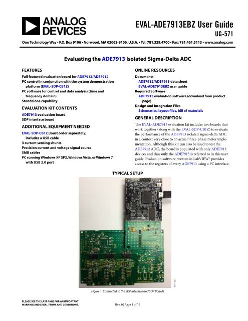
GENERAL DESCRIPTION<br />
The EVAL-ADE7913 evaluation kit includes two boards that<br />
work together (along with the EVAL-SDP-CB1Z) to evaluate<br />
the performance of the ADE7913 isolated sigma-delta ADC<br />
in a context very close to an actual three-phase meter implementation.<br />
Although this kit can also be used to test the<br />
ADE7912 ADC, the board is populated with only ADE7913<br />
devices and thus only the ADE7913 is referred to in this user<br />
guide. Evaluation software, written in LabVIEW® provides<br />
access to the registers of every ADE7913 using a PC interface.<br />
TYPICAL SETUP<br />
11671-002<br />
Figure 1. Connected to the SDP Interface and SDP Boards<br />
PLEASE SEE THE LAST PAGE FOR AN IMPORTANT<br />
WARNING AND LEGAL TERMS AND CONDITIONS. Rev. 0 | Page 1 of 16
<strong>UG</strong>-<strong>571</strong><br />
TABLE OF CONTENTS<br />
Features .............................................................................................. 1<br />
Evaluation Kit Contents ................................................................... 1<br />
Additional Equipment Needed ....................................................... 1<br />
Online Resources .............................................................................. 1<br />
General Description ......................................................................... 1<br />
Typical Setup ..................................................................................... 1<br />
Revision History ............................................................................... 2<br />
Evaluation Board Hardware ............................................................ 3<br />
Overview ........................................................................................ 3<br />
Powering Up the Evaluation Kit Boards .................................... 5<br />
<strong>Analog</strong> Inputs ................................................................................ 5<br />
Setting Up the Evaluation Board as an Energy Meter ............. 7<br />
Evaluation Board Software .............................................................. 8<br />
EVAL-ADE7913EBZ User Guide<br />
Important Disclaimer ...................................................................8<br />
Installing the Drivers ....................................................................8<br />
Installing and Uninstalling the ADE7913 Software .................8<br />
Front Panel .....................................................................................8<br />
Evaluation Software Functions ..................................................... 10<br />
Start the ADE7913 ..................................................................... 10<br />
Waveform Sampling ................................................................... 11<br />
Synchronization Window .......................................................... 12<br />
Emissions Management ............................................................. 12<br />
Temperature Measurement ....................................................... 13<br />
Read and Write Registers .......................................................... 13<br />
Reset the ADE7913 .................................................................... 14<br />
REVISION HISTORY<br />
11/13—Revision 0: Initial Version<br />
Rev. 0 | Page 2 of 16
EVAL-ADE7913EBZ User Guide<br />
EVALUATION BOARD HARDWARE<br />
OVERVIEW<br />
To evaluate the ADE7913, three boards are connected together<br />
(see Figure 1). The ADE7913 evaluation board, which is<br />
populated with three ADE7913 ADCs, can be used as an<br />
implementation example of a three-phase energy meter (see<br />
Figure 2).<br />
The SDP interface board is also provided in the evaluation kit.<br />
The 20-pin connector (P6) of the SDP interface board is<br />
connected to connector P5 of the ADE7913 evaluation board.<br />
The SDP interface board is connected to the SDP Blackfin<br />
<strong>UG</strong>-<strong>571</strong><br />
board (also referred to as SDP-B or EVAL-SDP-CB1Z) using<br />
the 120-pin connector. Be sure to order EVAL-SDP-CB1Z when<br />
ordering your evaluation board kit; the kit and the SDP-B board<br />
are purchased and packaged separately, but must be used<br />
together.<br />
The SDP Blackfin board consists of an ADSP-BF527 microcontroller<br />
that handles all the communications from the PC<br />
to the ADE7913 devices populating the evaluation board (see<br />
Figure 3).<br />
11671-001<br />
Figure 2. ADE7913 Evaluation Board<br />
Rev. 0 | Page 3 of 16
<strong>UG</strong>-<strong>571</strong><br />
EVAL-ADE7913EBZ User Guide<br />
USB<br />
CONN<br />
SDP BLACKFIN BOARD<br />
P8<br />
ADE7913 EVALUATION BOARD<br />
SDP INTERFACE BOARD<br />
NOT POPULATED<br />
MCU AND LCD CIRCUITRY<br />
P6<br />
V1PIN A<br />
TP14<br />
V2PIN A<br />
TP15<br />
PHASE A<br />
ADE7913<br />
FILTER<br />
NETWORK<br />
V1PIN B<br />
TP9<br />
V2PIN B<br />
TP10<br />
PHASE B<br />
ADE7913<br />
FILTER<br />
NETWORK<br />
V1PIN C<br />
TP4<br />
V2PIN C<br />
TP5<br />
PHASE C<br />
ADE7913<br />
FILTER<br />
NETWORK<br />
AGND_<br />
ADC1 A<br />
IMIN A<br />
NOT POPULATED<br />
CF AND RS-485 CIRCUITRY<br />
IPIN A<br />
AGND_<br />
ADC1 B<br />
IMIN B<br />
IPIN B<br />
AGND_<br />
ADC1 C<br />
IMIN C<br />
IPIN C<br />
TP11<br />
TP12<br />
TP13<br />
TP6<br />
TP7<br />
TP8<br />
TP1<br />
TP2<br />
TP3<br />
11671-003<br />
Figure 3. Evaluation Kit Connection Diagram<br />
Rev. 0 | Page 4 of 16
EVAL-ADE7913EBZ User Guide<br />
<strong>UG</strong>-<strong>571</strong><br />
POWERING UP THE EVALUATION KIT BOARDS<br />
The interface board receives power via the USB cable that is<br />
connected to the PC. A 3.3 V regulator then powers the SDP<br />
board microcontroller and the ADE7913 ADCs populating the<br />
evaluation board. No additional power source is required for<br />
the ADE7913 evaluation kit boards.<br />
ANALOG INPUTS<br />
Current and voltage signals are connected at the test pins placed<br />
on the evaluation board. All analog input signals are filtered<br />
using the on-board antialiasing filters before the signals are<br />
connected to the ADE7913 ADCs. The components used on the<br />
board are the values recommended for use with the ADE7913.<br />
Current Sense Inputs (TP3 and TP2, TP8 and TP7, TP13<br />
and TP12 Test Pins)<br />
Every ADE7913 measures the voltage across a shunt at its IP<br />
and IM pins. Figure 4 shows the structure used for the Phase A<br />
current.<br />
The R8, R9, R20, and R21 are 0 Ω resistors that do not need<br />
to be implemented on a real meter board. The R15/C12 and<br />
R16/C15 RC networks are the antialiasing filters. The default<br />
corner frequency of these low-pass filters is 4.8 kHz (1 kΩ/<br />
33 nF). These filters can easily be adjusted by replacing the<br />
components on the evaluation board.<br />
The E1, E2, and E3 ferrite beads filter the high frequency noise<br />
that may be induced into the wires.<br />
The absolute maximum voltage on the IP and IM pins of the<br />
ADE7913 is ±2 V. The D3 and D6 diodes protect the IP and IM<br />
pins against voltages greater than ±1 V. The maximum signal level<br />
permissible at the IP pin of the ADE7913 is ±0.03125 V peak.<br />
The signal range should not exceed ±0.03125 V, with respect to<br />
AGND_ADC, for specified operation.<br />
The Phase A shunt is connected between the TP13 and TP12<br />
test pins.<br />
The other current channels (that is, Phase B and Phase C) have<br />
an identical input structure. The Phase B shunt is connected<br />
between the TP8 and TP7 test pins and the Phase C shunt is<br />
connected between TP3 and TP2.<br />
The shunt maximum value is a function of the maximum<br />
current to be measured on every phase:<br />
where:<br />
31.25×<br />
10<br />
R =<br />
2<br />
31.25×<br />
10<br />
2<br />
−3<br />
−3<br />
×<br />
1<br />
I FS<br />
is the rms value of the full-scale voltage accepted at the ADC<br />
input.<br />
IFS is the maximum current to be measured. It is called the fullscale<br />
current.<br />
Figure 5 shows how a shunt is connected to the Phase A<br />
current input structure. The shunt is connected between P1<br />
and P1’ energy meter Phase A line inputs. TP13 and TP12 test<br />
pins are connected to the shunt measurement poles, while<br />
TP11, the tests pin that is the ground of the Phase A ADE7913<br />
side, is connected to the ground pole of the shunt.<br />
TP13<br />
IPIN<br />
TP11<br />
AGND_ADC1<br />
TO P1'<br />
METER<br />
INPUT<br />
TO P1<br />
METER<br />
INPUT<br />
TP12<br />
IMIN<br />
E1<br />
E2<br />
E3<br />
R8<br />
0Ω<br />
R15<br />
1kΩ<br />
AGND_ADC<br />
R9<br />
0Ω<br />
R16<br />
1kΩ<br />
R20<br />
0kΩ<br />
R21<br />
0kΩ<br />
Figure 4. Phase A Current Input Structure on the Evaluation Board<br />
TP13<br />
IPIN<br />
TP11<br />
AGND_ADC1<br />
TP12<br />
IMIN<br />
E1<br />
E2<br />
E3<br />
C12<br />
33nF<br />
C15<br />
33nF<br />
R8<br />
0Ω<br />
D3<br />
AGND_ADC<br />
R9<br />
0Ω<br />
R15<br />
1kΩ<br />
R16<br />
1kΩ<br />
D6<br />
C12<br />
33nF<br />
C15<br />
33nF<br />
Figure 5. Example of a Shunt Connection<br />
ADE7913<br />
IP<br />
D3<br />
IM<br />
R20<br />
0kΩ<br />
D6<br />
R21<br />
0kΩ<br />
11671-004<br />
ADE7913<br />
IP<br />
IM<br />
11671-005<br />
Rev. 0 | Page 5 of 16
<strong>UG</strong>-<strong>571</strong><br />
Phase Voltage Sense Inputs (TP4, TP9, and TP14<br />
Tests Pins)<br />
The phase-to-neutral voltage input connections on the<br />
ADE7913 evaluation board can be directly connected to the line<br />
voltage sources between TP14 and TP11 for Phase A-to-neutral<br />
voltage, between TP9 and TP6 for Phase B-to-neutral voltage,<br />
and between TP4 and TP1 for Phase C-to-neutral voltage.<br />
These voltages are attenuated using a simple resistor divider<br />
network before they are supplied to the ADE7913. The attenuation<br />
network on the voltage channels is designed so that the<br />
corner frequency (3 dB frequency) of the network matches that<br />
of the antialiasing filters in the current channel inputs. This<br />
prevents the occurrence of large energy errors at low power<br />
factors.<br />
The V1PIN path in Figure 6 shows a typical connection of the<br />
Phase A voltage inputs; the resistor divider consists of three<br />
330 kΩ resistors (R1, R5, and R10) and one 1 kΩ resistor (R14).<br />
The antialiasing filter R14/C11 matches the R12/C9 filter in the<br />
VM path. The absolute maximum voltages on the V1P and VM<br />
pins of the ADE7913 are ±2 V. The D1, D7 and D4, D9 diodes<br />
protect the V1P and VM pins against voltages greater than ±2 V.<br />
The maximum signal level permissible at the V1P pin of the<br />
ADE7913 is ±0.5 V peak. The signal range should not exceed<br />
±0.5 V with respect to AGND_ADC for specified operation.<br />
The E4 ferrite bead filters the high frequency noise that may<br />
be induced into the wires.<br />
Auxiliary Voltage Sense Inputs (TP5, TP10, and TP15<br />
Test Pins)<br />
The auxiliary voltage input connections on the ADE7913<br />
evaluation board can be directly connected to the line voltage<br />
sources between TP15 and TP11 for Phase A auxiliary voltage,<br />
between TP10 and TP6 for Phase B auxiliary voltage, and<br />
between TP5 and TP1 for Phase C auxiliary voltage.<br />
The V2PIN path in Figure 6 shows a typical connection of the<br />
Phase A auxiliary voltage input. It is very similar to the V1PIN<br />
path explained in Phase Voltage Sense Inputs (TP4, TP9, and<br />
TP14 Tests Pins) section.<br />
TP14<br />
V1PIN<br />
TP15<br />
V2PIN<br />
E4<br />
AGND_ADC<br />
E5<br />
R1<br />
330kΩ<br />
R2<br />
330kΩ<br />
EVAL-ADE7913EBZ User Guide<br />
R5<br />
330kΩ<br />
R12<br />
1kΩ<br />
R6<br />
330kΩ<br />
R10<br />
330kΩ<br />
C9<br />
33nF<br />
R14<br />
1kΩ<br />
R11<br />
330kΩ<br />
R13<br />
1kΩ<br />
C11<br />
33nF<br />
AGND_ADC<br />
C10<br />
33nF<br />
AGND_ADC<br />
Figure 6. Phase A Voltage Input Structure on the Evaluation Board<br />
Isolated Ground Pins Management<br />
The ADE7913 package has two isolated ground GNDISO pins:<br />
Pin 2 and Pin 10. Figure 7 presents their management in the<br />
case of a Phase A ADE7913. Internally, Pin 2 is connected to<br />
Pin 10. The decoupling capacitors C3 and C4 on the VDDISO<br />
pin are connected to the closest isolated ground pin, Pin 2. The<br />
decoupling capacitors, C5 and C6 on the analog LDO pin and<br />
C13 and C14 on the voltage reference pin, must be separate<br />
from the VDDISO circuitry and are connected to the isolated<br />
ground Pin 10.<br />
TP11<br />
AGND_ADC1<br />
E2<br />
AGND_ADC<br />
C3<br />
C5<br />
LDO<br />
8<br />
C6 VREF<br />
9<br />
C13 C14<br />
Figure 7. Isolated Ground Pins Management<br />
ADE7913<br />
V1P<br />
The P1 meter input constitutes the AGND_ADC1 signal (see<br />
also Figure 5). ADC_GND1 is then connected to GNDISO pin<br />
(AGND_ADC signal) through a ferrite bead (E2).<br />
C4<br />
VDD ISO<br />
1<br />
2<br />
GND ISO<br />
10<br />
GND ISO<br />
D1<br />
D7<br />
D8<br />
D2<br />
D4<br />
D9<br />
VM<br />
D10<br />
D5<br />
V2P<br />
PHASE A<br />
ADE7913<br />
11671-006<br />
GROUND CONNECTION<br />
BETWEEN PIN 2 AND PIN 10<br />
INTERNAL TO ADE7913<br />
11671-007<br />
Rev. 0 | Page 6 of 16
EVAL-ADE7913EBZ User Guide<br />
<strong>UG</strong>-<strong>571</strong><br />
SETTING UP THE EVALUATION BOARD<br />
AS AN ENERGY METER<br />
Figure 8 shows a typical setup for the ADE7913 evaluation<br />
board. In this example, an energy meter for a 3-phase, 4-wire<br />
wye distribution system is shown. Shunts are used to sense the<br />
phase currents and are connected as shown in Figure 8. The<br />
line voltages are connected directly to the board as shown. The<br />
board is supplied from one power supply provided by the PC<br />
through the USB cable.<br />
PHASE C<br />
PHASE B<br />
PHASE A<br />
Figure 9 shows a setup for the ADE7913 evaluation board as<br />
an energy meter for a 3-phase, 3-wire, delta distribution system.<br />
The Phase B voltage is considered as reference and the V1PIN<br />
test pins of Phase A and Phase C ADE7913 ADCs are connected<br />
to it.<br />
PHASE C<br />
PHASE B<br />
TP11<br />
TP12<br />
TP13<br />
TP14<br />
TP1<br />
TP2<br />
TP3<br />
TP4<br />
AGND_ADC1 A<br />
IMIN A<br />
IPIN A<br />
V1PIN A<br />
AGND_ADC1 C<br />
IMIN C<br />
IPIN C<br />
V1PIN C<br />
PHASE A<br />
ADE7913<br />
PHASE C<br />
ADE7913<br />
NEUTRAL<br />
PHASE A<br />
TP11<br />
TP12<br />
TP13<br />
AGND_ADC1 A<br />
IMIN A<br />
IPIN A<br />
PHASE A<br />
ADE7913<br />
LOAD<br />
Figure 9. Typical Setup for the ADE7913 Evaluation Board<br />
for 3-Phase, 3-Wire Delta Distribution Systems<br />
11671-009<br />
TP14<br />
TP6<br />
TP7<br />
TP8<br />
TP9<br />
V1PIN A<br />
AGND_ADC1 B<br />
IMIN B<br />
IPIN B<br />
V1PIN B<br />
PHASE B<br />
ADE7913<br />
Using the Evaluation Board with Another Microcontroller<br />
It is possible to manage the ADE7913 evaluation board with<br />
a different microcontroller mounted on another board. The<br />
evaluation board can be connected to this second board<br />
through the P5 connector. The SDP interface and the SDP<br />
Blackfin boards are, in this case, unused.<br />
TP1<br />
TP2<br />
TP3<br />
AGND_ADC1 C<br />
IMIN C<br />
IPIN C<br />
PHASE C<br />
ADE7913<br />
TP4<br />
V1PIN C<br />
LOAD<br />
Figure 8. Typical Setup for the ADE7913 Evaluation Board<br />
for 3-Phase, 4-Wire, Wye Distribution System<br />
11671-008<br />
Rev. 0 | Page 7 of 16
<strong>UG</strong>-<strong>571</strong><br />
EVALUATION BOARD SOFTWARE<br />
The ADE7913 evaluation board is supported by Windows®<br />
based software that allows the user to access all the functionality<br />
of the ADE7913.<br />
The software communicates with the microcontroller placed<br />
on the interface board using the USB port. The software<br />
communicates with the SDP Blackfin board using the USB. The<br />
microcontroller communicates with the ADE7913 ADCs placed<br />
on the evaluation board to process the requests that are sent<br />
from the PC.<br />
IMPORTANT DISCLAIMER<br />
The evaluation board contains three ADE7913 ADCs, labeled<br />
Phase A ADE7913, Phase B ADE7913, and Phase C ADE7913.<br />
The software can work with boards containing up to four<br />
ADE7913 ADCs. For this reason, it contains settings referring<br />
to Phase N ADE7913, the eventual fourth ADE7913 (such as<br />
shown in Figure 16, for example). It is safe to disregard any<br />
warnings that may be generated stating that the Phase N<br />
ADE7913 is not populated on board.<br />
INSTALLING THE DRIVERS<br />
When using the ADE7913 evaluation tools for the first time,<br />
a driver must be installed to allow successful communication.<br />
The driver SDPDriversNET.exe can be found in the evaluation<br />
software package in the SDP drivers folder.<br />
To install the driver, follow this procedure:<br />
1. When the Setup Wizard appears, click Next, and follow the<br />
installation instructions.<br />
Figure 10. SDP Drivers Setup<br />
11671-010<br />
EVAL-ADE7913EBZ User Guide<br />
2. When installation is complete, click Finish to close the<br />
window.<br />
Connect the USB cable from the PC to the Blackfin SDP board.<br />
Windows detects the device and locates the correct driver<br />
automatically.<br />
INSTALLING AND UNINSTALLING THE ADE7913<br />
SOFTWARE<br />
The ADE7913 software is supplied with the evaluation software<br />
package. It contains the LabVIEW-based program that runs on<br />
the PC. This program must be installed.<br />
Before using LabView 2010 on the PC for the first time, run an<br />
installer prior to executing the LabVIEW-based program. This<br />
installer is available in the installation_files folder. If a copy of<br />
LabView 2010 is available on the PC, the executable is provided<br />
in the executable folder. The LabView source files are provided<br />
in the LabView_project\source folder.<br />
1. To install the ADE7913 software, double-click<br />
installation_files\setup.exe. This launches the setup<br />
program that automatically installs all the software<br />
components, including the uninstall program, and<br />
creates the required directories.<br />
2. To launch the software, go to the Start/Programs/<br />
ADE7913 Eval Software menu and click ADE7913<br />
Eval Software.<br />
Both the ADE7913 evaluation software program and the NI<br />
run-time engine are easily uninstalled by using the Add/<br />
Remove Programs option in the control panel.<br />
1. Before installing a new version of the ADE7913 evaluation<br />
software, first uninstall the previous version.<br />
2. Select the Add/Remove Programs option in the Windows<br />
control panel.<br />
3. Select the program to uninstall and click the Add/Remove<br />
button.<br />
FRONT PANEL<br />
When the software is launched, the Front Panel is opened. This<br />
panel contains two areas: the main menu on the left, and a box<br />
that displays the name of the communication port used by the<br />
PC to connect to the interface port on the right (see Figure 11).<br />
The software automatically detects the SDP Blackfin board. If<br />
the port detection is successful, the SDP label appears in the IO<br />
Board field, as shown in Figure 11.<br />
Rev. 0 | Page 8 of 16
EVAL-ADE7913EBZ User Guide<br />
<strong>UG</strong>-<strong>571</strong><br />
Figure 11. Front Panel of the ADE7913 Software<br />
Troubleshooting the COM Port Detection<br />
If the software does not detect the SDP Blackfin board, the<br />
message shown in Figure 12 is displayed.<br />
11671-011<br />
Figure 12. SDP Blackfin Board Not Detected Message<br />
If this message appears, the following steps should be taken:<br />
1. Click OK to terminate the program (see Figure 11).<br />
2. Verify that the SDP Blackfin board is connected to the PC<br />
using the USB cable.<br />
3. Ensure that the required drivers are installed as described<br />
in the Installing the Drivers section.<br />
4. Using the Device Manager tool, ensure that the SDP<br />
Blackfin board was recognized by the PC and appears<br />
under the ADI Development Tools entry as <strong>Analog</strong><br />
<strong>Devices</strong> System Demonstration Platform SDP-B.<br />
5. Launch the ADE7913 evaluation software once more.<br />
11671-012<br />
Rev. 0 | Page 9 of 16
<strong>UG</strong>-<strong>571</strong><br />
EVALUATION SOFTWARE FUNCTIONS<br />
The ADE7913 evaluation software allows access to all registers<br />
and features of the ADE7913. The menu options available are<br />
• Start the ADE7913s<br />
• Waveform Sampling<br />
• Synchronization<br />
• Emissions Management<br />
• Temperature Measurement<br />
• Read and Write Registers<br />
• Reset the ADE7913s<br />
• EXIT (stops LabView)<br />
The options provide access to all internal registers and allow<br />
the evaluation of the ADC performance. To access these<br />
functions, click the desired option in the MENU (see Figure 11).<br />
Clicking an option in the MENU displays a window where the<br />
specific function can be accessed. Each window includes an<br />
EXIT button used to return to the main window.<br />
Note that only one option from the MENU can be open at a<br />
time; click EXIT to return to the main window before choosing<br />
another option from the MENU.<br />
START THE ADE7913<br />
The Start the ADE7913s window is shown in Figure 13. The<br />
Phase A ADE7913 is clocked from a 4.096 MHz crystal. It<br />
then generates clock output to the other Phase B and Phase C<br />
ADE7913 ADCs at its CLKOUT pin. The software automatically<br />
sets the Phase A ADE7913 to generate clock output<br />
and start all three ADE7913 ADCs with the following default<br />
settings:<br />
• ADC output frequency set at 8 kHz. Note that in order<br />
to ensure complete coherency of the waveform samples<br />
coming out from all three ADCs, this output frequency<br />
should be the same on all ADCs.<br />
• The bandwidth of the digital low-pass filter of the ADC<br />
is set at 3.3 kHz.<br />
• The third ADC measures the auxiliary voltage instead of<br />
the temperature sensor.<br />
• The Phase C ADE7913 generates a DREADY signal at<br />
its CLKOUT/DREADY pin. This signal is used by the<br />
microcontroller as an external interrupt to start the<br />
acquisition of coherent waveform samples from all<br />
ADE7913 ADCs populating the evaluation board.<br />
If different settings are desired, select them from the boxes in<br />
the upper half of the window. Then, click START PHASE A<br />
ADE7913 FIRST to update the Phase A ADE7913.<br />
EVAL-ADE7913EBZ User Guide<br />
Note that the Phase A ADE7913 clocks the other ADE7913<br />
ADCs populating the evaluation board by enabling CLKOUT<br />
functionality at the CLKOUT/DREADY pin (Bit 0, CLKOUT_EN,<br />
in the CONFIG register set to 1). Always enable CLKOUT if<br />
functional Phase B and Phase C ADE7913 ADCs are required<br />
for evaluation.<br />
Figure 13. Start the ADE7913s<br />
After the Phase A ADE7913 is started correctly, click START<br />
THE OTHER ADE7913s to configure the other ADE7913<br />
ADCs on the evaluation board.<br />
SYNCHRONIZE ALL ADE7913s executes a broadcast write<br />
to the SYNC_SNAP register equal to 0x01 to synchronize all<br />
ADE7913 ADCs of the evaluation board.<br />
ENABLE/DISABLE REGISTERS PROTECTION ON ALL<br />
ADE7913s manages the registers protection of the ADE7913<br />
ADCs. If at least one ADE7913 has the registers protected,<br />
then pressing this option disables the protection by executing<br />
a broadcast write to the Lock register equal to 0x9C. If all<br />
ADE7913 ADCs have the registers unprotected, then pressing<br />
this option enables the protection by executing a broadcast<br />
write to Lock register equal to 0xCA. Note that when the<br />
registers are protected, no register can be further written until<br />
the protection is disabled. It is therefore recommended to<br />
evaluate the ADE7913 ADCs while maintaining the registers<br />
protection disabled.<br />
The bottom half of the window is composed by stacked<br />
windows, each showing the configuration settings of each<br />
ADE7913.<br />
11671-013<br />
Rev. 0 | Page 10 of 16
EVAL-ADE7913EBZ User Guide<br />
<strong>UG</strong>-<strong>571</strong><br />
WAVEFORM SAMPLING<br />
The Waveform Sampling window is shown in Figure 14. It<br />
provides full access to the ADC outputs (waveforms) of the<br />
ADE7913 ADCs that populate the board.<br />
1. Enter an acquisition time (ACCUMULATION TIME)<br />
expressed in milliseconds.<br />
2. Select the ADE7913 ADCs to be analyzed by checking the<br />
A, B, and C boxes. Leave the N box unchecked because the<br />
ADE7913 evaluation board contains only three ADE7913<br />
ADCs.<br />
3. Select START ANALYSIS.<br />
The SDP Blackfin board acquires the waveform samples using<br />
the Phase C ADE7913 DREADY signal as an interrupt. The<br />
green bar under the plot shows the acquisition progress. A box<br />
under the START ANALYSIS button selects which waveform is<br />
visualized in the plot. By default, all the waveforms acquired<br />
from all ADE7913 ADCs selected for analysis are displayed.<br />
• For single waveform visualization, select the desired<br />
waveform under SELECT WAVEFORMS.<br />
• For multiple waveform visualization, select the desired<br />
waveforms under SELECT WAVEFORMS while pressing<br />
the CTRL key.<br />
To write the waveforms into files,<br />
1. Select the folder for file storage (SELECT FOLDER).<br />
2. Select WRITE WAVEFORMS TO FILES.<br />
The program stores every waveform into a file called<br />
Waveform_sample_X.dat, where X is a number between 0<br />
or 8. The order of the waveforms listed in the SELECT<br />
WAVEFORMS box is reflected in the file name identification<br />
number. As the default selects all waveforms to be acquired,<br />
Waveform_sample_0.dat contains Phase A current waveform,<br />
Waveform_sample_1.dat contains Phase A voltage 1 waveform,<br />
Waveform_sample_2.dat contains Phase A voltage 2 waveform,<br />
and so on.<br />
The plot always visualizes 100 ms worth of waveform samples.<br />
If the acquisition time is greater, a scroll bar below the plot<br />
allows the visualization of an additional 100 ms periods.<br />
A Fourier analysis of the acquired waveforms may be enabled<br />
by changing the position of the SELECT ANALYSIS switch.<br />
In this case, the window shown in Figure 15 is enabled. Only<br />
one waveform at a time is visualized in the plot.<br />
The type of windowing may be selected: Hanning, Blackman-<br />
Harris, or none.<br />
Various FFT Settings may be selected: 0 dB level reference may<br />
be at the signal peak, the theoretical maximum, or at a manual<br />
entry. When selecting Signal Peak, the plot uses the amplitude<br />
of the maximum peak of the waveform as the 0 dB level and<br />
writes it in the Manual entry box.<br />
Other selection include the Bandwidth under analysis (default<br />
is between 10 Hz and 4000 Hz), the Fundamental Frequency<br />
Rev. 0 | Page 11 of 16<br />
(the default is 50 Hz), the width of the FFT bins, Fund/Harm<br />
Sideband Bins, (the default is 10 Hz), and the Number of<br />
Harmonics used in the ADC specifications visualized under<br />
the plot (default is 6).<br />
When the FFT plot is visualized, the program calculates and<br />
visualizes the following ADC specifications:<br />
• SNR (signal-to-noise ratio)<br />
• THD (total harmonic distortion)<br />
• SNDR (signal-to-noise and distortion ratio)<br />
• SFDR (spurious-free dynamic range)<br />
• Signal (rms of the fundamental component)<br />
• Noise (rms of the noise)<br />
• Harmonics (rms value of all harmonics)<br />
Figure 14. Waveform Sampling<br />
Figure 15. Fourier Analysis<br />
11671-014<br />
11671-015
<strong>UG</strong>-<strong>571</strong><br />
SYNCHRONIZATION WINDOW<br />
The Synchronization window is shown in Figure 16. It manages<br />
the synchronization process of all ADE7913 ADCs populating<br />
the board.<br />
SYNCHRONIZE ALL ADE7913s executes a broadcast write<br />
to the SYNC_SNAP register equal to 0x01 to synchronize all<br />
ADE7913 ADCs of the evaluation board.<br />
Another second synchronization method uses the internal<br />
counters of every ADE7913 to synchronize them. When<br />
pressed, LATCH AND READ ADE7913s INTERNAL<br />
COUNTERS broadcasts a write to the SYNC_SNAP register<br />
equal to 0x02, latching the counters and then visualizing them<br />
into the CNT_SNAPSHOT boxes. The software then uses the<br />
counter of the ADE7913 used to generate DREADYinterrupts<br />
as a reference to calculate corrections values for each counter.<br />
SYNCHRONIZE ALL ADE7913s BY WRITING ADE7913s<br />
INTERNAL COUNTERS then writes new values into the<br />
internal counters of each ADE7913, synchronizing all<br />
ADE7913 ADCs.<br />
LATCH AND READ ADE7913s INTERNAL COUNTERS<br />
can then be used to read again the internal counters to verify<br />
the achieved synchronization degree.<br />
EVAL-ADE7913EBZ User Guide<br />
EMISSIONS MANAGEMENT<br />
The Emissions Management window is shown in Figure 17. It<br />
manages the EMI_CTRL register that controls the isolated dcto-dc<br />
converter integrated in the ADE7913 ADCs.<br />
Figure 17. Emissions Management<br />
The window displays a picture showing the relation between<br />
the bits of the EMI_CTRL register, the 1.024 MHz clock, and<br />
the PWM control pulses. In the middle section of the window,<br />
the program can read and write the EMI_CTRL registers of all<br />
ADE7913 ADCs populating the evaluation board.<br />
Initialize the Phase A ADE79133 EMI_CTRL register as follows<br />
for best emissions performance:<br />
• EMI_CTRLA to 0x55<br />
• EMI_CTRLB to 0xAA<br />
• EMI_CTRLC to 0x55<br />
• EMI_CTRLN to 0xAA<br />
11671-017<br />
Figure 16. ADE7913s Synchronization<br />
11671-016<br />
Rev. 0 | Page 12 of 16
EVAL-ADE7913EBZ User Guide<br />
TEMPERATURE MEASUREMENT<br />
The Temperature Measurement window is shown in Figure 18.<br />
The left half of the window selects the temperature sensor<br />
measurement on each ADE7913. The Temperature Offset<br />
boxes display the content of the TEMPOS register of each<br />
ADE7913.<br />
After selecting the temperature sensor, press WRITE CONFIG<br />
REGISTERS to write the new selection into the CONFIG<br />
registers. READ CONFIG REGISTERS reads the CONFIG<br />
registers and visualizes the state of Bit 3 (TEMP_EN) into the<br />
temperature sensor selection switch and the CONFIG register<br />
value into the boxes at the bottom of the window.<br />
READ V2WV REGISTER reads the V2WV registers of each<br />
ADE7913 and displays its content into the V2/Temperature<br />
reading boxes. The software computes the temperature in °C<br />
and displays it in the Temperature [deg C] boxes on the right<br />
side of the window.<br />
The Temperature Gain Correction (FP) and the Temperature<br />
Offset Correction factors are introduced in floating point<br />
format into the boxes placed on the lower left side of the<br />
window. They are used by the software to compute the<br />
temperature of each ADE7913.<br />
<strong>UG</strong>-<strong>571</strong><br />
READ AND WRITE REGISTERS<br />
The Read and Write Registers window is shown in Figure 19.<br />
Every register of each ADE7913 populating the board can be<br />
accessed using the boxes beneath Identify which ADE7913<br />
to access and then clicking WRITE or READ.<br />
The registers can be accessed by name or address using the<br />
Register Identification Criteria switch.<br />
Figure 19. Read and Write Registers<br />
11671-018<br />
11671-019<br />
Figure 18. Temperature Measurement<br />
Rev. 0 | Page 13 of 16
<strong>UG</strong>-<strong>571</strong><br />
EVAL-ADE7913EBZ User Guide<br />
RESET THE ADE7913<br />
The Reset the ADE7913s window is shown in Figure 20.<br />
Use SELECT ADE7913 TO RESET to select which ADE7913<br />
to reset. An individual ADE7913 or all ADE7913 ADCs may be<br />
selected. RESET then resets the selected ADE7913 by writing<br />
10 bytes with a value of 0x00 at Address 0x00.<br />
11671-020<br />
Figure 20. Reset the ADE7913s<br />
Rev. 0 | Page 14 of 16
EVAL-ADE7913EBZ User Guide<br />
<strong>UG</strong>-<strong>571</strong><br />
NOTES<br />
Rev. 0 | Page 15 of 16
<strong>UG</strong>-<strong>571</strong><br />
EVAL-ADE7913EBZ User Guide<br />
NOTES<br />
ESD Caution<br />
ESD (electrostatic discharge) sensitive device. Charged devices and circuit boards can discharge without detection. Although this product features patented or proprietary protection<br />
circuitry, damage may occur on devices subjected to high energy ESD. Therefore, proper ESD precautions should be taken to avoid performance degradation or loss of functionality.<br />
Legal Terms and Conditions<br />
By using the evaluation board discussed herein (together with any tools, components documentation or support materials, the “Evaluation Board”), you are agreeing to be bound by the terms and conditions<br />
set forth below (“Agreement”) unless you have purchased the Evaluation Board, in which case the <strong>Analog</strong> <strong>Devices</strong> Standard Terms and Conditions of Sale shall govern. Do not use the Evaluation Board until you<br />
have read and agreed to the Agreement. Your use of the Evaluation Board shall signify your acceptance of the Agreement. This Agreement is made by and between you (“Customer”) and <strong>Analog</strong> <strong>Devices</strong>, Inc.<br />
(“ADI”), with its principal place of business at One Technology Way, Norwood, MA 02062, USA. Subject to the terms and conditions of the Agreement, ADI hereby grants to Customer a free, limited, personal,<br />
temporary, non-exclusive, non-sublicensable, non-transferable license to use the Evaluation Board FOR EVALUATION PURPOSES ONLY. Customer understands and agrees that the Evaluation Board is provided<br />
for the sole and exclusive purpose referenced above, and agrees not to use the Evaluation Board for any other purpose. Furthermore, the license granted is expressly made subject to the following additional<br />
limitations: Customer shall not (i) rent, lease, display, sell, transfer, assign, sublicense, or distribute the Evaluation Board; and (ii) permit any Third Party to access the Evaluation Board. As used herein, the term<br />
“Third Party” includes any entity other than ADI, Customer, their employees, affiliates and in-house consultants. The Evaluation Board is NOT sold to Customer; all rights not expressly granted herein, including<br />
ownership of the Evaluation Board, are reserved by ADI. CONFIDENTIALITY. This Agreement and the Evaluation Board shall all be considered the confidential and proprietary information of ADI. Customer may<br />
not disclose or transfer any portion of the Evaluation Board to any other party for any reason. Upon discontinuation of use of the Evaluation Board or termination of this Agreement, Customer agrees to<br />
promptly return the Evaluation Board to ADI. ADDITIONAL RESTRICTIONS. Customer may not disassemble, decompile or reverse engineer chips on the Evaluation Board. Customer shall inform ADI of any<br />
occurred damages or any modifications or alterations it makes to the Evaluation Board, including but not limited to soldering or any other activity that affects the material content of the Evaluation Board.<br />
Modifications to the Evaluation Board must comply with applicable law, including but not limited to the RoHS Directive. TERMINATION. ADI may terminate this Agreement at any time upon giving written notice<br />
to Customer. Customer agrees to return to ADI the Evaluation Board at that time. LIMITATION OF LIABILITY. THE EVALUATION BOARD PROVIDED HEREUNDER IS PROVIDED “AS IS” AND ADI MAKES NO<br />
WARRANTIES OR REPRESENTATIONS OF ANY KIND WITH RESPECT TO IT. ADI SPECIFICALLY DISCLAIMS ANY REPRESENTATIONS, ENDORSEMENTS, GUARANTEES, OR WARRANTIES, EXPRESS OR IMPLIED, RELATED<br />
TO THE EVALUATION BOARD INCLUDING, BUT NOT LIMITED TO, THE IMPLIED WARRANTY OF MERCHANTABILITY, TITLE, FITNESS FOR A PARTICULAR PURPOSE OR NONINFRINGEMENT OF INTELLECTUAL<br />
PROPERTY RIGHTS. IN NO EVENT WILL ADI AND ITS LICENSORS BE LIABLE FOR ANY INCIDENTAL, SPECIAL, INDIRECT, OR CONSEQUENTIAL DAMAGES RESULTING FROM CUSTOMER’S POSSESSION OR USE OF<br />
THE EVALUATION BOARD, INCLUDING BUT NOT LIMITED TO LOST PROFITS, DELAY COSTS, LABOR COSTS OR LOSS OF GOODWILL. ADI’S TOTAL LIABILITY FROM ANY AND ALL CAUSES SHALL BE LIMITED TO THE<br />
AMOUNT OF ONE HUNDRED US DOLLARS ($100.00). EXPORT. Customer agrees that it will not directly or indirectly export the Evaluation Board to another country, and that it will comply with all applicable<br />
United States federal laws and regulations relating to exports. GOVERNING LAW. This Agreement shall be governed by and construed in accordance with the substantive laws of the Commonwealth of<br />
Massachusetts (excluding conflict of law rules). Any legal action regarding this Agreement will be heard in the state or federal courts having jurisdiction in Suffolk County, Massachusetts, and Customer hereby<br />
submits to the personal jurisdiction and venue of such courts. The United Nations Convention on Contracts for the International Sale of Goods shall not apply to this Agreement and is expressly disclaimed.<br />
©2013 <strong>Analog</strong> <strong>Devices</strong>, Inc. All rights reserved. Trademarks and<br />
registered trademarks are the property of their respective owners.<br />
<strong>UG</strong>11671-0-11/13(0)<br />
Rev. 0 | Page 16 of 16


