

ADF4251 Dual Fractional-N/Interger-N Frequency ... - Analog Devices
ADF4251 Dual Fractional-N/Interger-N Frequency ... - Analog Devices
ADF4251 Dual Fractional-N/Interger-N Frequency ... - Analog Devices

You also want an ePaper? Increase the reach of your titles
YUMPU automatically turns print PDFs into web optimized ePapers that Google loves.
<strong>Dual</strong> <strong>Fractional</strong>-N/Integer-N<br />
<strong>Frequency</strong> Synthesizer<br />
<strong>ADF4251</strong><br />
FEATURES<br />
3.0 GHz <strong>Fractional</strong>-N/1.2 GHz Integer-N<br />
2.7 V to 3.3 V Power Supply<br />
Separate V P Allows Extended Tuning Voltage to 5 V<br />
Programmable <strong>Dual</strong> Modulus Prescaler<br />
RF: 4/5, 8/9<br />
IF: 8/9, 16/17, 32/33, 64/65<br />
Programmable Charge Pump Currents<br />
3-Wire Serial Interface<br />
Digital Lock Detect<br />
Power-Down Mode<br />
Programmable Modulus on <strong>Fractional</strong>-N Synthesizer<br />
Trade-Off Noise versus Spurious Performance<br />
Software and Hardware Power-Down<br />
APPLICATIONS<br />
Base Stations for Mobile Radio (GSM, PCS, DCS,<br />
CDMA, WCDMA)<br />
Wireless Handsets (GSM, PCS, DCS, CDMA, WCDMA,<br />
PHS)<br />
Wireless LANs<br />
Communications Test Equipment<br />
CATV Equipment<br />
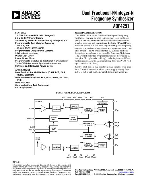
GENERAL DESCRIPTION<br />
The <strong>ADF4251</strong> is a dual fractional-N/integer-N frequency<br />
synthesizer that can be used to implement local oscillators<br />
(LO) in the upconversion and downconversion sections of<br />
wireless receivers and transmitters. Both the RF and IF synthesizers<br />
consist of a low noise digital PFD (phase frequency<br />
detector), a precision charge pump, and a programmable reference<br />
divider. The RF synthesizer has a - based fractional<br />
interpolator that allows programmable fractional-N division.<br />
The IF synthesizer has programmable integer-N counters. A<br />
complete PLL (phase-locked loop) can be implemented if the<br />
synthesizer is used with an external loop filter and VCO (voltage<br />
controlled oscillator).<br />
Control of all the on-chip registers is via a simple 3-wire interface.<br />
The devices operate with a power supply ranging from<br />
2.7 V to 3.3 V and can be powered down when not in use.<br />
FUNCTIONAL BLOCK DIAGRAM<br />
V DD 1 V DD 2 V DD 3 DV DD V P 1 V P 2 R SET<br />
<strong>ADF4251</strong><br />
REFERENCE<br />
4-BIT R<br />
REF<br />
2<br />
IN COUNTER<br />
DOUBLER<br />
PHASE<br />
FREQUENCY<br />
DETECTOR<br />
CHARGE<br />
PUMP<br />
CE<br />
CP RF<br />
MUXOUT<br />
OUTPUT<br />
MUX<br />
LOCK<br />
DETECT<br />
CLK<br />
DATA<br />
LE<br />
FROM<br />
REFIN<br />
24-BIT<br />
DATA<br />
REGISTER<br />
FRACTIONAL N<br />
RF DIVIDER<br />
INTEGER N<br />
IF DIVIDER<br />
RF IN A<br />
RF IN B<br />
IF IN B<br />
IF IN A<br />
2<br />
DOUBLER<br />
15-BIT R<br />
COUNTER<br />
PHASE<br />
FREQUENCY<br />
DETECTOR<br />
CHARGE<br />
PUMP<br />
CP IF<br />
A GND 1 A GND 2 D GND CP GND 1 CP GND 2<br />
REV. 0<br />
Information furnished by <strong>Analog</strong> <strong>Devices</strong> is believed to be accurate and<br />
reliable. However, no responsibility is assumed by <strong>Analog</strong> <strong>Devices</strong> for its<br />
use, nor for any infringements of patents or other rights of third parties that<br />
may result from its use. No license is granted by implication or otherwise<br />
under any patent or patent rights of <strong>Analog</strong> <strong>Devices</strong>. Trademarks and<br />
registered trademarks are the property of their respective owners.<br />
One Technology Way, P.O. Box 9106, Norwood, MA 02062-9106, U.S.A.<br />
Tel: 781/329-4700<br />
www.analog.com<br />
Fax: 781/326-8703 © 2003 <strong>Analog</strong> <strong>Devices</strong>, Inc. All rights reserved.
<strong>ADF4251</strong>–SPECIFICATIONS 1 (V DD 1 = V DD 2 = V DD 3 = DV DD = 3 V 10%, V P 1 = V P 2 = 5 V 10%, GND = 0 V,<br />
R SET = 2.7 k, dBm referred to 50 , T A = T MIN to T MAX , unless otherwise noted.)<br />
Parameter B Version Unit Test Conditions/Comments<br />
RF CHARACTERISTICS<br />
RF Input <strong>Frequency</strong> (RF IN A, RF IN B) 2 0.25/3.0 GHz min/max<br />
RF Input Sensitivity –10/0 dBm min/max<br />
RF Input <strong>Frequency</strong> (RF IN A, RF IN B) 2 0.1/3.0 GHz min/max Input Level = –8/0 dBm min/max<br />
RF Phase Detector <strong>Frequency</strong> 30 MHz max Guaranteed by Design<br />
Allowable Prescaler Output <strong>Frequency</strong> 375 MHz max<br />
IF CHARACTERISTICS<br />
IF Input <strong>Frequency</strong> (IF IN A, IF IN B) 2 50/1200 MHz min/max<br />
IF Input Sensitivity –10/0 dBm min/max<br />
IF Phase Detector <strong>Frequency</strong> 55 MHz max Guaranteed by Design<br />
Allowable Prescaler Output <strong>Frequency</strong> 150 MHz max<br />
REFERENCE CHARACTERISTICS<br />
REF IN Input <strong>Frequency</strong> 250 MHz max For f < 10 MHz, use dc-coupled square<br />
wave (0 to V DD ).<br />
REF IN Input Sensitivity 0.5/V DD 1 V p-p min/max AC-coupled. When dc-coupled, use<br />
0 to V DD max (CMOS compatible).<br />
REF IN Input Current ±100 µA max<br />
REF IN Input Capacitance 10 pF max<br />
CHARGE PUMP<br />
RF I CP Sink/Source High Value 4.375 mA typ See Table V<br />
Low Value 625 µA typ<br />
IF I CP Sink/Source High Value 5 mA typ See Table IX<br />
Low Value 625 µA typ<br />
I CP Three-State Leakage Current 1 nA typ<br />
RF Sink and Source Current Matching 2 % typ 0.5 V < V CP < V P – 0.5<br />
IF Sink and Source Current Matching 2 % typ<br />
I CP vs. V CP 2 % typ 0.5 V < V CP < V P – 0.5<br />
I CP vs. Temperature 2 % typ V CP = V P /2<br />
LOGIC INPUTS<br />
V INH , Input High Voltage 1.35 V min<br />
V INL , Input Low Voltage 0.6 V max<br />
I INH /I INL , Input Current ±1 µA max<br />
C IN Input Capacitance 10 pF max<br />
LOGIC OUTPUTS<br />
V OH , Output High Voltage V DD – 0.4 V min I OH = 0.2 mA<br />
V OL , Output Low Voltage 0.4 V max I OL = 0.2 mA<br />
POWER SUPPLIES<br />
V DD 1 , V DD 2, V DD 3 2.7/3.3 V min/V max<br />
DV DD V DD 1<br />
V P 1, V P 2 V DD 1/5.5 V min/V max<br />
3<br />
I DD RF + IF 13 mA typ 16 mA max<br />
RF Only 10 mA typ 13 mA max<br />
IF Only 4 mA typ 5.5 mA max<br />
Low Power Sleep Mode/Power-Down 10 pA typ<br />
RF NOISE AND SPURIOUS CHARACTERISTICS<br />
Noise Floor –141 dBc/Hz typ @ 20 MHz PFD <strong>Frequency</strong><br />
In-Band Phase Noise Performance 4<br />
@ VCO Output<br />
Lowest Spur Mode –90 dBc/Hz typ RF OUT = 1.8 GHz, PFD = 20 MHz<br />
Low Noise and Spur Mode –95 dBc/Hz typ RF OUT = 1.8 GHz, PFD = 20 MHz<br />
Lowest Noise Mode –103 dBc/Hz typ RF OUT = 1.8 GHz, PFD = 20 MHz<br />
Spurious Signals<br />
See Typical Performance Characteristics<br />
NOTES<br />
1 Operating Temperature Range (B Version): –40°C to +85°C.<br />
2 Use a square wave for frequencies less than F MIN .<br />
3 RF = 1 GHz, RF PFD = 10 MHz, MOD = 4095, IF = 500 MHz, IF PFD = 200 kHz, REF = 10 MHz, V DD = 3 V, V P1 = 5 V, and V P2 = 3 V.<br />
4 The in-band phase noise is measured with the EVAL-<strong>ADF4251</strong>EB2 Evaluation Board and the HP5500E Phase Noise Test System. The spectrum analyzer provides the<br />
REF IN for the synthesizer (f REFOUT = 10 MHz @ 0 dBm). F OUT = 1.74 GHz, F REF = 20 MHz, N = 87, MOD = 100, Channel Spacing = 200 kHz, V DD = 3.3 V, and V P = 5 V.<br />
Specifications subject to change without notice.<br />
–2–<br />
REV. 0
TIMING CHARACTERISTICS *<br />
Limit at<br />
T MIN to T MAX<br />
Parameter (B Version) Unit Test Conditions/Comments<br />
t 1 10 ns min LE Setup Time<br />
t 2 10 ns min DATA to CLOCK Setup Time<br />
t 3 10 ns min DATA to CLOCK Hold Time<br />
t 4 25 ns min CLOCK High Duration<br />
t 5 25 ns min CLOCK Low Duration<br />
t 6 10 ns min CLOCK to LE Setup Time<br />
t 7 20 ns min LE Pulsewidth<br />
*Guaranteed by design but not production tested.<br />
<strong>ADF4251</strong><br />
(V DD 1 = V DD 2 = V DD 3 = DV DD = 3 V 10%, V P 1 = V P 2 = 5 V 10%, GND = 0 V, unless otherwise noted.)<br />
CLOCK<br />
t 2<br />
t 3<br />
t 4 t 5<br />
DATA<br />
DB23<br />
(MSB)<br />
DB22<br />
DB2<br />
DB1<br />
(CONTROL BIT C2)<br />
DB0 (LSB)<br />
(CONTROL BIT C1)<br />
LE<br />
t 1<br />
t 7<br />
t 6<br />
LE<br />
Figure 1. Timing Diagram<br />
REV. 0<br />
–3–
<strong>ADF4251</strong><br />
ABSOLUTE MAXIMUM RATINGS 1, 2<br />
(T A = 25°C, unless otherwise noted.)<br />
V DD 1, V DD 2, V DD 3, DV DD to GND 3 . . . . . . . . –0.3 V to +4 V<br />
REF IN , RF IN A, RF IN B to GND . . . . . . –0.3 V to V DD + 0.3 V<br />
V P 1, V P 2 to GND . . . . . . . . . . . . . . . . . . . . . –0.3 V to +5.8 V<br />
V P 1, V P 2 to V DD 1 . . . . . . . . . . . . . . . . . . . . . –3.3 V to +3.5 V<br />
Digital I/O Voltage to GND . . . . . . . . –0.3 V to V DD + 0.3 V<br />
<strong>Analog</strong> I/O Voltage to GND . . . . . . . . –0.3 V to V DD + 0.3 V<br />
Operating Temperature Range<br />
Industrial (B Version) . . . . . . . . . . . . . . . . –40°C to +85°C<br />
Storage Temperature Range . . . . . . . . . . . . –65°C to +150°C<br />
Maximum Junction Temperature . . . . . . . . . . . . . . . . . 150°C<br />
LFCSP JA Thermal Impedance . . . . . . . . . . . . . . . . 122°C/W<br />
Soldering Reflow Temperature<br />
Vapor Phase (60 sec max) . . . . . . . . . . . . . . . . . . . . . 240°C<br />
IR Reflow (20 sec max) . . . . . . . . . . . . . . . . . . . . . . . 240°C<br />
NOTES<br />
1 Stresses above those listed under Absolute Maximum Ratings may cause permanent<br />
damage to the device. This is a stress rating only and functional operation of<br />
the device at these or any other conditions above those listed in the operational<br />
sections of this specification is not implied. Exposure to absolute maximum rating<br />
conditions for extended periods may affect device reliability.<br />
2 This device is a high performance RF integrated circuit with an ESD rating<br />
of
<strong>ADF4251</strong><br />
PIN FUNCTION DESCRIPTIONS<br />
Mnemonic<br />
CP RF<br />
CP GND 1<br />
RF IN A<br />
RF IN B<br />
A GND 1<br />
MUXOUT<br />
REF IN<br />
CE<br />
D GND<br />
CLK<br />
DATA<br />
LE<br />
R SET<br />
A GND 2<br />
IF IN B<br />
IF IN A<br />
DV DD<br />
CP GND 2<br />
CP IF<br />
V P 2<br />
V DD 2<br />
V DD 3<br />
V DD 1<br />
V P 1<br />
Function<br />
RF Charge Pump Output. This is normally connected to a loop filter that drives the input to an external VCO.<br />
RF Charge Pump Ground<br />
Input to the RF Prescaler. This small signal input is normally taken from the VCO.<br />
Complementary Input to the RF Prescaler<br />
<strong>Analog</strong> Ground for the RF Synthesizer<br />
This multiplexer output allows either the RF or IF lock detect, the scaled RF or IF, or the scaled reference frequency<br />
to be accessed externally.<br />
Reference Input. This is a CMOS input with a nominal threshold of V DD /2 and an equivalent input resistance of<br />
100 kW. This input can be driven from a TTL or CMOS crystal oscillator.<br />
Chip Enable. A Logic Low on this bit powers down the device and puts the charge pump outputs into three-state.<br />
A Logic High on this pin powers up the device, depending on the status of the software power-down bits.<br />
Digital Ground for the <strong>Fractional</strong> Interpolator<br />
Serial Clock Input. This serial clock is used to clock in the serial data to the registers. The data is latched into the<br />
shift register on the CLK rising edge. This input is a high impedance CMOS input.<br />
Serial Data Input. The serial data is loaded MSB first with the three LSBs being the control bits. This input is a<br />
high impedance CMOS input.<br />
Load Enable, CMOS Input. When LE goes high, the data stored in the shift registers is loaded into one of the<br />
seven latches, the latch being selected using the control bits.<br />
Connecting a resistor between this pin and ground sets the minimum charge pump output current. The relationship<br />
between I CP and R SET is:<br />
ICP MIN = 1.<br />
6875<br />
RSET<br />
Therefore, with R SET = 2.7 kW, I CP MIN = 0.625 mA.<br />
Ground for the IF Synthesizer<br />
Complementary Input to the IF Prescaler<br />
Input to the IF Prescaler. This small signal input is normally taken from the IF VCO.<br />
Positive Power Supply for the <strong>Fractional</strong> Interpolator Section. Decoupling capacitors to the ground plane should<br />
be placed as close as possible to this pin. DV DD must have the same voltage as V DD 1, V DD 2, and V DD 3.<br />
IF Charge Pump Ground<br />
IF Charge Pump Output. This is normally connected to a loop filter that drives the input to an external VCO.<br />
IF Charge Pump Power Supply. Decoupling capacitors to the ground plane should be placed as close as possible<br />
to this pin. This voltage should be greater than or equal to V DD 2.<br />
Positive Power Supply for the IF Section. Decoupling capacitors to the ground plane should be placed as close as<br />
possible to this pin. V DD 2 has a value 3 V ± 10%. V DD 2 must have the same voltage as V DD 1, V DD 3, and DV DD .<br />
Positive Power Supply for the RF Digital Section. Decoupling capacitors to the ground plane should be placed as close<br />
as possible to this pin. V DD 3 has a value 3 V ± 10%. V DD 3 must have the same voltage as V DD 1, V DD 2, and DV DD .<br />
Positive Power Supply for the RF <strong>Analog</strong> Section. Decoupling capacitors to the ground plane should be placed as close<br />
as possible to this pin. V DD 1 has a value 3 V ± 10%. V DD 1 must have the same voltage as V DD 2, V DD 3, and DV DD .<br />
RF Charge Pump Power Supply. Decoupling capacitors to the ground plane should be placed as close as possible<br />
to this pin. This voltage should be greater than or equal to V DD 1.<br />
REV. 0<br />
–5–
<strong>ADF4251</strong><br />
V DD 1 V DD 2 V DD 3 DV DD V P 1 V P 2 R SET<br />
<strong>ADF4251</strong><br />
REFERENCE<br />
4-BIT R<br />
REF<br />
2<br />
IN COUNTER<br />
DOUBLER<br />
PHASE<br />
FREQUENCY<br />
DETECTOR<br />
CHARGE<br />
PUMP<br />
CE<br />
CP RF<br />
MUXOUT<br />
OUTPUT<br />
MUX<br />
LOCK<br />
DETECT<br />
CLK<br />
DATA<br />
LE<br />
FROM<br />
REFIN<br />
24-BIT<br />
DATA<br />
REGISTER<br />
FRACTIONAL N<br />
RF DIVIDER<br />
INTEGER N<br />
IF DIVIDER<br />
RF IN A<br />
RF IN B<br />
IF IN B<br />
IF IN A<br />
2<br />
DOUBLER<br />
15-BIT R<br />
COUNTER<br />
PHASE<br />
FREQUENCY<br />
DETECTOR<br />
CHARGE<br />
PUMP<br />
CP IF<br />
A GND 1 A GND 2 D GND CP GND 1 CP GND 2<br />
Figure 2. Detailed Functional Block Diagram<br />
–6–<br />
REV. 0
Typical Performance Characteristics–<strong>ADF4251</strong><br />
OUTPUT POWER – dB<br />
0<br />
–10<br />
–20<br />
–30<br />
–40<br />
–50<br />
–60<br />
–70<br />
V DD = 3V, V P = 5V<br />
I CP = 1.875mA<br />
PFD FREQUENCY = 10MHz<br />
CHANNEL STEP = 200kHz<br />
LOOP BANDWIDTH = 20kHz<br />
FRACTION = 59/100<br />
RBW = 10Hz<br />
REFERENCE<br />
LEVEL = – 4.2dBm<br />
OUTPUT POWER – dB<br />
0<br />
–10<br />
–20<br />
–30<br />
–40<br />
–50<br />
–60<br />
–70<br />
V DD = 3V, V P = 5V<br />
I CP = 1.875mA<br />
PFD FREQUENCY = 10MHz<br />
CHANNEL STEP = 200kHz<br />
LOOP BANDWIDTH = 20kHz<br />
FRACTION = 59/100<br />
RBW = 1kHz<br />
–50dBc@<br />
100kHz<br />
REFERENCE<br />
LEVEL = – 4.2dBm<br />
–80<br />
–99.19dBc/Hz<br />
–80<br />
–90<br />
–90<br />
–100<br />
–2kHz<br />
–1kHz 1.7518GHz 1kHz 2kHz<br />
FREQUENCY<br />
–100<br />
–400kHz –200kHz 1.7518GHz 200kHz 400kHz<br />
FREQUENCY<br />
TPC 1. Phase Noise Plot, Lowest Noise Mode,<br />
1.7518 GHz RF OUT , 10 MHz PFD <strong>Frequency</strong>,<br />
200 kHz Channel Step Resolution<br />
TPC 4. Spurious Plot, Lowest Noise Mode,<br />
1.7518 GHz RF OUT , 10 MHz PFD <strong>Frequency</strong>,<br />
200 kHz Channel Step Resolution<br />
OUTPUT POWER – dB<br />
0<br />
–10<br />
–20<br />
–30<br />
–40<br />
–50<br />
–60<br />
–70<br />
V DD = 3V, V P = 5V<br />
I CP = 1.875mA<br />
PFD FREQUENCY = 10MHz<br />
CHANNEL STEP = 200kHz<br />
LOOP BANDWIDTH = 20kHz<br />
FRACTION = 59/100<br />
RBW = 10Hz<br />
REFERENCE<br />
LEVEL = – 4.2dBm<br />
–90.36dBc/Hz<br />
OUTPUT POWER – dB<br />
0<br />
–10<br />
–20<br />
–30<br />
–40<br />
–50<br />
–60<br />
–70<br />
V DD = 3V, V P = 5V<br />
I CP = 1.875mA<br />
PFD FREQUENCY = 10MHz<br />
CHANNEL STEP = 200kHz<br />
LOOP BANDWIDTH = 20kHz<br />
FRACTION = 59/100<br />
RBW = 1kHz<br />
–51dBc@<br />
100kHz<br />
REFERENCE<br />
LEVEL = – 4.2dBm<br />
–80<br />
–80<br />
–90<br />
–90<br />
–100<br />
–2kHz<br />
–1kHz 1.7518GHz 1kHz 2kHz<br />
FREQUENCY<br />
–100<br />
–400kHz<br />
–200kHz 1.7518GHz 200kHz 400kHz<br />
FREQUENCY<br />
TPC 2. Phase Noise Plot, Low Noise and Spur<br />
Mode, 1.7518 GHz RF OUT , 10 MHz PFD <strong>Frequency</strong>,<br />
200 kHz Channel Step Resolution<br />
TPC 5. Spurious Plot, Low Noise and Spur Mode,<br />
1.7518 GHz RF OUT , 10 MHz PFD <strong>Frequency</strong>,<br />
200 kHz Channel Step Resolution<br />
OUTPUT POWER – dB<br />
0<br />
–10<br />
–20<br />
–30<br />
–40<br />
–50<br />
–60<br />
–70<br />
V DD = 3V, V P = 5V<br />
I CP = 1.875mA<br />
PFD FREQUENCY = 10MHz<br />
CHANNEL STEP = 200kHz<br />
LOOP BANDWIDTH = 20kHz<br />
FRACTION = 59/100<br />
RBW = 10Hz<br />
REFERENCE<br />
LEVEL = – 4.2dBm<br />
–85.86dBc/Hz<br />
OUTPUT POWER – dB<br />
0<br />
–10<br />
–20<br />
–30<br />
–40<br />
–50<br />
–60<br />
–70<br />
V DD = 3V, V P = 5V<br />
I CP = 1.875mA<br />
PFD FREQUENCY = 10MHz<br />
CHANNEL STEP = 200kHz<br />
LOOP BANDWIDTH = 20kHz<br />
FRACTION = 59/100<br />
RBW = 1kHz<br />
–72dBc@<br />
100kHz<br />
REFERENCE<br />
LEVEL = – 4.2dBm<br />
–80<br />
–80<br />
–90<br />
–90<br />
–100<br />
–2kHz<br />
–1kHz 1.7518GHz 1kHz 2kHz<br />
FREQUENCY<br />
–100<br />
–400kHz<br />
–200kHz 1.7518GHz 200kHz 400kHz<br />
FREQUENCY<br />
TPC 3. Phase Noise Plot, Lowest Spur Mode,<br />
1.7518 GHz RF OUT , 10 MHz PFD <strong>Frequency</strong>,<br />
200 kHz Channel Step Resolution<br />
TPC 6. Spurious Plot, Lowest Spur Mode,<br />
1.7518 GHz RF OUT , 10 MHz PFD <strong>Frequency</strong>,<br />
200 kHz Channel Step Resolution<br />
TPCs 1–12 attained using EVAL-ADF4252EB1 Evaluation Board; measurements from HP8562E spectrum analyzer.<br />
REV. 0<br />
–7–
<strong>ADF4251</strong><br />
OUTPUT POWER – dB<br />
0<br />
–10<br />
–20<br />
–30<br />
–40<br />
–50<br />
–60<br />
–70<br />
–80<br />
V DD = 3V, V P = 5V<br />
I CP = 1.875mA<br />
PFD FREQUENCY = 20MHz<br />
CHANNEL STEP = 200kHz<br />
LOOP BANDWIDTH = 20kHz<br />
FRACTION = 59/100<br />
RBW = 10Hz<br />
REFERENCE<br />
LEVEL = – 4.2dBm<br />
–102dBc/Hz<br />
OUTPUT POWER – dB<br />
0<br />
–10<br />
–20<br />
–30<br />
–40<br />
–50<br />
–60<br />
–70<br />
–80<br />
V DD = 3V, V P = 5V<br />
I CP = 1.875mA<br />
PFD FREQUENCY = 20MHz<br />
CHANNEL STEP = 200kHz<br />
LOOP BANDWIDTH = 20kHz<br />
FRACTION = 59/100<br />
RBW = 1kHz<br />
–53dBc@<br />
100kHz<br />
REFERENCE<br />
LEVEL = – 4.2dBm<br />
–90<br />
–90<br />
–100<br />
–2kHz<br />
–1kHz 1.7518GHz 1kHz 2kHz<br />
FREQUENCY<br />
–100<br />
–400kHz –200kHz 1.7518GHz 200kHz 400kHz<br />
FREQUENCY<br />
TPC 7. Phase Noise Plot, Lowest Noise Mode,<br />
1.7518 GHz RF OUT , 20 MHz PFD <strong>Frequency</strong>,<br />
200 kHz Channel Step Resolution<br />
TPC 10. Spurious Plot, Lowest Noise Mode,<br />
1.7518 GHz RF OUT , 20 MHz PFD <strong>Frequency</strong>,<br />
200 kHz Channel Step Resolution<br />
OUTPUT POWER – dB<br />
0<br />
–10<br />
–20<br />
–30<br />
–40<br />
–50<br />
–60<br />
–70<br />
V DD = 3V, V P = 5V<br />
I CP = 1.875mA<br />
PFD FREQUENCY = 20MHz<br />
CHANNEL STEP = 200kHz<br />
LOOP BANDWIDTH = 20kHz<br />
FRACTION = 59/100<br />
RBW = 10Hz<br />
REFERENCE<br />
LEVEL = – 4.2dBm<br />
–93.86dBc/Hz<br />
OUTPUT POWER – dB<br />
0<br />
–10<br />
–20<br />
–30<br />
–40<br />
–50<br />
–60<br />
–70<br />
V DD = 3V, V P = 5V<br />
I CP = 1.875mA<br />
PFD FREQUENCY = 20MHz<br />
CHANNEL STEP = 200kHz<br />
LOOP BANDWIDTH = 20kHz<br />
FRACTION = 59/100<br />
RBW = 1kHz<br />
–63.2dBc@<br />
100kHz<br />
REFERENCE<br />
LEVEL = – 4.2dBm<br />
–80<br />
–80<br />
–90<br />
–90<br />
–100<br />
–2kHz<br />
–1kHz 1.7518GHz 1kHz 2kHz<br />
FREQUENCY<br />
–100<br />
–400kHz<br />
–200kHz 1.7518GHz 200kHz 400kHz<br />
FREQUENCY<br />
TPC 8. Phase Noise Plot, Low Noise and Spur<br />
Mode, 1.7518 GHz RF OUT , 20 MHz PFD <strong>Frequency</strong>,<br />
200 kHz Channel Step Resolution<br />
TPC 11. Spurious Plot, Low Noise and Spur Mode,<br />
1.7518 GHz RF OUT , 20 MHz PFD <strong>Frequency</strong>, 200 kHz<br />
Channel Step Resolution<br />
OUTPUT POWER – dB<br />
0<br />
–10<br />
–20<br />
–30<br />
–40<br />
–50<br />
–60<br />
–70<br />
V DD = 3V, V P = 5V<br />
I CP = 1.875mA<br />
PFD FREQUENCY = 20MHz<br />
CHANNEL STEP = 200kHz<br />
LOOP BANDWIDTH = 20kHz<br />
FRACTION = 59/100<br />
RBW = 10Hz<br />
REFERENCE<br />
LEVEL = – 4.2dBm<br />
–89.52dBc/Hz<br />
OUTPUT POWER – dB<br />
0<br />
–10<br />
–20<br />
–30<br />
–40<br />
–50<br />
–60<br />
–70<br />
V DD = 3V, V P = 5V<br />
I CP = 1.875mA<br />
PFD FREQUENCY = 20MHz<br />
CHANNEL STEP = 200kHz<br />
LOOP BANDWIDTH = 20kHz<br />
FRACTION = 59/100<br />
RBW = 1kHz<br />
–72.33dBc@<br />
100kHz<br />
REFERENCE<br />
LEVEL = – 4.2dBm<br />
–80<br />
–80<br />
–90<br />
–90<br />
–100<br />
–2kHz<br />
–1kHz 1.7518GHz 1kHz 2kHz<br />
FREQUENCY<br />
–100<br />
–400kHz<br />
–200kHz 1.7518GHz 200kHz 400kHz<br />
FREQUENCY<br />
TPC 9. Phase Noise Plot, Lowest Spur Mode,<br />
1.7518 GHz RF OUT , 20 MHz PFD <strong>Frequency</strong>,<br />
200 kHz Channel Step Resolution<br />
TPC 12. Spurious Plot, Lowest Spur Mode,<br />
1.7518 GHz RF OUT , 20 MHz PFD <strong>Frequency</strong>,<br />
200 kHz Channel Step Resolution<br />
–8–<br />
REV. 0
<strong>ADF4251</strong><br />
–70<br />
–20<br />
–75<br />
–30<br />
–80<br />
–40<br />
PHASE NOISE – dBc/Hz<br />
–85<br />
–90<br />
–95<br />
–100<br />
–105<br />
LOWEST SPUR MODE<br />
LOW NOISE AND SPUR MODE<br />
SPURIOUS LEVEL – dBc<br />
–50<br />
–60<br />
–70<br />
–80<br />
–90<br />
LOWEST NOISE MODE<br />
–110<br />
LOWEST NOISE MODE<br />
–100<br />
–115<br />
–110<br />
LOWEST SPUR MODE<br />
–120<br />
1.430 1.435 1.440 1.445 1.450 1.455 1.460<br />
FREQUENCY – GHz<br />
TPC 13. In-Band Phase Noise vs. <strong>Frequency</strong>*<br />
–120<br />
1.430 1.435 1.440 1.445 1.450 1.455 1.460<br />
FREQUENCY – GHz<br />
TPC 16. 400 kHz Spur vs. <strong>Frequency</strong>*<br />
–10<br />
–20<br />
–30<br />
–20<br />
–30<br />
–40<br />
SPURIOUS LEVEL – dBc<br />
–40<br />
–50<br />
–60<br />
–70<br />
–80<br />
LOWEST NOISE MODE<br />
SPURIOUS LEVEL – dBc<br />
–50<br />
–60<br />
–70<br />
–80<br />
–90<br />
LOWEST NOISE MODE<br />
–90<br />
–100<br />
–100<br />
LOWEST SPUR MODE<br />
–110<br />
1.430 1.435 1.440 1.445 1.450 1.455 1.460<br />
FREQUENCY – GHz<br />
TPC 14. 100 kHz Spur vs. <strong>Frequency</strong>*<br />
–110<br />
LOWEST SPUR MODE<br />
–120<br />
1.430 1.435 1.440 1.445 1.450 1.455 1.460<br />
FREQUENCY – GHz<br />
TPC 17. 600 kHz Spur vs. <strong>Frequency</strong>*<br />
–20<br />
–30<br />
–40<br />
–20<br />
–30<br />
–40<br />
SPURIOUS LEVEL – dBc<br />
–50<br />
–60<br />
–70<br />
–80<br />
–90<br />
LOWEST NOISE MODE<br />
SPURIOUS LEVEL – dBc<br />
–50<br />
–60<br />
–70<br />
–80<br />
–90<br />
–100<br />
–110 LOWEST SPUR MODE<br />
–120<br />
1.430 1.435 1.440 1.445 1.450 1.455 1.460<br />
FREQUENCY – GHz<br />
TPC 15. 200 kHz Spur vs. <strong>Frequency</strong>*<br />
–100 LOWEST NOISE MODE<br />
–110<br />
LOWEST SPUR MODE<br />
–120<br />
1.430 1.435 1.440 1.445 1.450 1.455 1.460<br />
FREQUENCY – GHz<br />
TPC 18. 3 MHz Spur vs. <strong>Frequency</strong>*<br />
*TPCs 13–18: Across all fractional channel steps from f = 0/130 to f = 129/130.<br />
RF OUT = 1.45 GHz, Int Reg = 55, Ref = 26 MHz, and LBW = 40 kHz. TPCs 13–24 attained using EVAL-ADF4252EB2 Evaluation Board.<br />
REV. 0<br />
–9–
<strong>ADF4251</strong><br />
0<br />
–5<br />
–120<br />
–130<br />
V DD = 3V<br />
V P = 3V<br />
AMPLITUDE – dBm<br />
–10<br />
–15<br />
–20<br />
–25<br />
PRESCALER = 4/5<br />
PRESCALER = 8/9<br />
PHASE NOISE – dB/Hz<br />
–140<br />
–150<br />
–160<br />
–30<br />
–170<br />
–35<br />
0 1 2 3 4 5 6<br />
FREQUENCY –GHz<br />
TPC 19. RF Input Sensitivity<br />
–180<br />
10k 100k<br />
1M<br />
10M<br />
PHASE DETECTOR FREQUENCY – Hz<br />
TPC 22. Phase Noise (Referred to CP Output) vs.<br />
PFD <strong>Frequency</strong>, IF Side<br />
0<br />
5<br />
V DD = 3V<br />
V P 2 = 3V<br />
6<br />
4<br />
IF INPUT POWER – dBm<br />
10<br />
15<br />
20<br />
25<br />
30<br />
35<br />
I CP – mA<br />
2<br />
0<br />
–2<br />
–4<br />
V DD = 3V<br />
V P 1 = 5.5V<br />
40<br />
–0.4 0.1<br />
0.6 1.1<br />
1.6<br />
IF INPUT FREQUENCY – GHz<br />
TPC 20. IF Input Sensitivity<br />
–6<br />
0 0.5 1.0 1.5 2.0 2.5 3.0 3.5 4.0 4.5 5.0 5.5<br />
V CP – V<br />
TPC 23. RF Charge Pump Output Characteristics<br />
–120<br />
–130<br />
V DD = 3V<br />
V P = 5V<br />
6<br />
4<br />
PHASE NOISE – dB/Hz<br />
–140<br />
–150<br />
–160<br />
I CP – mA<br />
2<br />
0<br />
–2<br />
V DD = 3V<br />
V P 2 = 3V<br />
–170<br />
–4<br />
–180<br />
10k 100k<br />
1M<br />
10M<br />
PHASE DETECTOR FREQUENCY – Hz<br />
–6<br />
0 0.5<br />
1.0 1.5 2.0 2.5 3.0<br />
V CP – V<br />
TPC 21. Phase Noise (Referred to CP Output) vs.<br />
PFD <strong>Frequency</strong>, RF Side<br />
TPC 24. IF Charge Pump Output Characteristics<br />
–10–<br />
REV. 0
<strong>ADF4251</strong><br />
CIRCUIT DESCRIPTION<br />
Reference Input Section<br />
The reference input stage is shown in Figure 3. SW1 and SW2<br />
are normally closed switches. SW3 is normally open. When<br />
power-down is initiated, SW3 is closed and SW1 and SW2 are<br />
opened. This ensures that there is no loading of the REF IN pin<br />
on power-down.<br />
REF IN = the reference input frequency, D = RF REF IN Doubler<br />
Bit, R = the preset divide ratio of the binary 4-bit programmable<br />
reference counter (1 to 15), INT = the preset divide ratio of<br />
the binary 8-bit counter (31 to 255), MOD = the preset modulus<br />
ratio of binary 12-bit programmable FRAC counter (2 to 4095),<br />
and FRAC = the preset fractional ratio of the binary 12-bit<br />
programmable FRAC counter (0 to MOD).<br />
POWER-DOWN<br />
CONTROL<br />
RF N DIVIDER<br />
N = INT + FRAC/MOD<br />
REF IN NC<br />
NC<br />
SW2<br />
SW1<br />
SW3<br />
NO<br />
100k<br />
BUFFER<br />
XOEB<br />
TO R<br />
COUNTER<br />
REF OUT<br />
FROM RF<br />
INPUT STAGE<br />
N-COUNTER<br />
THIRD-ORDER<br />
FRACTIONAL<br />
INTERPOLATOR<br />
TO PFD<br />
NC = NORMALLY CLOSED<br />
NO = NORMALLY OPEN<br />
INT<br />
REG<br />
MOD<br />
REG<br />
FRAC<br />
VALUE<br />
Figure 3. Reference Input Stage<br />
RF and IF Input Stage<br />
The RF input stage is shown in Figure 4. The IF input stage is<br />
the same. It is followed by a two-stage limiting amplifier to<br />
generate the CML clock levels needed for the N counter.<br />
RF IN A<br />
RF IN B<br />
BIAS<br />
GENERATOR<br />
2k<br />
1.6V<br />
2k<br />
Figure 4. RF Input Stage<br />
V DD 1<br />
A GND<br />
RF INT Divider<br />
The RF INT CMOS counter allows a division ratio in the PLL<br />
feedback counter. Division ratios from 31 to 255 are allowed.<br />
INT, FRAC, MOD, and R Relationship<br />
The INT, FRAC, and MOD values, in conjunction with the<br />
RF R counter, make it possible to generate output frequencies<br />
that are spaced by fractions of the RF phase frequency detector<br />
(PFD). The equation for the RF VCO frequency (RF OUT ) is<br />
Ê<br />
RF F INT FRAC ˆ<br />
OUT = PFD ¥ Á +<br />
Ë MOD<br />
˜ (1)<br />
¯<br />
where RF OUT is the output frequency of external voltage controlled<br />
oscillator (VCO).<br />
F<br />
PFD<br />
= REF ¥<br />
IN<br />
( )<br />
1 + D<br />
R<br />
(2)<br />
Figure 5. N Counter<br />
RF R Counter<br />
The 4-bit RF R counter allows the input reference frequency<br />
(REF IN ) to be divided down to produce the reference clock to<br />
the RF PFD. Division ratios from 1 to 15 are allowed.<br />
IF R Counter<br />
The 15-bit IF R counter allows the input reference frequency<br />
(REF IN ) to be divided down to produce the reference clock to<br />
the IF PFD. Division ratios from 1 to 32767 are allowed.<br />
IF Prescaler (P/P + 1)<br />
The dual modulus IF prescaler (P/P + 1), along with the IF A<br />
and B counters, enables the large division ratio, N, to be realized<br />
(N = PB + A). Operating at CML levels, it takes the clock from<br />
the IF input stage and divides it down to a manageable frequency<br />
for the CMOS IF A and CMOS IF B counters.<br />
IF A and B Counters<br />
The IF A CMOS and IF B CMOS counters combine with the<br />
dual modulus IF prescaler to allow a wide ranging division ratio<br />
in the PLL feedback counter. The counters are guaranteed to<br />
work when the prescaler output is 150 MHz or less.<br />
Pulse Swallow Function<br />
The IF A and IF B counters, in conjunction with the dual modulus<br />
IF prescaler, make it possible to generate output frequencies<br />
that are spaced only by the reference frequency divided by R.<br />
See the Device Programming after Initial Power-Up section for<br />
examples. The equation for the IF VCO (IF OUT ) frequency is<br />
IF = P ¥ B A F<br />
OUT<br />
[( ) + ] ¥ PFD<br />
(3)<br />
where IF OUT = the output frequency of the external voltage controlled<br />
oscillator (VCO), P = the preset modulus of the IF dual modulus<br />
prescaler, B = the preset divide ratio of the binary 12-bit counter<br />
(3 to 4095), and A = the preset divide ratio of the binary 6-bit<br />
swallow counter (0 to 63). F PFD is obtained using Equation 2.<br />
REV. 0<br />
–11–
<strong>ADF4251</strong><br />
Phase <strong>Frequency</strong> Detector (PFD) and Charge Pump<br />
The PFD takes inputs from the R counter and N counter and<br />
produces an output proportional to the phase and frequency<br />
difference between them. Figure 6 is a simplified schematic. The<br />
PFD includes a delay element that controls the width of the<br />
antibacklash pulse. This pulse ensures that there is no dead zone<br />
in the PFD transfer function and minimizes phase noise and<br />
reference spurs.<br />
+IN<br />
–IN<br />
HI<br />
HI<br />
D1<br />
D2<br />
U1<br />
CLR1<br />
CLR2<br />
U2<br />
Q1<br />
Q2<br />
UP<br />
DELAY<br />
ELEMENT<br />
DOWN<br />
U3<br />
CHARGE<br />
PUMP<br />
Figure 6. PFD Simplified Schematic<br />
MUXOUT and Lock Detect<br />
The output multiplexer on the <strong>ADF4251</strong> allows the user to<br />
access various internal points on the chip. The state of MUXOUT<br />
is controlled by M4, M3, M2, and M1 in the Master Register.<br />
Table VI shows the full truth table. Figure 7 shows the MUXOUT<br />
section in block diagram format.<br />
LOGIC LOW<br />
IF ANALOG LOCK DETECT<br />
IF R DIVIDER OUTPUT<br />
IF N DIVIDER OUTPUT<br />
RF ANALOG LOCK DETECT<br />
IF/RF ANALOG LOCK DETECT<br />
IF DIGITAL LOCK DETECT<br />
LOGIC HIGH<br />
RF R DIVIDER OUTPUT<br />
RF N DIVIDER OUTPUT<br />
THREE STATE OUTPUT<br />
RF DIGITAL LOCK DETECT<br />
RF/IF DIGITAL LOCK DETECT<br />
LOGIC HIGH<br />
LOGIC LOW<br />
DV DD<br />
CP<br />
MUX CONTROL MUXOUT<br />
D GND<br />
Lock Detect<br />
MUXOUT can be programmed for two types of lock detect: digital<br />
and analog. Digital is active high. The N-channel open-drain<br />
analog lock detect should be operated with an external pull-up<br />
resistor of 10 kW nominal. When lock has been detected, this<br />
output will be high with narrow low going pulses.<br />
Hardware Power-Down/Chip Enable<br />
In addition to the software power-down methods described on<br />
pages 21 and 22, the <strong>ADF4251</strong> also has a hardware powerdown<br />
feature. This is accessed via the Chip Enable (CE) pin.<br />
When this pin is Logic High, the device is in normal operation.<br />
Bringing the CE pin Logic Low will power down the device.<br />
When this happens, the following events occur:<br />
1. All active dc current paths are removed.<br />
2. The RF and IF counters are forced to their load<br />
state conditions.<br />
3. The RF and IF charge pumps are forced into three-state mode.<br />
4. The digital lock detect circuitry is reset.<br />
5. The RF IN and IF IN inputs are debiased.<br />
6. The REF IN input buffer circuitry is disabled.<br />
7. The serial interface input register remains active and capable<br />
of loading and latching data.<br />
Bringing the CE pin back up again to Logic High will reinstate<br />
normal operation, depending on the software power-down settings.<br />
Input Shift Register<br />
Data is clocked in on each rising edge of CLK. The data is<br />
clocked in MSB first. Data is transferred from the input register<br />
to one of seven latches on the rising edge of LE. The destination<br />
latch is determined by the state of the three control bits (C2, C1,<br />
and C0) in the shift register. These are the three LSBs: DB2,<br />
DB1, and DB0, as shown in Figure 1. The truth table for these<br />
bits is shown in Table I. Table II shows a summary of how the<br />
registers are programmed.<br />
Table I. Control Bit Truth Table<br />
C2 C1 C0 Data Latch<br />
0 0 0 RF N Divider Reg<br />
0 0 1 RF R Divider Reg<br />
0 1 0 RF Control Reg<br />
0 1 1 Master Reg<br />
1 0 0 IF N Divider Reg<br />
1 0 1 IF R Divider Reg<br />
1 1 0 IF Control Reg<br />
Figure 7. MUXOUT Circuit<br />
–12–<br />
REV. 0
<strong>ADF4251</strong><br />
Table II. Register Summary<br />
RF N DIVIDER REG<br />
RESERVED<br />
8-BIT RF INTEGER VALUE (INT)<br />
12-BIT RF FRACTIONAL VALUE (FRAC)<br />
CONTROL<br />
BITS<br />
DB23 DB22 DB21<br />
DB20 DB19 DB18 DB17 DB16 DB15 DB14 DB13 DB12 DB11 DB10 DB9 DB8 DB7 DB6 DB5 DB4 DB3 DB2 DB1 DB0<br />
P1 N8 N7 N6 N5 N4 N3 N2 N1 F12 F11 F10 F9 F8 F7 F6 F5 F4 F3 F2 F1 C3 (0)<br />
C2 (0) C1 (0)<br />
RF R DIVIDER REG<br />
PRESCALER<br />
RF REF IN<br />
DOUBLER<br />
4-BIT RF R COUNTER<br />
12-BIT INTERPOLATOR MODULUS VALUE (MOD)<br />
CONTROL<br />
BITS<br />
DB20 DB19 DB18 DB17 DB16 DB15 DB14 DB13 DB12 DB11 DB10 DB9 DB8 DB7 DB6 DB5 DB4 DB3 DB2 DB1 DB0<br />
P3<br />
P2<br />
R4<br />
R3<br />
R2<br />
R1<br />
M12<br />
M11<br />
M10<br />
M9<br />
M8<br />
M7<br />
M6<br />
M5<br />
M4<br />
M3<br />
M2<br />
M1<br />
C3 (0)<br />
C2 (0) C1 (1)<br />
RF CONTROL REG<br />
NOISE AND<br />
SPUR<br />
SETTING 3<br />
RESERVED<br />
NOISE AND<br />
SPUR<br />
SETTING 2<br />
RF CP<br />
CURRENT<br />
SETTING<br />
RESERVED<br />
RF PD<br />
POLARITY<br />
NOISE AND<br />
SPUR<br />
SETTING 1<br />
RF<br />
POWER-<br />
DOWN<br />
RF CP<br />
THREE-<br />
STATE<br />
RF<br />
COUNTER<br />
RESET<br />
CONTROL<br />
BITS<br />
DB15 DB14 DB13 DB12 DB11 DB10 DB9 DB8 DB7 DB6 DB5 DB4 DB3 DB2 DB1 DB0<br />
N3<br />
T3<br />
T2<br />
T1<br />
N2<br />
CP2<br />
CP1<br />
0<br />
P8<br />
N1<br />
P6<br />
P5<br />
P4<br />
C3 (0)<br />
C2 (1) C1 (0)<br />
MASTER REG<br />
MUXOUT<br />
RESERVED<br />
POWER-<br />
DOWN<br />
CP THREE-<br />
STATE<br />
COUNTER<br />
RESET<br />
CONTROL<br />
BITS<br />
DB10 DB9 DB8 DB7 DB6 DB5 DB4 DB3 DB2 DB1 DB0<br />
M4<br />
M3<br />
M2<br />
M1<br />
P11<br />
P10<br />
P9<br />
C3 (0)<br />
C2 (1) C1 (1)<br />
IF N DIVIDER REG<br />
IF CP GAIN<br />
IF PRESCALER<br />
12-BIT IF B COUNTER<br />
6-BIT IF A COUNTER<br />
CONTROL<br />
BITS<br />
DB23<br />
DB22<br />
DB21<br />
DB20 DB19 DB18 DB17 DB16 DB15 DB14 DB13 DB12 DB11 DB10 DB9 DB8 DB7 DB6 DB5 DB4 DB3 DB2 DB1 DB0<br />
P15 P14 P13 B12 B11 B10 B9 B8 B7 B6 B5 B4 B3 B2 B1 A6 A5 A4 A3 A2 A1 C3 (1)<br />
C2 (0) C1 (0)<br />
IF R DIVIDER REG<br />
IF REF IN<br />
DOUBLER<br />
15-BIT IF R COUNTER<br />
CONTROL<br />
BITS<br />
DB18 DB17 DB16 DB15 DB14 DB13 DB12 DB11 DB10 DB9 DB8 DB7 DB6 DB5 DB4 DB3 DB2 DB1 DB0<br />
P16<br />
R15<br />
R14<br />
R13<br />
R12<br />
R11<br />
R10<br />
R9<br />
R8<br />
R7<br />
R6<br />
R5<br />
R4<br />
R3<br />
R2<br />
R1<br />
C3 (1)<br />
C2 (0) C1 (1)<br />
IF CONTROL REG<br />
RF PHASE<br />
RESYNC<br />
RESERVED<br />
RF PHASE<br />
RESYNC<br />
IF CP CURRENT<br />
SETTING<br />
IF PD<br />
POLARITY<br />
IF LDP<br />
IF POWER-<br />
DOWN<br />
IF CP<br />
THREE-<br />
STATE<br />
IF<br />
COUNTER<br />
RESET<br />
CONTROL<br />
BITS<br />
DB15 DB14 DB13 DB12 DB11 DB10 DB9 DB8 DB7 DB6 DB5 DB4 DB3 DB2 DB1 DB0<br />
PR3<br />
PR2<br />
T8<br />
T7<br />
PR1<br />
CP3<br />
CP2<br />
CP1<br />
P21<br />
P20<br />
P19<br />
P18<br />
P17<br />
C3 (1)<br />
C2 (1) C1 (0)<br />
REV. 0<br />
–13–
<strong>ADF4251</strong><br />
Table III. RF N Divider Register Map<br />
RESERVED<br />
8-BIT RF INTEGER VALUE (INT)<br />
12-BIT RF FRACTIONAL VALUE (FRAC)<br />
CONTROL<br />
BITS<br />
DB23 DB22 DB21<br />
DB20 DB19 DB18 DB17 DB16 DB15 DB14 DB13 DB12 DB11 DB10 DB9 DB8 DB7 DB6 DB5 DB4 DB3 DB2 DB1 DB0<br />
P1 N8 N7 N6 N5 N4 N3 N2 N1 F12 F11 F10 F9 F8 F7 F6 F5 F4 F3 F2 F1 C3 (0) C2 (0) C1 (0)<br />
P1<br />
RESERVED<br />
0 RESERVED<br />
F12 F11 F10 F3 F2 F1 FRACTIONAL VALUE (FRAC)<br />
0 0 0 .......... 0 0 0 0<br />
0 0 0 .......... 0 0 1 1<br />
0 0 0 .......... 0 1 0 2<br />
0 0 0 .......... 0 1 1 3<br />
. . . .......... . . . .<br />
. . . .......... . . . .<br />
. . . .......... . . . .<br />
1 1 1 .......... 1 0 0 4092<br />
1 1 1 .......... 1 0 1 4093<br />
1 1 1 .......... 1 1 0 4094<br />
1 1 1 .......... 1 1 1 4095<br />
RF INTEGER<br />
N8 N7 N6 N5 N4 N3 N2 N1 VALUE (INT)*<br />
0 0 0 1 1 1 1 1 31<br />
0 0 1 0 0 0 0 0 32<br />
0 0 1 0 0 0 0 1 33<br />
0 0 1 0 0 0 1 0 34<br />
. . . . . . . . .<br />
. . . . . . . . .<br />
. . . . . . . . .<br />
1 1 1 1 1 1 0 1 253<br />
1 1 1 1 1 1 1 0 254<br />
1 1 1 1 1 1 1 1 255<br />
*WHEN P = 8/9, N MIN = 91<br />
–14–<br />
REV. 0
<strong>ADF4251</strong><br />
Table IV. RF R Divider Register Map<br />
PRE-<br />
SCALER<br />
RF REF IN<br />
DOUBLER<br />
4-BIT RF R COUNTER<br />
12-BIT INTERPOLATOR MODULUS VALUE (MOD)<br />
CONTROL<br />
BITS<br />
DB20 DB19 DB18 DB17 DB16 DB15 DB14 DB13 DB12 DB11 DB10 DB9 DB8 DB7 DB6 DB5 DB4 DB3 DB2 DB1 DB0<br />
P3<br />
P2<br />
R4<br />
R3<br />
R2<br />
R1<br />
M12<br />
M11<br />
M10<br />
M9<br />
M8<br />
M7<br />
M6<br />
M5<br />
M4<br />
M3<br />
M2<br />
M1<br />
C3 (0)<br />
C2 (0) C1 (1)<br />
P2<br />
RF REF IN<br />
DOUBLER<br />
0 DISABLED<br />
1 ENABLED<br />
INTERPOLATOR MODULUS<br />
M12 M11 M10 M3 M2 M1 VALUE (MOD) DIVIDE RATIO<br />
0 0 0 .......... 0 1 0 2<br />
0 0 0 .......... 0 1 1 3<br />
0 0 0 .......... 1 0 0 4<br />
. . . .......... . . . .<br />
. . . .......... . . . .<br />
. . . .......... . . . .<br />
1 1 1 .......... 1 0 0 4092<br />
P3<br />
RF PRESCALER<br />
1 1 1 .......... 1 0 1 4093<br />
0 4/5<br />
1 8/9<br />
1 1 1 .......... 1 1 0 4094<br />
1 1 1 .......... 1 1 1 4095<br />
RF R COUNTER<br />
R4 R3 R2 R1 DIVIDE RATIO<br />
0 0 0 1 1<br />
0 0 1 0 2<br />
0 0 1 1 3<br />
. . . . .<br />
. . . . .<br />
. . . . .<br />
1 1 0 1 13<br />
1 1 1 0 14<br />
1 1 1 1 15<br />
REV. 0<br />
–15–
<strong>ADF4251</strong><br />
Table V. RF Control Register Map<br />
NOISE AND<br />
SPUR<br />
SETTING 3<br />
RESERVED<br />
NOISE AND<br />
SPUR<br />
SETTING 2<br />
RF CP<br />
CURRENT<br />
SETTING<br />
RESERVED<br />
RF PD<br />
POLARITY<br />
NOISE AND<br />
SPUR<br />
SETTING 1<br />
RF POWER-<br />
DOWN<br />
RF CP<br />
THREE-<br />
STATE<br />
RF<br />
COUNTER<br />
RESET<br />
CONTROL<br />
BITS<br />
DB15 DB14 DB13 DB12 DB11 DB10 DB9 DB8 DB7 DB6 DB5 DB4 DB3 DB2 DB1 DB0<br />
N3<br />
T3<br />
T2<br />
T1<br />
N2<br />
CP2<br />
CP1<br />
0<br />
P8<br />
N1<br />
P6<br />
P5<br />
P4<br />
C3 (0)<br />
C2 (1) C1 (0)<br />
THESE BITS SHOULD<br />
EACH BE SET TO 0 FOR<br />
NORMAL OPERATION<br />
P4 RF COUNTER<br />
RESET<br />
0 DISABLED<br />
1 ENABLED<br />
N3 N2 N1 NOISE AND SPUR<br />
SETTING<br />
0 0 0 LOWEST SPUR<br />
0 0 1 LOW NOISE AND SPUR<br />
1 1 1 LOWEST NOISE<br />
P5 RF CP THREE-STATE<br />
0 DISABLED<br />
1 THREE-STATE<br />
I CP (mA)<br />
CP2 CP1 1.5k 2.7k 5.6k<br />
0 0 1.125 0.625 0.301<br />
0 1 3.375 1.875 0.904<br />
1 0 5.625 3.125 1.506<br />
1 1 7.7875 4.375 2.109<br />
P6 RF POWER-DOWN<br />
0 DISABLED<br />
1 ENABLED<br />
P8 RF PD POLARITY<br />
0 NEGATIVE<br />
1 POSITIVE<br />
–16–<br />
REV. 0
<strong>ADF4251</strong><br />
Table VI. Master Register Map<br />
MUXOUT<br />
RESERVED<br />
POWER-<br />
DOWN<br />
CP THREE-<br />
STATE<br />
COUNTER<br />
RESET<br />
CONTROL<br />
BITS<br />
DB10 DB9 DB8 DB7 DB6 DB5 DB4 DB3 DB2 DB1 DB0<br />
M4<br />
M3<br />
M2<br />
M1<br />
P11<br />
P10<br />
P9<br />
C3 (0)<br />
C2 (1) C1 (1)<br />
M4<br />
M3<br />
M2<br />
M1<br />
MUXOUT<br />
P9<br />
COUNTER RESET<br />
0 0 0 0 LOGIC LOW<br />
0 0 0 1 IF ANALOG LOCK DETECT<br />
0 0 1 0 IF R DIVIDER OUTPUT<br />
0 0 1 1 IF N DIVIDER OUTPUT<br />
0 1 0 0 RF ANALOG LOCK DETECT<br />
0 1 0 1 RF/IF ANALOG LOCK DETECT<br />
0 1 1 0 IF DIGITAL LOCK DETECT<br />
0 1 1 1 LOGIC HIGH<br />
1 0 0 0 RF R DIVIDER OUTPUT<br />
1 0 0 1 RF N DIVIDER OUTPUT<br />
1 0 1 0 THREE-STATE OUTPUT<br />
1 0 1 1 LOGIC LOW<br />
1 1 0 0 RF DIGITAL LOCK DETECT<br />
1 1 0 1 RF/IF DIGITAL LOCK DETECT<br />
1 1 1 0 LOGIC HIGH<br />
1 1 1 1 LOGIC LOW<br />
P12<br />
P11<br />
0<br />
1<br />
P10<br />
0<br />
1<br />
RESERVED<br />
0<br />
1<br />
POWER-DOWN<br />
DISABLED<br />
ENABLED<br />
DISABLED<br />
ENABLED<br />
CP THREE-STATE<br />
DISABLED<br />
THREE-STATE<br />
0 THIS BIT SHOULD BE SET TO “0” FOR<br />
NORMAL OPERATION.<br />
REV. 0<br />
–17–
<strong>ADF4251</strong><br />
Table VII. IF N Divider Register Map<br />
IF CP<br />
GAIN<br />
IF<br />
PRESCALER*<br />
12-BIT IF B COUNTER*<br />
6-BIT IF A COUNTER*<br />
CONTROL<br />
BITS<br />
DB23<br />
DB22<br />
DB21<br />
DB20 DB19 DB18 DB17 DB16 DB15 DB14 DB13 DB12 DB11 DB10 DB9 DB8 DB7 DB6 DB5 DB4 DB3 DB2 DB1 DB0<br />
P15 P14 P13 B12 B11 B10 B9 B8 B7 B6 B5 B4 B3 B2 B1 A6 A5 A4 A3 A2 A1 C3 (1)<br />
C2 (0) C1 (0)<br />
P15<br />
P14 P13 PRESCALER VALUE<br />
0 0 8/9<br />
0 1 16/17<br />
1 0 32/33<br />
1 1 64/65<br />
IF CP GAIN<br />
A COUNTER<br />
A6 A5 .......... A2 A1 DIVIDE RATIO<br />
0 0 .......... 0 0 0<br />
0 0 .......... 0 1 1<br />
0 0 .......... 1 0 2<br />
0 0 .......... 1 1 3<br />
. . .......... . . .<br />
. . .......... . . .<br />
. . .......... . . .<br />
1 1 .......... 0 0 60<br />
0 DISABLED<br />
1 ENABLED<br />
1 1 .......... 0 1 61<br />
1 1 .......... 1 0 62<br />
1 1 .......... 1 1 63<br />
B12 B11 B10 B3 B2 B1 B COUNTER DIVIDE RATIO<br />
0 0 0 .......... 0 1 1 3<br />
0 0 0 .......... 1 0 0 4<br />
. . . .......... . . . .<br />
. . . .......... . . . .<br />
. . . .......... . . . .<br />
1 1 1 .......... 1 0 0 4092<br />
1 1 1 .......... 1 0 1 4093<br />
1 1 1 .......... 1 1 0 4094<br />
1 1 1 .......... 1 1 1 4095<br />
*N = BP + A, P IS PRESCALER VALUE. B MUST BE GREATER THAN OR EQUAL TO A FOR CONTIGUOUS VALUES OF N, N MIN IS (P 2 – P) .<br />
–18–<br />
REV. 0
<strong>ADF4251</strong><br />
Table VIII. IF R Divider Register Map<br />
IF REF IN<br />
DOUBLER<br />
15-BIT IF R COUNTER<br />
CONTROL<br />
BITS<br />
DB18 DB17 DB16 DB15 DB14 DB13 DB12 DB11 DB10 DB9 DB8 DB7 DB6 DB5 DB4 DB3 DB2 DB1 DB0<br />
P16<br />
R15<br />
R14<br />
R13<br />
R12<br />
R11<br />
R10<br />
R9<br />
R8<br />
R7<br />
R6<br />
R5<br />
R4<br />
R3<br />
R2<br />
R1<br />
C3 (1)<br />
C2 (0) C1 (1)<br />
P16 IF REF IN<br />
DOUBLER<br />
0 DISABLED<br />
1 ENABLED<br />
R15<br />
0<br />
0<br />
0<br />
0<br />
.<br />
.<br />
.<br />
32764<br />
32765<br />
32766<br />
32767<br />
R14 R13 R12 .......... R3 R2 R1 DIVIDE RATIO<br />
0 0 0 .......... 0 0 1 1<br />
0 0 0 .......... 0 1 0 2<br />
0 0 0 .......... 0 1 1 3<br />
0 0 0 .......... 1 0 0 4<br />
. . . .......... . . . .<br />
. . . .......... . . . .<br />
. . . .......... . . . .<br />
1 1 1 .......... 1 0 0 16380<br />
1 1 1 .......... 1 0 1 16381<br />
1 1 1 .......... 1 1 0 16382<br />
1 1 1 .......... 1 1 1 16383<br />
REV. 0<br />
–19–
<strong>ADF4251</strong><br />
Table IX. IF Control Register Map<br />
RF PHASE<br />
RESYNC<br />
RESERVED<br />
RF PHASE<br />
RESYNC<br />
IF CP CURRENT<br />
SETTING<br />
IF PD<br />
POLARITY<br />
IF LDP<br />
IF POWER-<br />
DOWN<br />
IF CP<br />
THREE-<br />
STATE<br />
IF<br />
COUNTER<br />
RESET<br />
CONTROL<br />
BITS<br />
DB15 DB14 DB13 DB12 DB11 DB10 DB9 DB8 DB7 DB6 DB5 DB4 DB3 DB2 DB1 DB0<br />
PR3<br />
PR2<br />
T8<br />
T7<br />
PR1<br />
CP3<br />
CP2<br />
CP1<br />
P21<br />
P20<br />
P19<br />
P18<br />
P17<br />
C3 (1)<br />
C2 (1) C1 (0)<br />
THESE BITS<br />
SHOULD BE SET<br />
TO 0 FOR NORMAL<br />
OPERATION<br />
P17 IF COUNTER RESET<br />
0 DISABLED<br />
1 ENABLED<br />
PR3 PR2 PR1 RF PHASE RESYNC<br />
0 0 0 DISABLED<br />
1 1 1 ENABLED<br />
P18 IF CP THREE-STATE<br />
0 DISABLED<br />
1 THREE-STATE<br />
I CP (mA)<br />
IF CP3 IF CP2 IF CP1 1.5k 2.7k 5.6k<br />
0 0 0 1.125 0.625 0.301<br />
0 0 1 2.25 1.25 0.602<br />
0 1 0 3.375 1.875 0.904<br />
0 1 1 4.5 2.5 1.205<br />
1 0 0 5.625 3.125 1.506<br />
1 0 1 6.75 3.75 1.808<br />
1 1 0 7.7875 4.375 2.109<br />
1 1 1 9 5.0 2.411<br />
P19 IF POWER-DOWN<br />
0 DISABLED<br />
1 ENABLED<br />
P20 IF LDP<br />
0 3<br />
1 5<br />
P21 IF PD POLARITY<br />
0 NEGATIVE<br />
1 POSITIVE<br />
–20–<br />
REV. 0
<strong>ADF4251</strong><br />
RF N DIVIDER REGISTER<br />
(Address R0)<br />
With R0[2, 1, 0] set to [0, 0, 0], the on-chip RF N Divider register<br />
will be programmed. Table III shows the input data format for<br />
programming this register.<br />
8-Bit RF INT Value<br />
These eight bits control what is loaded as the INT value. This is<br />
used to determine the overall feedback division factor. It is used in<br />
Equation 1.<br />
12-Bit RF FRAC Value<br />
These 12 bits control what is loaded as the FRAC value into the<br />
fractional interpolator. This is part of what determines the overall<br />
feedback division factor. It is used in Equation 1. The FRAC<br />
value must be less than or equal to the value loaded into the<br />
MOD register.<br />
RF R DIVIDER REGISTER<br />
(Address R1)<br />
With R1[2, 1, 0] set to [0, 0, 1], the on-chip RF R Divider register<br />
will be programmed. Table IV shows the input data format for<br />
programming this register.<br />
RF Prescaler (P/P + 1)<br />
The RF dual-modulus prescaler (P/P +1), along with the INT,<br />
FRAC, and MOD counters, determine the overall division ratio<br />
from the RF IN to the PFD input. Operating at CML levels, it<br />
takes the clock from the RF input stage and divides it down to<br />
amanageable frequency for the CMOS counters. It is based on<br />
a synchronous 4/5 core (see Table IV).<br />
RF REF IN Doubler<br />
Setting this bit to 0 feeds the REF IN signal directly to the 4-bit<br />
RF R counter, disabling the doubler. Setting this bit to 1 multiplies<br />
the REF IN frequency by a factor of 2 before feeding into the 4-<br />
bit RF R counter. When the doubler is disabled, the REF IN<br />
falling edge is the active edge at the PFD input to the fractional-N<br />
synthesizer. When the doubler is enabled, both the rising and<br />
falling edges of REF IN become active edges at the PFD input.<br />
When the doubler is enabled and lowest spur mode is chosen,<br />
the in-band phase noise performance is sensitive to the REF IN<br />
duty cycle. The phase noise degradation can be as much as 5 dB<br />
for REF IN duty cycles outside a 45% to 55% range. The phase<br />
noise is insensitive to REF IN duty cycle in the lowest noise mode<br />
and in low noise and spur mode. The phase noise is insensitive<br />
to REF IN duty cycle when the doubler is disabled.<br />
4-Bit RF R Counter<br />
The 4-bit RF R counter allows the input reference frequency<br />
(REF IN ) to be divided down to produce the reference clock to<br />
the phase frequency detector (PFD). Division ratios from 1 to<br />
15 are allowed.<br />
12-Bit Interpolator Modulus<br />
This programmable register sets the fractional modulus. This is<br />
the ratio of the PFD frequency to the channel step resolution on<br />
the RF output.<br />
RF CONTROL REGISTER<br />
(Address R2)<br />
With R2[2, 1, 0] set to [0, 1, 0], the on-chip RF control register<br />
will be programmed. Table V shows the input data format for<br />
programming this register. Upon initialization, DB15–DB11<br />
should all be set to 0.<br />
Noise and Spur Setting<br />
The noise and spur setting (R2[15, 11, 06]) is a feature that<br />
allows the user to optimize his or her design either for improved<br />
spurious performance or for improved phase noise performance.<br />
When set to [0, 0, 0], the lowest spurs setting is chosen. Here,<br />
dither is enabled. This randomizes the fractional quantization<br />
noise so that it looks more like white noise than spurious noise.<br />
This means that the part is optimized for improved spurious<br />
performance. This operation would normally be used when the<br />
PLL closed-loop bandwidth is wide 1 for fast-locking applications.<br />
A wide loop filter does not attenuate the spurs to a level that a<br />
narrow 2 loop bandwidth would. When this bit is set to [0, 0, 1],<br />
the low noise and spur setting is enabled. Here, dither is disabled.<br />
This optimizes the synthesizer to operate with improved noise<br />
performance. However, the spurious performance is degraded in<br />
this mode compared to lowest spurs setting. To improve noise<br />
performance even further, another option is available that reduces<br />
the phase noise. This is the lowest noise setting [1, 1, 1]. As well<br />
as disabling the dither, it also ensures the charge pump is operating<br />
in an optimum region for noise performance. This setting is<br />
extremely useful where a narrow loop filter bandwidth is available.<br />
The synthesizer ensures extremely low noise and the filter attenuates<br />
the spurs. The Typical Performance Characteristics (TPCs)<br />
give the user an idea of the trade-off in a typical WCDMA setup<br />
for the different noise and spur settings.<br />
RF Counter Reset<br />
DB3 is the RF counter reset bit for the <strong>ADF4251</strong>. When this is<br />
1, the RF synthesizer counters are held in reset. For normal<br />
operation, this bit should be 0.<br />
RF Charge Pump Three-State<br />
This bit puts the charge pump into three-state mode when programmed<br />
to a 1. It should be set to 0 for normal operation.<br />
RF Power-Down<br />
DB5 on the <strong>ADF4251</strong> provides the programmable power-down<br />
mode. Setting this bit to a 1 will perform a power-down on both<br />
the RF and IF sections. Setting this bit to 0 will return the RF<br />
and IF sections to normal operation. While in software powerdown,<br />
the part will retain all information in its registers. Only<br />
when supplies are removed will the register contents be lost.<br />
When a power-down is activated, the following events occur:<br />
1. All active RF dc current paths are removed.<br />
2. The RF synthesizer counters are forced to their load state<br />
conditions.<br />
3. The RF charge pump is forced into three-state mode.<br />
4. The RF digital lock detect circuitry is reset.<br />
5. The RF IN input is debiased.<br />
6. The input register remains active and capable of loading and<br />
latching data.<br />
NOTES<br />
1 Wide loop bandwidth is seen as a loop bandwidth greater than 1/10th of the<br />
RF OUT channel step resolution (F RES ).<br />
2 Narrow loop bandwidth is seen as a loop bandwidth less than 1/10th of the<br />
RF OUT channel step resolution (F RES ).<br />
REV. 0<br />
–21–
<strong>ADF4251</strong><br />
RF Phase Detector Polarity<br />
DB7 in the <strong>ADF4251</strong> sets the RF phase detector polarity.<br />
When the VCO characteristics are positive, this should be set to 1.<br />
When they are negative, it should be set to 0.<br />
RF Charge Pump Current Setting<br />
DB9 and DB10 set the RF charge pump current setting. This<br />
should be set to whatever charge pump current the loop filter<br />
has been designed with (see Table V).<br />
RF Test Modes<br />
These bits should be set to 0, 0, 0 for normal operation.<br />
MASTER REGISTER<br />
(Address R3)<br />
With R3[2, 1, 0] set to 0, 1, 1, the on-chip master register will be<br />
programmed. Table VI shows the input data format for programming<br />
the Master Register.<br />
RF and IF Counter Reset<br />
DB3 is the counter reset bit for the <strong>ADF4251</strong>. When this is 1,<br />
both the RF and IF R, INT, and MOD counters are held in reset.<br />
For normal operation, this bit should be 0. Upon powering up, the<br />
DB3 bit needs to be disabled, the INT counter resumes counting<br />
in “close” alignment with the R counter. (The maximum error is<br />
one prescaler cycle).<br />
Charge Pump Three-State<br />
This bit puts both the RF and IF charge pump into three-state<br />
mode when programmed to a 1. It should be set to 0 for normal<br />
operation.<br />
Power-Down<br />
R3[3] on the <strong>ADF4251</strong> provides the programmable power-down<br />
mode. Setting this bit to a 1 will perform a power-down on both<br />
the RF and IF sections. Setting this bit to 0 will return the RF<br />
and IF sections to normal operation. While in software powerdown,<br />
the part will retain all information in its registers. Only<br />
when supplies are removed will the register contents be lost.<br />
When a power-down is activated, the following events occur:<br />
1. All active dc current paths are removed.<br />
2. The RF and IF counters are forced to their load state conditions.<br />
3. The RF and IF charge pumps are forced into three-state mode.<br />
4. The digital lock detect circuitry is reset.<br />
5. The RF IN input and IF IN input are debiased.<br />
6. The oscillator input buffer circuitry is disabled.<br />
7. The input register remains active and capable of loading and<br />
latching data.<br />
MUXOUT Control<br />
The on-chip multiplexer is controlled by R3[10–7] on the<br />
<strong>ADF4251</strong>. Table VI shows the truth table.<br />
If the user updates the RF control register or the IF control<br />
register, the MUXOUT contents will be lost. To retrieve the<br />
MUXOUT signal, the user must write to the Master Register.<br />
IF N DIVIDER REGISTER<br />
(Address R4)<br />
With R4[2, 1, 0] set to [1, 0, 0], the on-chip IF N divider register<br />
will be programmed. Table VII shows the input data format for<br />
programming this register.<br />
IF CP Gain<br />
When set to 1, this bit changes the IF charge pump current<br />
setting to its maximum value. When the bit is set to 0, the charge<br />
pump current reverts back to its previous state.<br />
IF Prescaler<br />
The dual-modulus prescaler (P/P + 1), along with the IF A and<br />
IF B counters, determine the overall division ratio, N, to be realized<br />
(N = PB + A) from the IF IN to the IF PFD input. Operating<br />
at CML levels, it takes the clock from the IF input stage and divides<br />
it down to a manageable frequency for the CMOS counters. It<br />
is based on a synchronous 4/5 core. See Equation 2 and Table VII.<br />
IF B and A Counter<br />
The IF A and IF B counters, in conjunction with the dual modulus<br />
prescaler, make it possible to generate output frequencies<br />
that are spaced only by the reference frequency (REF IN ), divided<br />
by R. The equation for the IF OUT VCO frequency is given in<br />
Equation 2.<br />
IF R DIVIDER REGISTER<br />
(Address R5)<br />
With R5[2, 1, 0] set to 1, 0, 1, the on-chip IF R divider register<br />
will be programmed. Table VIII shows the input data format for<br />
programming this register.<br />
IF REF IN Doubler<br />
Setting this bit to 0 feeds the REF IN signal directly to the 15-bit<br />
IF R counter. Setting this bit to 1 multiplies the REF IN<br />
frequency by a factor of 2 before feeding into the 15-bit IF R<br />
counter.<br />
15-Bit IF R Counter<br />
The 15-bit IF R counter allows the input reference frequency<br />
(REF IN ) to be divided down to produce the reference clock to<br />
the IF phase frequency detector (PFD). Division ratios from<br />
1 to 32767 are allowed.<br />
IF CONTROL REGISTER<br />
(Address R6)<br />
With R6[2, 1, 0] set to 1, 1, 0, the on-chip IF control register<br />
will be programmed. Table IX shows the input data format for<br />
programming this register. Upon initialization, DB15–DB11<br />
should all be set to 0.<br />
IF Counter Reset<br />
DB3 is the IF counter reset bit for the <strong>ADF4251</strong>. When this is<br />
1, the IF synthesizer counters are held in reset. For normal<br />
operation, this bit should be 0.<br />
IF Charge Pump Three-State<br />
This bit puts the IF charge pump into three-state mode when programmed<br />
to a 1. It should be set to 0 for normal operation.<br />
IF Power-Down<br />
DB5 on the <strong>ADF4251</strong> provides the programmable power-down<br />
mode. Setting this bit to a 1 will perform a power-down on the IF<br />
section. Setting this bit to 0 will return the section to normal<br />
operation. While in software power-down, the part will retain all<br />
information in its registers. Only when supplies are removed will<br />
the register contents be lost.<br />
–22–<br />
REV. 0
<strong>ADF4251</strong><br />
When a power-down is activated, the following events occur:<br />
1. All active IF dc current paths are removed.<br />
2. The IF synthesizer counters are forced to their load state<br />
conditions.<br />
3. The IF charge pump is forced into three-state mode.<br />
4. The IF digital lock detect circuitry is reset.<br />
5. The IF IN input is debiased.<br />
6. The input register remains active and capable of loading and<br />
latching data.<br />
IF Phase Detector Polarity<br />
DB7 in the <strong>ADF4251</strong> sets the IF phase detector polarity. When<br />
the VCO characteristics are positive, this should be set to 1.<br />
When they are negative, it should be set to 0.<br />
IF Charge Pump Current Setting<br />
DB8, DB9, and DB10 set the IF charge pump current setting.<br />
This should be set to whatever charge pump current the loop<br />
filter has been designed with (see Table VII).<br />
IF Test Modes<br />
These bits should be set to 0, 0 for normal operation.<br />
RF Phase Resync<br />
Setting the Phase Resync Bits [15, 14, 11] to 1, 1, 1 enables<br />
the phase resync feature. With a fractional modulus of M, a<br />
fractional-N PLL can settle with any one of (2 )/M valid<br />
phase offsets with respect to the reference input. This is different<br />
to integer-N (where the RF output always settles to the same<br />
static phase offset with respect to the input reference, which is<br />
zero ideally), but does not matter in most applications where all<br />
that is required is consistent frequency lock.<br />
For applications where a consistent phase relationship between<br />
the output and reference is required (i.e., digital beamforming),<br />
the <strong>ADF4251</strong> fractional-N synthesizer can be used with the phase<br />
resync feature enabled. This ensures that if the user programs<br />
the PLL to jump from frequency (and Phase) A to frequency<br />
(and Phase) B and back again to frequency A, the PLL will return<br />
to the original phase (Phase A).<br />
When enabled, it will activate every time the user programs<br />
register R0 or R1 to set a new output frequency. However, if a<br />
cycle slip occurs in the settling transient after the phase re-resync<br />
operation, the phase resync will be lost. This can be avoided by<br />
delaying the resync activation until the locking transient is close<br />
to its final frequency. In the IF R Divider register, Bits R5[17–3]<br />
are used to set a time interval from when the new channel is programmed<br />
to the time the resync is activated. Although the time<br />
interval resolution available from the 15-bit IF R register is one<br />
REF IN clock cycle, IF R should be programmed to be a value that<br />
is an integer multiple of the programmed MOD value to set a<br />
time interval that is at least as long as the RF PLL loop’s lock time.<br />
For example, if REF IN = 26 MHz, MOD = 130 to give 200 kHz<br />
output steps (F RES ), and the RF loop has a settling time of 150 µs,<br />
then IF R should be programmed to 3900, as:<br />
26 MHz ¥ 150 ms<br />
= 3900<br />
Note that if it is required to use the IF synthesizer with phase<br />
resync enabled on the RF synth, the IF synth must operate with<br />
a PFD frequency of 26 MHz/3900. In an application where the<br />
IF synth is not required, the user should ensure that registers R4<br />
and R6 are not programmed so that the rest of the IF circuitry<br />
remains in power-down.<br />
DEVICE PROGRAMMING AFTER INITIAL POWER-UP<br />
After initially applying power to the supply pins, there are three<br />
ways to operate the device.<br />
RF and IF Synthesizers Operational<br />
All registers must be written to when powering up both the RF<br />
and IF synthesizer.<br />
RF Synthesizer Operational, IF Power-Down<br />
It is necessary to write to registers R3, R2, R1, and R0 only<br />
when powering up the RF synthesizer only. The IF side will<br />
remain in power-down until registers R6, R5, R4, and R3 are<br />
written to.<br />
IF Synthesizer Operational, RF Power-Down<br />
It is necessary to write only to registers R6, R5, R4, and R3 when<br />
powering up the IF synthesizer only. The RF side will remain in<br />
power-down until registers R3, R2, R1, and R0 are written to.<br />
RF Synthesizer: An Example<br />
The RF synthesizer should be programmed as follows:<br />
Ê<br />
RF INT FRAC ˆ<br />
OUT = Á + FPFD<br />
Ë MOD<br />
˜ ¥ (4)<br />
¯<br />
where RF OUT = the RF frequency output, INT = the integer division<br />
factor, FRAC = the fractionality, and MOD = the modulus.<br />
D<br />
FPFD<br />
= Ê 1<br />
REFIN<br />
¥ + ˆ<br />
Á<br />
Ë R<br />
˜<br />
(5)<br />
¯<br />
where REF IN = the reference frequency input, D = the RF<br />
REF IN Doubler Bit, and R = the RF reference division factor.<br />
For example, in a GSM 1800 system where 1.8 GHz RF frequency<br />
output (RF OUT ) is required, a 13 MHz reference frequency input<br />
(REF IN ) is available and a 200 kHz channel resolution (F RES ) is<br />
required on the RF output.<br />
MOD<br />
REF IN<br />
=<br />
FRES<br />
13 MHz<br />
MOD = = 65<br />
200 kHz<br />
So, from Equation 5:<br />
FPFD = MHz ¥ 1 + 0<br />
13<br />
= 13 MHz<br />
1<br />
= ¥ Ê Ë Á ˆ<br />
18 . GHz 13MHz INT + FRAC<br />
65<br />
˜<br />
¯<br />
where INT = 138 and FRAC = 30.<br />
IF Synthesizer: An Example<br />
The IF synthesizer should be programmed as follows:<br />
IF = P ¥ B A F<br />
OUT<br />
[( ) + ] ¥ PFD<br />
(6)<br />
where IF OUT = the output frequency of external voltage controlled<br />
oscillator (VCO), P = the IF prescaler, B = the B counter value,<br />
and A = the A counter value.<br />
Equation 5 applies in this example as well.<br />
REV. 0<br />
–23–
<strong>ADF4251</strong><br />
For example, in a GSM1800 system, where 540 MHz IF frequency<br />
output (IF OUT ) is required, a 13 MHz reference frequency<br />
input (REF IN ) is available and a 200 kHz channel resolution<br />
(F RES ) is required on the IF output. The prescaler is set to 16/17.<br />
IF REF IN doubler is disabled.<br />
By Equation 5:<br />
if R = 65.<br />
By Equation 6:<br />
if B = 168 and A = 12.<br />
1 0<br />
200 kHz = 13 MHz ¥ + R<br />
[( ) + A]<br />
540 MHz = 200 kHz ¥ 16 ¥ B<br />
Modulus<br />
The choice of modulus (MOD) depends on the reference signal<br />
(REF IN ) available and the channel resolution (F RES ) required at<br />
the RF output. For example, a GSM system with 13 MHz<br />
REF IN would set the modulus to 65. This means that the RF<br />
output resolution (F RES ) is the 200 kHz (13 MHz/65) necessary<br />
for GSM.<br />
Reference Doubler and Reference Divider<br />
There is a reference doubler on-chip. This allows the input<br />
reference signal to be doubled. This is useful for increasing the<br />
PFD comparison frequency. Making the PFD frequency higher<br />
improves the noise performance of the system. Doubling the<br />
PFD frequency will usually result in an improvement in noise<br />
performance of 3 dB. It is important to note that the PFD cannot<br />
be operated above 30 MHz. This is due to a limitation in<br />
the speed of the - circuit of the N divider.<br />
12-Bit Programmable Modulus<br />
Unlike most other fractional-N PLLs, the <strong>ADF4251</strong> allows the<br />
user to program the modulus over a 12-bit range. This means<br />
that the user can set up the part in many different configurations<br />
for his or her application, when combined with the reference<br />
doubler and the 4-bit R counter.<br />
Take for example an application that requires 1.75 GHz RF and<br />
200 kHz channel step resolution. The system has a 13 MHz<br />
reference signal.<br />
One possible setup is feeding the 13 MHz directly to the PFD<br />
and programming the modulus to divide by 65. This would result<br />
in the required 200 kHz resolution.<br />
Another possible setup is using the reference doubler to create<br />
26 MHz from the 13 MHz input signal. This 26 MHz is then<br />
fed into the PFD. The modulus is now programmed to divide by<br />
130. This also results in 200 kHz resolution. This would offer<br />
superior phase noise performance over the previous setup.<br />
The programmable modulus is also very useful for multistandard<br />
applications. If a dual-mode phone requires PDC and GSM1800<br />
standards, the programmable modulus is of huge benefit. PDC<br />
requires 25 kHz channel step resolution, whereas GSM1800<br />
requires 200 kHz channel step resolution. A 13 MHz reference<br />
signal could be fed directly to the PFD. The modulus would be<br />
programmed to 520 when in PDC mode (13 MHz /520 = 25 kHz).<br />
The modulus would be reprogrammed to 65 for GSM1800<br />
operation (13 MHz/65 = 200 kHz). It is important that the PFD<br />
frequency remains constant (13 MHz). This allows the user to<br />
design one loop filter that can be used in both setups without<br />
running into stability issues. It is the ratio of the RF frequency<br />
to the PFD frequency that affects the loop design. Keeping this<br />
relationship constant and instead changing the modulus factor,<br />
results in a stable filter.<br />
Spurious Optimization and Fastlock<br />
As mentioned in the Noise and Spur Setting section, the part can<br />
be optimized for spurious performance. However, in fast-locking<br />
applications, the loop bandwidth needs to be wide.<br />
Therefore, the filter does not provide much attenuation of the<br />
spurious. The programmable charge pump can be used to get<br />
around this issue. The filter is designed for a narrow loop bandwidth<br />
so that steady-state spurious specifications are met. This is<br />
designed using the lowest charge pump current setting. To<br />
implement fastlock during a frequency jump, the charge pump<br />
current is set to the maximum setting for the duration of the jump.<br />
This has the effect of widening the loop bandwidth, which improves<br />
lock time. When the PLL has locked to the new frequency,<br />
the charge pump is again programmed to the lowest charge pump<br />
current setting. This will narrow the loop bandwidth to its original<br />
cutoff frequency to allow for better attenuation of the<br />
spurious than the wide loop bandwidth.<br />
Spurious Signals—Predicting Where They Will Appear<br />
Just as in integer-N PLLs, spurs will appear at PFD frequency<br />
offsets on either side of the carrier (and multiples of the PFD<br />
frequency). In a fractional-N PLL, spurs will also appear at<br />
frequencies equal to the RF OUT channel step resolution (F RES ).<br />
The <strong>ADF4251</strong> uses a high order fractional interpolator engine.<br />
This results in spurious signals also appearing at frequencies equal<br />
to 1/2 of the channel step resolution. For example, examine the<br />
GSM-1800 setup with a 26 MHz PFD and 200 kHz resolution.<br />
Spurs will appear at ±26 MHz from the RF carrier (at an extremely<br />
low level due to filtering). Also, there will be spurs at ±200 kHz from<br />
the RF carrier. Due to the fractional interpolator architecture<br />
used in the <strong>ADF4251</strong>, spurs will also appear at ±100 kHz from<br />
the RF carrier. Harmonics of all spurs mentioned will also appear.<br />
With lowest spur setting enabled, the spurs will be attenuated<br />
into the noise floor.<br />
Prescaler<br />
The prescaler limits the INT value. With P = 4/5, N MIN = 31.<br />
With P = 8/9, N MIN = 91.<br />
The prescaler can also influence the phase noise performance.<br />
If INT < 91, a prescaler of 4/5 should be used. For applications<br />
where INT > 91, P = 8/9 should be used for optimum noise<br />
performance.<br />
Filter Design: ADIsimPLL<br />
A filter design and analysis program is available to help users<br />
implement their PLL design. Visit www.analog.com/pll for a<br />
free download of the ADIsimPLL software. The software<br />
designs, simulates, and analyzes the entire PLL frequency<br />
domain and time domain response. Various passive and active<br />
filter architectures are allowed.<br />
–24–<br />
REV. 0
IF Side Not In Use<br />
If the IF side is not being used, the following pinout is recommended<br />
for the IF side:<br />
SCLOCK<br />
SCLK<br />
<strong>ADF4251</strong><br />
Pin No. Mnemonic Description<br />
14 A GND 2 Short to all other ground pins.<br />
15 IF IN B Leave open circuit. (This is biased<br />
up to V DD /2 internally.)<br />
16 IF IN A Leave open circuit. (This is biased<br />
up to V DD /2 internally.)<br />
19 CP_IF Leave open circuit. (This is internally<br />
three-stated until power-up.)<br />
20 V P 2 Short to V P 1. (V P 1 is the RF CP<br />
supply.)<br />
21 V DD 2 Short to V DD 1 (V DD 1 is the RF V DD<br />
supply.)<br />
INTERFACING<br />
The <strong>ADF4251</strong> has a simple SPI compatible serial interface for<br />
writing to the device. SCLK, SDATA, and LE control the data<br />
transfer. When LE (Latch Enable) goes high, the 24 bits that have<br />
been clocked into the input register on each rising edge of SCLK<br />
will be transferred to the appropriate latch. See Figure 1 for the<br />
Timing Diagram and Table I for the Control Bit Truth Table.<br />
The maximum allowable serial clock rate is 20 MHz. This means<br />
that the maximum update rate possible for the device is 833 kHz<br />
or one update every 1.2 µs. This is certainly more than adequate<br />
for systems that will have typical lock times in hundreds of<br />
microseconds.<br />
ADuC812<br />
MOSI<br />
I/O PORTS<br />
SDATA<br />
LE<br />
CE<br />
MUXOUT<br />
(LOCK DETECT)<br />
<strong>ADF4251</strong><br />
Figure 8. ADuC812 to <strong>ADF4251</strong> Interface<br />
ADuC812 Interface<br />
Figure 8 shows the interface between the <strong>ADF4251</strong> and the<br />
ADuC812 microconverter. Since the ADuC812 is based on<br />
an 8051 core, this interface can be used with any 8051-based<br />
microcontroller. The microconverter is set up for SPI Master<br />
mode with CPHA = 0. To initiate the operation, the I/O port<br />
driving LE is brought low. Each latch of the <strong>ADF4251</strong> needs<br />
(at most) a 24-bit word. This is accomplished by writing three<br />
8-bit bytes from the microconverter to the device. When the third<br />
byte has been written, the LE input should be brought high to<br />
complete the transfer.<br />
I/O port lines on the ADuC812 are also used to control powerdown<br />
(CE input) and to detect lock (MUXOUT configured as<br />
lock detect and polled by the port input).<br />
When operating in the mode described, the maximum SCLOCK<br />
rate of the ADuC812 is 4 MHz. This means that the maximum<br />
rate at which the output frequency can be changed will be 166 kHz.<br />
POWER-DOWN CONTROL<br />
S V DD<br />
ADG702<br />
IN<br />
RF OUT<br />
100pF<br />
D<br />
GND<br />
100pF<br />
18<br />
18<br />
IF OUT<br />
100pF<br />
18<br />
V CC<br />
GND<br />
IF VCO<br />
IF LOOP<br />
FILTER<br />
V DD<br />
V P<br />
CE<br />
V DD DV DD V P<br />
IF CP RF CP<br />
R SET<br />
<strong>ADF4251</strong><br />
2.7k<br />
RF LOOP<br />
FILTER<br />
V CC<br />
GND<br />
RF VCO<br />
100pF<br />
18<br />
18<br />
18<br />
REF IN<br />
REFIN<br />
51<br />
100pF<br />
IF IN A<br />
IF IN B<br />
RF IN A<br />
RF IN B<br />
100pF<br />
51<br />
100pF<br />
CP GND<br />
A GND<br />
D GND<br />
100pF<br />
DECOUPLING CAPACITORS AND INTERFACE SIGNALS<br />
HAVE BEEN OMITTED FROM THE DIAGRAM IN THE<br />
INTERESTS OF GREATER CLARITY.<br />
Figure 9. Power-Down Circuit<br />
REV. 0<br />
–25–
<strong>ADF4251</strong><br />
ADSP-21xx<br />
SCLK<br />
I/O FLAGS<br />
DT<br />
TFS<br />
SCLK<br />
SDATA<br />
LE<br />
CE<br />
MUXOUT<br />
(LOCK DETECT)<br />
<strong>ADF4251</strong><br />
Figure 10. ADSP-21xx to <strong>ADF4251</strong> Interface<br />
ADSP-2181 Interface<br />
Figure 10 shows the interface between the <strong>ADF4251</strong> and the<br />
ADSP-21xx digital signal processor. Each latch of the <strong>ADF4251</strong><br />
needs (at most) a 24-bit word. The easiest way to accomplish this<br />
using the ADSP-21xx family is to use the autobuffered transmit<br />
mode of operation with alternate framing. This provides a means<br />
for transmitting an entire block of serial data before an interrupt is<br />
generated. Set up the word length for eight bits and use three memory<br />
locations for each 24-bit word. To program each 24-bit latch, store<br />
the three 8-bit bytes, enable the autobuffered mode, and then write<br />
to the transmit register of the DSP. This last operation initiates the<br />
autobuffer transfer.<br />
Powerdown Circuit<br />
The attached circuit in Figure 10 shows how to shut down the<br />
<strong>ADF4251</strong> and the accompanying RF and IF VCO. The<br />
ADG701 switch goes closed circuit when a Logic High is applied<br />
to the IN input. The low cost switch is available in SOT-23 and<br />
SOIC packages.<br />
PCB DESIGN GUIDELINES FOR CHIP-SCALE<br />
PACKAGE<br />
The leads on the chip-scale package (CP-24) are rectangular. The<br />
printed circuit board pad for these should be 0.1 mm longer than<br />
the package land length and 0.05 mm wider than the package land<br />
width. The land should be centered on the pad. This will ensure<br />
that the solder joint size is maximized.<br />
The bottom of the chip-scale package has a central thermal pad.<br />
The thermal pad on the printed circuit board should be at least<br />
as large as this exposed pad. On the printed circuit board, there<br />
should be a clearance of at least 0.25 mm between the thermal<br />
pad and the inner edges of the pad pattern. This will ensure that<br />
shorting is avoided.<br />
Thermal vias may be used on the printed circuit board thermal pad<br />
to improve thermal performance of the package. If vias are used,<br />
they should be incorporated in the thermal pad at 1.2 mm pitch<br />
grid. The via diameter should be between 0.3 mm and 0.33 mm,<br />
and the via barrel should be plated with 1 oz copper to plug the via.<br />
VVCO<br />
V P<br />
V DD<br />
V P<br />
VVCO<br />
6.3V<br />
C3<br />
22F<br />
R48<br />
0<br />
6.3V<br />
C9<br />
22F<br />
R44<br />
0<br />
6.3V<br />
C5<br />
22F<br />
R1<br />
20<br />
VDD’<br />
R43<br />
0<br />
6.3V<br />
C7<br />
22F<br />
6.3V<br />
C11<br />
22F<br />
R49<br />
0<br />
6.3V<br />
C29<br />
22F<br />
IF OUT<br />
J6<br />
C4<br />
10pF<br />
C10<br />
10pF<br />
C6<br />
10pF<br />
C8<br />
10pF<br />
C12<br />
10pF<br />
C30<br />
10pF<br />
RF OUT<br />
J7<br />
C15<br />
100pF<br />
R12<br />
18<br />
R13<br />
18<br />
R14<br />
18<br />
R15<br />
51<br />
C17<br />
100pF<br />
R45<br />
0<br />
R46<br />
0<br />
C46<br />
22F<br />
C16<br />
100pF<br />
5V<br />
3V<br />
14<br />
VCC<br />
10<br />
RF OUT<br />
REF IN<br />
J5<br />
C45<br />
10pF<br />
2<br />
V IN<br />
VCO2<br />
VCO190–540T<br />
4<br />
B+<br />
T13<br />
R47<br />
0<br />
3<br />
O/P<br />
Y3<br />
C13<br />
1nF<br />
GND<br />
R11<br />
51<br />
2<br />
R17<br />
13k<br />
C20<br />
82pF<br />
C14<br />
1nF<br />
C19<br />
2.2nF<br />
R16<br />
7.5k<br />
DATA<br />
CLK<br />
C18<br />
270pF<br />
LE<br />
C43<br />
100pF<br />
R27<br />
2.7k<br />
T14<br />
V DD 1<br />
V P 2<br />
CP IF<br />
IF IN A<br />
V DD 2<br />
V DD 3<br />
DV DD<br />
U1<br />
<strong>ADF4251</strong>BCP<br />
V P 1<br />
CP RF<br />
CP GND 1<br />
RF IN A<br />
RF IN B<br />
MUXOUT<br />
A GND 1<br />
D GND<br />
A GND 2<br />
CP GND 2<br />
C23<br />
10nF<br />
C44<br />
100pF<br />
C24<br />
100nF<br />
R19<br />
270<br />
R20<br />
470<br />
C25<br />
3.3nF<br />
R27<br />
T16 R28<br />
10k 10k<br />
R29<br />
10k<br />
D4<br />
14<br />
VCC<br />
2<br />
V IN RF<br />
10 OUT<br />
V DD<br />
VCO1<br />
VCO190–1730T<br />
C26<br />
100pF<br />
C27<br />
100pF<br />
R22<br />
18<br />
R21<br />
18<br />
R23<br />
18<br />
R24<br />
51<br />
C28<br />
100pF<br />
Figure 11. Typical PLL Circuit Schematic<br />
–26–<br />
REV. 0
<strong>ADF4251</strong><br />
OUTLINE DIMENSIONS<br />
24-Lead Frame Chip Scale Package [LFCSP]<br />
4 mm 4 mm Body<br />
(CP-24)<br />
Dimensions shown in millimeters<br />
PIN 1<br />
INDICATOR<br />
1.00<br />
0.90<br />
0.85<br />
12 MAX<br />
0.25<br />
REF<br />
SEATING<br />
PLANE<br />
4.0<br />
0.60 MAX<br />
BSC SQ 0.25<br />
0.60 MAX<br />
MIN PIN INDICATOR<br />
1<br />
19<br />
24 1<br />
0.50 18<br />
BSC<br />
TOP<br />
VIEW<br />
1.00 MAX<br />
0.65 NOM<br />
0.30<br />
0.23<br />
0.18<br />
3.75<br />
BSC SQ<br />
0.20 REF<br />
0.05 MAX<br />
0.02 NOM<br />
0.50<br />
0.40<br />
0.30<br />
COPLANARITY<br />
0.08<br />
13<br />
12<br />
BOTTOM<br />
VIEW<br />
2.50<br />
REF<br />
6<br />
7<br />
2.25<br />
1.70 SQ<br />
0.75<br />
COMPLIANT TO JEDEC STANDARDS MO-220-VGGD-2<br />
REV. 0<br />
–27–
–28–<br />
C03269–0–10/03(0)


