MT-031: Grounding Data Converters and Solving ... - Analog Devices
MT-031: Grounding Data Converters and Solving ... - Analog Devices
MT-031: Grounding Data Converters and Solving ... - Analog Devices
Create successful ePaper yourself
Turn your PDF publications into a flip-book with our unique Google optimized e-Paper software.
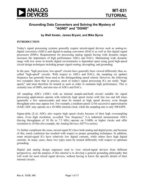
INTRODUCTION<br />
<strong>Grounding</strong> <strong>Data</strong> <strong>Converters</strong> <strong>and</strong> <strong>Solving</strong> the Mystery of<br />
"AGND" <strong>and</strong> "DGND"<br />
by Walt Kester, James Bryant, <strong>and</strong> Mike Byrne<br />
Rev.A, 10/08, WK Page 1 of 17<br />
<strong>MT</strong>-<strong>031</strong><br />
TUTORIAL<br />
Today's signal processing systems generally require mixed-signal devices such as analog-todigital<br />
converters (ADCs) <strong>and</strong> digital-to-analog converters (DACs) as well as fast digital signal<br />
processors (DSPs). Requirements for processing analog signals having wide dynamic ranges<br />
increases the importance of high performance ADCs <strong>and</strong> DACs. Maintaining wide dynamic<br />
range with low noise in hostile digital environments is dependent upon using good high-speed<br />
circuit design techniques including proper signal routing, decoupling, <strong>and</strong> grounding.<br />
In the past, "high precision, low-speed" circuits have generally been viewed differently than socalled<br />
"high-speed" circuits. With respect to ADCs <strong>and</strong> DACs, the sampling (or update)<br />
frequency has generally been used as the distinguishing speed criteria. However, the following<br />
two examples show that in practice, most of today's signal processing ICs are really "highspeed,"<br />
<strong>and</strong> must therefore be treated as such in order to maintain high performance. This is<br />
certainly true of DSPs, <strong>and</strong> also true of ADCs <strong>and</strong> DACs.<br />
All sampling ADCs (ADCs with an internal sample-<strong>and</strong>-hold circuit) suitable for signal<br />
processing applications operate with relatively high speed clocks with fast rise <strong>and</strong> fall times<br />
(generally a few nanoseconds) <strong>and</strong> must be treated as high speed devices, even though<br />
throughput rates may appear low. For example, a medium-speed 12-bit successive approximation<br />
(SAR) ADC may operate on a 10-MHz internal clock, while the sampling rate is only 500 kSPS.<br />
Sigma-delta (Σ-Δ) ADCs also require high speed clocks because of their high oversampling<br />
ratios. Even high resolution, so-called "low frequency" Σ-Δ industrial measurement ADCs<br />
(having throughputs of 10 Hz to 7.5 kHz) operate on 5-MHz or higher clocks <strong>and</strong> offer<br />
resolution to 24-bits (for example, the <strong>Analog</strong> <strong>Devices</strong> AD77xx-series).<br />
To further complicate the issue, mixed-signal ICs have both analog <strong>and</strong> digital ports, <strong>and</strong> because<br />
of this, much confusion has resulted with respect to proper grounding techniques. In addition,<br />
some mixed-signal ICs have relatively low digital currents, while others have high digital<br />
currents. In many cases, these two types must be treated differently with respect to optimum<br />
grounding.<br />
Digital <strong>and</strong> analog design engineers tend to view mixed-signal devices from different<br />
perspectives, <strong>and</strong> the purpose of this tutorial is to develop a general grounding philosophy that<br />
will work for most mixed signal devices, without having to know the specific details of their<br />
internal circuits.
GROUND AND POWER PLANES<br />
<strong>MT</strong>-<strong>031</strong><br />
The importance of maintaining a low impedance large area ground plane is critical to all analog<br />
<strong>and</strong> digital circuits today. The ground plane not only acts as a low impedance return path for<br />
decoupling high frequency currents (caused by fast digital logic) but also minimizes EMI/RFI<br />
emissions. Because of the shielding action of the ground plane, the circuit's susceptibility to<br />
external EMI/RFI is also reduced.<br />
Ground planes also allow the transmission of high speed digital or analog signals using<br />
transmission line techniques (microstrip or stripline) where controlled impedances are required.<br />
The use of "buss wire" is totally unacceptable as a "ground" because of its impedance at the<br />
equivalent frequency of most logic transitions. For instance, #22 gauge wire has about 20<br />
nH/inch inductance. A transient current having a slew rate of 10 mA/ns created by a logic signal<br />
would develop an unwanted voltage drop of 200 mV at this frequency flowing through 1 inch of<br />
this wire:<br />
Δi<br />
10 mA<br />
Δ v = L = 20 nH × = 200 mV.<br />
Eq. 1<br />
Δt<br />
ns<br />
For a signal having a 2-V peak-to-peak range, this translates into an error of about<br />
10% (approximately 3.5-bit accuracy). Even in all-digital circuits, this error would result in<br />
considerable degradation of logic noise margins.<br />
Figure 1 shows the classic illustration of a situation where the digital return current modulates<br />
the analog return current (top figure). The ground return wire inductance <strong>and</strong> resistance is shared<br />
between the analog <strong>and</strong> digital circuits, <strong>and</strong> this is what causes the interaction <strong>and</strong> resulting error.<br />
A possible solution is to make the digital return current path flow directly to the GND REF as<br />
shown in the bottom figure. This is the fundamental concept of a "star," or single-point ground<br />
system. Implementing the true single-point ground in a system which contains multiple high<br />
frequency return paths is difficult because the physical length of the individual return current<br />
wires will introduce parasitic resistance <strong>and</strong> inductance which can make obtaining a low<br />
impedance high frequency ground difficult. In practice, the current returns must consist of large<br />
area ground planes for low impedance to high frequency currents. Without a low-impedance<br />
ground plane, it is therefore almost impossible to avoid these shared impedances, especially at<br />
high frequencies.<br />
Page 2 of 17
+ +<br />
VD VA V D<br />
GND<br />
REF<br />
+ +<br />
VA GND<br />
REF<br />
V IN<br />
V IN<br />
I D<br />
I A<br />
I A + I D<br />
I D<br />
I A<br />
ANALOG<br />
CIRCUITS<br />
ANALOG<br />
CIRCUITS<br />
I A<br />
I D<br />
I D<br />
DIGITAL<br />
CIRCUITS<br />
DIGITAL<br />
CIRCUITS<br />
<strong>MT</strong>-<strong>031</strong><br />
INCORRECT<br />
CORRECT<br />
Figure 1: Digital Currents Flowing in <strong>Analog</strong> Return Path Create Error Voltages<br />
All integrated circuit ground pins should be soldered directly to the low-impedance ground plane<br />
to minimize series inductance <strong>and</strong> resistance. The use of traditional IC sockets is not<br />
recommended with high-speed devices. The extra inductance <strong>and</strong> capacitance of even "low<br />
profile" sockets may corrupt the device performance by introducing unwanted shared paths. If<br />
sockets must be used with DIP packages, as in prototyping, individual "pin sockets" or "cage<br />
jacks" may be acceptable. Both capped <strong>and</strong> uncapped versions of these pin sockets are available<br />
(AMP part numbers 5-330808-3, <strong>and</strong> 5-330808-6). They have spring-loaded gold contacts which<br />
make good electrical <strong>and</strong> mechanical connection to the IC pins. Multiple insertions, however,<br />
may degrade their performance.<br />
LOW AND HIGH FREQUENCY DECOUPLING<br />
Each power supply should be decoupled to the low-impedance ground plane with a high quality<br />
electrolytic capacitor at the point it enters the PC board. This minimizes low frequency noise on<br />
the supply runs. At each individual analog stage, further local, high-frequency-only filtering is<br />
required at the individual IC package power pins.<br />
Figure 2 shows this technique, in both correct (left) as well as incorrect example<br />
implementations (right). In the left example, a typical 0.1-μF chip ceramic capacitor goes<br />
directly to the opposite PCB side ground plane, by virtue of the via, <strong>and</strong> on to the IC's GND pin<br />
by a second via. In contrast, the less desirable setup at the right adds additional PCB trace<br />
inductance in the ground path of the decoupling cap, reducing effectiveness.<br />
Page 3 of 17
CORRECT INCORRECT<br />
OPTIONAL<br />
FERRITE BEADS<br />
POWER<br />
SUPPLY<br />
TRACE<br />
IC<br />
V+<br />
GND<br />
DECOUPLING<br />
CAPACITOR<br />
VIAS TO<br />
GROUND<br />
PLANE<br />
POWER<br />
SUPPLY<br />
TRACE<br />
IC<br />
V+<br />
GND<br />
DECOUPLING<br />
CAPACITOR<br />
PCB<br />
TRACE<br />
VIA TO<br />
GROUND<br />
PLANE<br />
<strong>MT</strong>-<strong>031</strong><br />
Figure 2: Localized High Frequency Supply Filter(s) Provides Optimum Filtering<br />
<strong>and</strong> Decoupling Via Short Low-Inductance Path (Ground Plane)<br />
All high frequency (i.e., ≥10 MHz) ICs should use a bypassing scheme similar to Figure 2 for<br />
best performance. The ferrite beads aren't 100% necessary, but they will add extra high<br />
frequency noise isolation <strong>and</strong> decoupling, which is often desirable. Possible caveats here would<br />
be to verify that the beads never saturate, when the ICs are h<strong>and</strong>ling high currents.<br />
Note that with some ferrites, even before full saturation occurs, some beads can be non-linear, so<br />
if a power stage is required to operate with a low distortion output, this should also be checked.<br />
DOUBLE-SIDED VS. MULTILAYER PRINTED CIRCUIT BOARDS<br />
Each PCB in the system should have at least one complete layer dedicated to the ground plane.<br />
Ideally, a double-sided board should have one side completely dedicated to ground <strong>and</strong> the other<br />
side for interconnections. In practice, this is not possible, since some of the ground plane will<br />
certainly have to be removed to allow for signal <strong>and</strong> power crossovers, vias, <strong>and</strong> through-holes.<br />
Nevertheless, as much area as possible should be preserved, <strong>and</strong> at least 75% should remain.<br />
After completing an initial layout, the ground layer should be checked carefully to make sure<br />
there are no isolated ground "isl<strong>and</strong>s," because IC ground pins located in a ground "isl<strong>and</strong>" have<br />
no current return path to the ground plane. Also, the ground plane should be checked for<br />
"skinny" connections between adjacent large areas which may significantly reduce the<br />
effectiveness of the ground plane. Needless to say, auto-routing board layout techniques will<br />
generally lead to a layout disaster on a mixed-signal board, so manual intervention is highly<br />
recommended.<br />
Systems that are densely packed with surface mount ICs will have a large number of<br />
interconnections; therefore multilayer boards are m<strong>and</strong>atory. This allows at least one complete<br />
layer to be dedicated to ground. A simple 4-layer board would have internal ground <strong>and</strong> power<br />
plane layers with the outer two layers used for interconnections between the surface mount<br />
components. Placing the power <strong>and</strong> ground planes adjacent to each other provides additional<br />
Page 4 of 17
<strong>MT</strong>-<strong>031</strong><br />
inter-plane capacitance which helps high frequency decoupling of the power supply. In most<br />
systems, 4-layers are not enough, <strong>and</strong> additional layers are required for routing signals as well as<br />
power.<br />
MULTICARD MIXED-SIGNAL SYSTEMS<br />
The best way of minimizing ground impedance in a multicard system is to use a "motherboard"<br />
PCB as a backplane for interconnections between cards, thus providing a continuous ground<br />
plane to the backplane. The PCB connector should have at least 30-40% of its pins devoted to<br />
ground, <strong>and</strong> these pins should be connected to the ground plane on the backplane motherboard.<br />
To complete the overall system grounding scheme there are two possibilities:<br />
1. The backplane ground plane can be connected to chassis ground at numerous points,<br />
thereby diffusing the various ground current return paths. This is commonly referred to as<br />
a "multipoint" grounding system <strong>and</strong> is shown in Figure 3.<br />
2. The ground plane can be connected to a single system "star ground" point (generally at<br />
the power supply).<br />
The first approach is most often used in all-digital systems, but can be used in mixed-signal<br />
systems provided the ground currents due to digital circuits are sufficiently low <strong>and</strong> diffused over<br />
a large area. The low ground impedance is maintained all the way through the PC boards, the<br />
backplane, <strong>and</strong> ultimately the chassis. However, it is critical that good electrical contact be made<br />
where the grounds are connected to the sheet metal chassis. This requires self-tapping sheet<br />
metal screws or "biting" washers. Special care must be taken where anodized aluminum is used<br />
for the chassis material, since its surface acts as an insulator.<br />
V A<br />
PCB<br />
GROUND PLANE<br />
CHASSIS<br />
GROUND<br />
V D<br />
GROUND PLANE<br />
V A<br />
PCB<br />
GROUND PLANE<br />
POWER<br />
SUPPLIES<br />
Figure 3: Multipoint Ground Concept<br />
Page 5 of 17<br />
V D<br />
BACKPLANE<br />
V A<br />
V D
<strong>MT</strong>-<strong>031</strong><br />
The second approach ("star ground") is often used in high speed mixed-signal systems having<br />
separate analog <strong>and</strong> digital ground systems <strong>and</strong> warrants further discussion.<br />
SEPARATING ANALOG AND DIGITAL GROUND PLANES<br />
In mixed-signal systems with large amounts of digital circuitry, it is highly desirable to<br />
physically separate sensitive analog components from noisy digital components. It may also be<br />
beneficial to use separate ground planes for the analog <strong>and</strong> the digital circuitry. These planes<br />
should not overlap in order to minimize capacitive coupling between the two. The separate<br />
analog <strong>and</strong> digital ground planes are continued on the backplane using either motherboard<br />
ground planes or "ground screens" which are made up of a series of wired interconnections<br />
between the connector ground pins. The arrangement shown in Figure 4 illustrates that the two<br />
planes are kept separate all the way back to a common system "star" ground, generally located at<br />
the power supplies. The connections between the ground planes, the power supplies, <strong>and</strong> the<br />
"star" should be made up of multiple bus bars or wide copper braids for minimum resistance <strong>and</strong><br />
inductance. The back-to-back Schottky diodes on each PCB are inserted to prevent accidental dc<br />
voltage from developing between the two ground systems when cards are plugged <strong>and</strong><br />
unplugged. This voltage should be kept less than 300 mV to prevent damage to ICs which have<br />
connections to both the analog <strong>and</strong> digital ground planes. Schottky diodes are preferable because<br />
of their low capacitance <strong>and</strong> low forward voltage drop. The low capacitance prevents ac coupling<br />
between the analog <strong>and</strong> digital ground planes. Schottky diodes begin to conduct at about 300<br />
mV, <strong>and</strong> several parallel diodes in parallel may be required if high currents are expected. In some<br />
cases, ferrite beads can be used instead of Schottky diodes, however they introduce dc ground<br />
loops which can be troublesome in precision systems.<br />
V A<br />
ANALOG<br />
GROUND<br />
PLANE<br />
DIGITAL<br />
GROUND<br />
PLANE<br />
A D<br />
ANALOG GROUND PLANE<br />
PCB PCB<br />
SYSTEM<br />
STAR<br />
GROUND<br />
V D<br />
DIGITAL GROUND PLANE<br />
V A<br />
ANALOG<br />
GROUND<br />
PLANE<br />
POWER<br />
SUPPLIES<br />
DIGITAL<br />
GROUND<br />
PLANE<br />
A D<br />
BACKPLANE<br />
Figure 4: Separating <strong>Analog</strong> <strong>and</strong> Digital Ground Planes<br />
Page 6 of 17<br />
V D<br />
V A<br />
V D
<strong>MT</strong>-<strong>031</strong><br />
It is m<strong>and</strong>atory that the impedance of the ground planes be kept as low as possible, all the way<br />
back to the system star ground. DC or ac voltages of more than 300 mV between the two ground<br />
planes can not only damage ICs but cause false triggering of logic gates <strong>and</strong> possible latchup.<br />
GROUNDING AND DECOUPLING MIXED-SIGNAL ICs WITH LOW<br />
DIGITALCURRENTS<br />
Sensitive analog components such as amplifiers <strong>and</strong> voltage references are always referenced<br />
<strong>and</strong> decoupled to the analog ground plane. The ADCs <strong>and</strong> DACs (<strong>and</strong> other mixed-signal ICs)<br />
with low digital currents should generally be treated as analog components <strong>and</strong> also grounded<br />
<strong>and</strong> decoupled to the analog ground plane. At first glance, this may seem somewhat<br />
contradictory, since a converter has an analog <strong>and</strong> digital interface <strong>and</strong> usually has pins<br />
designated as analog ground (AGND) <strong>and</strong> digital ground (DGND). The diagram shown in<br />
Figure 5 will help to explain this seeming dilemma.<br />
A<br />
AIN/<br />
OUT<br />
L P<br />
R P<br />
ANALOG<br />
CIRCUITS<br />
VA FERRITE BEAD<br />
V A<br />
C STRAY<br />
V D<br />
DIGITAL<br />
CIRCUITS<br />
A B<br />
R P<br />
L P<br />
C STRAY<br />
I A<br />
AGND DGND<br />
SHORT<br />
I D<br />
L P<br />
R P<br />
R P<br />
L P<br />
DATA<br />
R<br />
SEE<br />
TEXT<br />
BUFFER<br />
GATE OR<br />
REGISTER<br />
A<br />
CONNECTIONS<br />
A VNOISE D<br />
A = ANALOG GROUND PLANE D = DIGITAL GROUND PLANE<br />
V D<br />
C IN ≈ 10pF<br />
D<br />
DATA<br />
BUS<br />
Figure 5: Proper <strong>Grounding</strong> of Mixed-signal ICs With Low Internal Digital Currents<br />
Inside an IC that has both analog <strong>and</strong> digital circuits, such as an ADC or a DAC, the grounds are<br />
usually kept separate to avoid coupling digital signals into the analog circuits. Figure 5 shows a<br />
simple model of a converter. There is nothing the IC designer can do about the wirebond<br />
inductance <strong>and</strong> resistance associated with connecting the bond pads on the chip to the package<br />
pins except to realize it's there. The rapidly changing digital currents produce a voltage at point B<br />
which will inevitably couple into point A of the analog circuits through the stray capacitance,<br />
C STRAY . In addition, there is approximately 0.2-pF unavoidable stray capacitance between<br />
every pin of the IC package! It's the IC designer's job to make the chip work in spite of this.<br />
However, in order to prevent further coupling, the AGND <strong>and</strong> DGND pins should be joined<br />
Page 7 of 17
<strong>MT</strong>-<strong>031</strong><br />
together externally to the analog ground plane with minimum lead lengths. Any extra impedance<br />
in the DGND connection will cause more digital noise to be developed at point B; it will, in turn,<br />
couple more digital noise into the analog circuit through the stray capacitance. Note that<br />
connecting DGND to the digital ground plane applies V NOISE across the AGND <strong>and</strong> DGND<br />
pins <strong>and</strong> invites disaster!<br />
The name "DGND" on an IC tells us that this pin connects to the digital ground of the IC. This<br />
does not imply that this pin must be connected to the digital ground of the system.<br />
It is true that this arrangement may inject a small amount of digital noise onto the analog ground<br />
plane. These currents should be quite small, <strong>and</strong> can be minimized by ensuring that the converter<br />
output does not drive a large fanout (they normally can't, by design). Minimizing the fanout on<br />
the converter's digital port will also keep the converter logic transitions relatively free from<br />
ringing <strong>and</strong> minimize digital switching currents, <strong>and</strong> thereby reducing any potential coupling into<br />
the analog port of the converter. The logic supply pin (VD ) can be further isolated from the<br />
analog supply by the insertion of a small lossy ferrite bead as shown in Figure 5. The internal<br />
transient digital currents of the converter will flow in the small loop from VD through the<br />
decoupling capacitor <strong>and</strong> to DGND (this path is shown with a heavy line on the diagram). The<br />
transient digital currents will therefore not appear on the external analog ground plane, but are<br />
confined to the loop. The VD pin decoupling capacitor should be mounted as close to the<br />
converter as possible to minimize parasitic inductance. These decoupling capacitors should be<br />
low inductance ceramic types, typically between 0.01 µF <strong>and</strong> 0.1 µF.<br />
TREAT THE ADC DIGITAL OUTPUTS WITH CARE<br />
It is always a good idea (as shown in Figure 5) to place a buffer register adjacent to the converter<br />
to isolate the converter's digital lines from noise on the data bus. The register also serves to<br />
minimize loading on the digital outputs of the converter <strong>and</strong> acts as a Faraday shield between the<br />
digital outputs <strong>and</strong> the data bus. Even though many converters have three-state outputs/inputs,<br />
this isolation register still represents good design practice. In some cases it may be desirable to<br />
add an additional buffer register on the analog ground plane next to the converter output to<br />
provide greater isolation.<br />
The series resistors (labeled "R" in Figure 5) between the ADC output <strong>and</strong> the buffer register<br />
input help to minimize the digital transient currents which may affect converter performance.<br />
The resistors isolate the digital output drivers from the capacitance of the buffer register inputs.<br />
In addition, the RC network formed by the series resistor <strong>and</strong> the buffer register input<br />
capacitance acts as a lowpass filter to slow down the fast edges.<br />
A typical CMOS gate combined with PCB trace <strong>and</strong> a through-hole will create a load of<br />
approximately 10 pF. A logic output slew rate of 1 V/ns will produce 10 mA of dynamic current<br />
if there is no isolation resistor:<br />
Δv<br />
1 V<br />
Δ I = C = 10 pF × = 10 mA . Eq. 2<br />
Δt<br />
ns<br />
Page 8 of 17
<strong>MT</strong>-<strong>031</strong><br />
A 500-Ω series resistors will minimize this output current <strong>and</strong> result in a rise <strong>and</strong> fall time of<br />
approximately 11 ns when driving the 10-pF input capacitance of the register:<br />
t r<br />
= 2.<br />
2 × τ = 2.<br />
2 × R ⋅C<br />
= 2.<br />
2 × 500 Ω × 10 pF = 11 ns.<br />
Eq. 3<br />
TTL registers should be avoided, since they can appreciably add to the dynamic switching<br />
currents because of their higher input capacitance.<br />
The buffer register <strong>and</strong> other digital circuits should be grounded <strong>and</strong> decoupled to the digital<br />
ground plane of the PC board. Notice that any noise between the analog <strong>and</strong> digital ground plane<br />
reduces the noise margin at the converter digital interface. Since digital noise immunity is of the<br />
orders of hundreds or thous<strong>and</strong>s of millivolts, this is unlikely to matter. The analog ground plane<br />
will generally not be very noisy, but if the noise on the digital ground plane (relative to the<br />
analog ground plane) exceeds a few hundred millivolts, then steps should be taken to reduce the<br />
digital ground plane impedance, thereby maintaining the digital noise margins at an acceptable<br />
level. Under no circumstances should the voltage between the two ground planes exceed 300<br />
mV, or the ICs may be damaged.<br />
Separate power supplies for analog <strong>and</strong> digital circuits are also highly desirable, even if the<br />
voltages are the same. The analog supply should be used to power the converter. If the converter<br />
has a pin designated as a digital supply pin (V D ), it should either be powered from a separate<br />
analog supply, or filtered as shown in the diagram. All converter power pins should be decoupled<br />
to the analog ground plane, <strong>and</strong> all logic circuit power pins should be decoupled to the digital<br />
ground plane as shown in Figure 6.<br />
A<br />
A<br />
A<br />
AMP<br />
V A<br />
V A<br />
VOLTAGE<br />
REFERENCE<br />
A<br />
V A<br />
V A<br />
A A<br />
FERRITE<br />
BEAD<br />
ADC<br />
OR<br />
DAC<br />
V D<br />
AGND DGND<br />
A A<br />
SAMPLING<br />
CLOCK<br />
GENERATOR<br />
A<br />
V A<br />
R<br />
R<br />
SEE<br />
TEXT<br />
A<br />
V D<br />
BUFFER<br />
GATE<br />
OR<br />
REGISTER<br />
Figure 6: <strong>Grounding</strong> <strong>and</strong> Decoupling Points<br />
Page 9 of 17<br />
D<br />
D<br />
D<br />
TO OTHER<br />
DIGITAL<br />
CIRCUITS<br />
ANALOG<br />
GROUND PLANE<br />
DIGITAL<br />
GROUND PLANE
<strong>MT</strong>-<strong>031</strong><br />
In some cases it may not be possible to connect V D to the analog supply. Some of the newer,<br />
high speed ICs may have their analog circuits powered by +5 V, but the digital interface powered<br />
by +3 V to interface to 3 V logic. In this case, the +3 V pin of the IC should be decoupled<br />
directly to the analog ground plane. It is also advisable to connect a ferrite bead in series with the<br />
power trace that connects the pin to the +3 V digital logic supply.<br />
The sampling clock generation circuitry should be treated like analog circuitry <strong>and</strong> also be<br />
grounded <strong>and</strong> heavily-decoupled to the analog ground plane. Phase noise on the sampling clock<br />
produces degradation in system SNR as will be discussed shortly.<br />
SAMPLING CLOCK CONSIDERATIONS<br />
In a high performance sampled data system a low phase-noise oscillator should be used to<br />
generate the ADC (or DAC) sampling clock because sampling clock jitter modulates the analog<br />
input/output signal <strong>and</strong> raises the noise <strong>and</strong> distortion floor. The sampling clock generator should<br />
be isolated from noisy digital circuits <strong>and</strong> grounded <strong>and</strong> decoupled to the analog ground plane, as<br />
is true for the op amp <strong>and</strong> the ADC.<br />
The effect of sampling clock jitter on ADC signal-to-noise ratio (SNR) is given approximately<br />
by the equation:<br />
⎡ 1 ⎤<br />
SNR = 20log10<br />
⎢ ⎥ , Eq. 4<br />
⎢⎣<br />
2πft<br />
j ⎥⎦<br />
where SNR is the SNR of a perfect ADC of infinite resolution where the only source of noise is<br />
that caused by the rms sampling clock jitter, t j . Note that f in the above equation is the analog<br />
input frequency. Just working through a simple example, if t j = 50 ps rms, f = 100 kHz, then<br />
SNR = 90 dB, equivalent to about 15-bit dynamic range. This effect of clock jitter on SNR is<br />
discussed in much more detail in Tutorial <strong>MT</strong>-007.<br />
It should be noted that t j in the above example is the root-sum-square (rss) value of the external<br />
clock jitter <strong>and</strong> the internal ADC clock jitter (called aperture jitter). However, in most high<br />
performance ADCs, the internal aperture jitter is negligible compared to the jitter on the<br />
sampling clock.<br />
Ideally, the sampling clock oscillator should be referenced to the analog ground plane in a splitground<br />
system. However, this is not always possible because of system constraints. In many<br />
cases, the sampling clock must be derived from a higher frequency multi-purpose system clock<br />
which is generated on the digital ground plane. It must then pass from its origin on the digital<br />
ground plane to the ADC on the analog ground plane. Ground noise between the two planes adds<br />
directly to the clock signal <strong>and</strong> will produce excess jitter. The jitter can cause degradation in the<br />
signal-to-noise ratio <strong>and</strong> also produce unwanted harmonics.<br />
Page 10 of 17
<strong>MT</strong>-<strong>031</strong><br />
This can be remedied somewhat by transmitting the sampling clock signal as a differential signal<br />
using either a small RF transformer as shown in Figure 7 or a high speed differential driver <strong>and</strong><br />
receiver IC. Many high-speed ADCs have differential sampling clock inputs to facilitate this<br />
approach. If an active differential driver <strong>and</strong> receiver are used, they should be ECL, low-level<br />
ECL, or LVDS to minimize phase jitter. In a single +5 V supply system, ECL logic can be<br />
connected between ground <strong>and</strong> +5 V (PECL), <strong>and</strong> the outputs ac coupled into the ADC sampling<br />
clock input. In either case, the original master system clock must be generated from a low phase<br />
noise oscillator, <strong>and</strong> not the clock output of a DSP, microprocessor, or microcontroller.<br />
In order to facilitate system clock management, a family clock generation <strong>and</strong> distribution<br />
products is available from <strong>Analog</strong> <strong>Devices</strong> as well as a complete selection of phase-locked loops<br />
(PLLs).<br />
V D<br />
LOW PHASE<br />
NOISE<br />
MASTER CLOCK<br />
D VD D<br />
V D<br />
SYSTEM CLOCK<br />
GENERATORS<br />
DSP OR MICROPROCESSOR<br />
D<br />
SNR = 20 log 10<br />
DIGITAL GROUND PLANE ANALOG GROUND PLANE<br />
1<br />
2π 2π f t j<br />
V D<br />
D A<br />
+<br />
_<br />
V A<br />
D A<br />
t j = Sampling Clock Jitter<br />
f = <strong>Analog</strong> Input Frequency<br />
SAMPLING<br />
CLOCK<br />
METHOD 1<br />
SAMPLING<br />
CLOCK<br />
METHOD 2<br />
Figure 7: Sampling Clock Distribution From Digital to <strong>Analog</strong> Ground Planes<br />
THE ORIGINS OF THE CONFUSION ABOUT MIXED-SIGNAL GROUNDING:<br />
APPLYING SINGLE-CARD GROUNDING CONCEPTS TO MULTICARD SYSTEMS<br />
Most ADC, DAC, <strong>and</strong> other mixed-signal device data sheets discuss grounding relative to a<br />
single PCB, usually the manufacturer's own evaluation board. This has been a source of<br />
confusion when trying to apply these principles to multicard or multi-ADC/DAC systems. The<br />
recommendation is usually to split the PCB ground plane into an analog plane <strong>and</strong> a digital<br />
plane. It is then further recommended that the AGND <strong>and</strong> DGND pins of a converter be tied<br />
together <strong>and</strong> that the analog ground plane <strong>and</strong> digital ground planes be connected at that same<br />
point as shown in Figure 8. This essentially creates the system "star" ground at the mixed-signal<br />
device.<br />
Page 11 of 17
<strong>MT</strong>-<strong>031</strong><br />
All noisy digital currents flow through the digital power supply to the digital ground plane <strong>and</strong><br />
back to the digital supply; they are isolated from the sensitive analog portion of the board. The<br />
system star ground occurs where the analog <strong>and</strong> digital ground planes are joined together at the<br />
mixed signal device. While this approach will generally work in a simple system with a single<br />
PCB <strong>and</strong> single ADC/DAC, it is not usually optimum for multicard mixed-signal systems. In<br />
systems having several ADCs or DACs on different PCBs (or on the same PCB, for that matter),<br />
the analog <strong>and</strong> digital ground planes become connected at several points, creating the possibility<br />
of ground loops <strong>and</strong> making a single-point "star" ground system impossible. For these reasons,<br />
this grounding approach is not recommended for multicard systems, <strong>and</strong> the approach previously<br />
discussed should be used for mixed signal ICs with low digital currents.<br />
SYSTEM<br />
STAR<br />
GROUND<br />
ANALOG<br />
CIRCUITS<br />
V A<br />
ANALOG<br />
GROUND PLANE<br />
ANALOG<br />
SUPPLY<br />
VA VD MIXED<br />
SIGNAL<br />
DEVICE<br />
AGND DGND<br />
A A D D<br />
A<br />
D<br />
V D<br />
DIGITAL<br />
CIRCUITS<br />
DIGITAL<br />
GROUND PLANE<br />
DIGITAL<br />
SUPPLY<br />
Figure 8: <strong>Grounding</strong> Mixed Signal ICs : Single PC Board (Typical Evaluation/Test<br />
Board)<br />
SUMMARY: GROUNDING MIXED SIGNAL DEVICES WITH LOW DIGITAL<br />
CURRENTS IN A MULTICARD SYSTEM<br />
Figure 9 summarizes the approach previously described for grounding a mixed signal device<br />
which has low digital currents. The analog ground plane is not corrupted because the small<br />
digital transient currents flow in the small loop between V D , the decoupling capacitor, <strong>and</strong><br />
DGND (shown as a heavy line). The mixed signal device is for all intents <strong>and</strong> purposes treated as<br />
an analog component. The noise VN between the ground planes reduces the noise margin at the<br />
digital interface but is generally not harmful if kept less than 300 mV by using a low impedance<br />
digital ground plane all the way back to the system star ground.<br />
Page 12 of 17
<strong>MT</strong>-<strong>031</strong><br />
However, mixed signal devices such as sigma-delta ADCs, codecs, <strong>and</strong> DSPs with on-chip<br />
analog functions are becoming more <strong>and</strong> more digitally intensive. Along with the additional<br />
digital circuitry come larger digital currents <strong>and</strong> noise. For example, a sigma-delta ADC or DAC<br />
contains a complex digital filter which adds considerably to the digital current in the device. The<br />
method previously discussed depends on the decoupling capacitor between V D <strong>and</strong> DGND to<br />
keep the digital transient currents isolated in a small loop. However, if the digital currents are<br />
significant enough <strong>and</strong> have components at dc or low frequencies, the decoupling capacitor may<br />
have to be so large that it is impractical. Any digital current which flows outside the loop<br />
between V D <strong>and</strong> DGND must flow through the analog ground plane. This may degrade<br />
performance, especially in high resolution systems.<br />
ANALOG<br />
CIRCUITS<br />
TO SYSTEM<br />
ANALOG SUPPLY<br />
V A<br />
VA MIXED<br />
SIGNAL<br />
DEVICE<br />
AGND DGND<br />
A A A<br />
D D<br />
ANALOG<br />
GROUND PLANE<br />
A A<br />
FILTER<br />
V D<br />
V N<br />
R<br />
V D<br />
BUFFER<br />
LATCH<br />
DIGITAL<br />
CIRCUITS<br />
DIGITAL<br />
GROUND PLANE<br />
D D<br />
TO SYSTEM STAR GROUND<br />
V N = NOISE BETWEEN<br />
GROUND PLANES<br />
BUS<br />
TO SYSTEM<br />
DIGITAL SUPPLY<br />
Figure 9: <strong>Grounding</strong> Mixed Signal ICs with Low Internal Digital Currents:<br />
Multiple PC Boards<br />
It is difficult to predict what level of digital current flowing into the analog ground plane will<br />
become unacceptable in a system. All we can do at this point is to suggest an alternative<br />
grounding method which may yield better performance.<br />
SUMMARY: GROUNDING MIXED SIGNAL DEVICES WITH HIGH DIGITAL<br />
CURRENTS IN A MULTICARD SYSTEM (USE THIS METHOD WITH CAUTION!)<br />
An alternative grounding method for a mixed signal device with high levels of digital currents is<br />
shown in Figure 10. The AGND of the mixed signal device is connected to the analog ground<br />
plane, <strong>and</strong> the DGND of the device is connected to the digital ground plane. The digital currents<br />
are isolated from the analog ground plane, but the noise between the two ground planes is<br />
applied directly between the AGND <strong>and</strong> DGND pins of the device. For this method to be<br />
successful, the analog <strong>and</strong> digital circuits within the mixed signal device must be well isolated.<br />
Page 13 of 17
<strong>MT</strong>-<strong>031</strong><br />
The noise between AGND <strong>and</strong> DGND pins must not be large enough to reduce internal noise<br />
margins or cause corruption of the internal analog circuits.<br />
Figure 10 shows optional Schottky diodes (back-to-back) or a ferrite bead connecting the analog<br />
<strong>and</strong> digital ground planes. The Schottky diodes prevent large dc voltages or low frequency<br />
voltage spikes from developing across the two planes. These voltages can potentially damage the<br />
mixed signal IC if they exceed 300 mV because they appear directly between the AGND <strong>and</strong><br />
DGND pins. As an alternative to the back-to-back Schottky diodes, a ferrite bead provides a dc<br />
connection between the two planes but isolates them at frequencies above a few MHz where the<br />
ferrite bead becomes resistive. This protects the IC from dc voltages between AGND <strong>and</strong><br />
DGND, but the dc connection provided by the ferrite bead can introduce unwanted dc ground<br />
loops <strong>and</strong> may not be suitable for high resolution systems.<br />
<br />
BACK-TO-BACK<br />
SCHOTTKY<br />
DIODES<br />
OR<br />
FERRITE<br />
BEAD<br />
(SEE TEXT)<br />
TO SYSTEM<br />
ANALOG SUPPLY<br />
V A<br />
ANALOG<br />
CIRCUITS<br />
ANALOG<br />
GROUND PLANE<br />
V N<br />
VA VD MIXED<br />
SIGNAL<br />
DEVICE<br />
AGND DGND<br />
A A D D<br />
A A D D<br />
<br />
TO SYSTEM STAR GROUND<br />
VN = NOISE BETWEEN<br />
GROUND PLANES<br />
VD DIGITAL<br />
CIRCUITS<br />
DIGITAL<br />
GROUND PLANE<br />
TO SYSTEM<br />
DIGITAL SUPPLY<br />
Figure 10: <strong>Grounding</strong> Alternative for Mixed-Signal ICs with<br />
High Digital Currents: Multiple PC Boards<br />
Whenever AGND <strong>and</strong> DGND pins are separated in the special case of ICs with high digital<br />
currents, provisions should be made to connect them together if necessary. Jumpers <strong>and</strong>/or strap<br />
options allow both methods to be tried to verify which gives the best overall performance in the<br />
system.<br />
GROUNDING SUMMARY<br />
There is no single grounding method which will guarantee optimum performance 100% of the<br />
time! This section has presented a number of possible options depending upon the characteristics<br />
of the particular mixed signal devices in question. It is helpful, however, to provide for as many<br />
options as possible when laying out the initial PC board.<br />
Page 14 of 17
<strong>MT</strong>-<strong>031</strong><br />
It is m<strong>and</strong>atory that at least one layer of the PC board be dedicated to ground plane! The initial<br />
board layout should provide for non-overlapping analog <strong>and</strong> digital ground planes, but pads <strong>and</strong><br />
vias should be provided at several locations for the installation of back-to-back Schottky diodes<br />
or ferrite beads, if required. It is also extremely important that pads <strong>and</strong> vias be provided so that<br />
the analog <strong>and</strong> digital ground planes can be connected together with jumpers if required. It is<br />
difficult to predict whether the "multi-point" (single ground plane) or the "star" ground (separate<br />
analog <strong>and</strong> digital ground planes) method will give best overall system performance; therefore,<br />
some experimentation with the final PC board using the jumpers may be required.<br />
When in doubt, it is always better to start out with a split analog <strong>and</strong> digital ground plane <strong>and</strong><br />
later connect them with jumpers, rather than to start out with a single ground plane <strong>and</strong> try <strong>and</strong><br />
later try <strong>and</strong> split it!<br />
SOME GENERAL PC BOARD LAYOUT GUIDELINES FOR MIXED-SIGNAL<br />
SYSTEMS<br />
It is evident that noise can be minimized by paying attention to the system layout <strong>and</strong> preventing<br />
different signals from interfering with each other. High level analog signals should be separated<br />
from low level analog signals, <strong>and</strong> both should be kept away from digital signals. We have seen<br />
elsewhere that in waveform sampling <strong>and</strong> reconstruction systems the sampling clock (which is a<br />
digital signal) is as vulnerable to noise as any analog signal, but is as liable to cause noise as any<br />
digital signal, <strong>and</strong> so must be kept isolated from both analog <strong>and</strong> digital systems. If clock driver<br />
packages are used in clock distribution, only one frequency clock should be passed through a<br />
single package. Sharing drivers between clocks of different frequencies in the same package will<br />
produce excess jitter <strong>and</strong> crosstalk <strong>and</strong> degrade performance.<br />
The ground plane can act as a shield where sensitive signals cross. Figure 11 shows a good<br />
layout for a data acquisition board where all sensitive areas are isolated from each other <strong>and</strong><br />
signal paths are kept as short as possible. While real life is rarely as tidy as this, the principle<br />
remains a valid one.<br />
There are a number of important points to be considered when making signal <strong>and</strong> power<br />
connections. First of all a connector is one of the few places in the system where all signal<br />
conductors must run in parallel—it is therefore imperative to separate them with ground pins<br />
(creating a faraday shield) to reduce coupling between them.<br />
Multiple ground pins are important for another reason: they keep down the ground impedance at<br />
the junction between the board <strong>and</strong> the backplane. The contact resistance of a single pin of a<br />
PCB connector is quite low (of the order of 10 mΩ) when the board is new—as the board gets<br />
older the contact resistance is likely to rise, <strong>and</strong> the board's performance may be compromised. It<br />
is therefore well worthwhile to allocate extra PCB connector pins so that there are many ground<br />
connections (perhaps 30-40% of all the pins on the PCB connector should be ground pins). For<br />
similar reasons there should be several pins for each power connection, although there is no need<br />
to have as many as there are ground pins.<br />
Page 15 of 17
SAMPLING<br />
CLOCK GENERATOR<br />
REFERENCE ADC<br />
ANALOG DIGITAL<br />
FILTER<br />
POWER<br />
AMPLIFIER<br />
ANALOG<br />
INPUT<br />
MULTIPLE<br />
GROUNDS<br />
TIMING<br />
CIRCUITS<br />
BUFFER<br />
REGISTER<br />
DATA<br />
BUS<br />
DSP<br />
OR<br />
µP<br />
ADDRESS<br />
BUS<br />
Figure 11: <strong>Analog</strong> <strong>and</strong> Digital Circuits<br />
Should be Partitioned on PCB Layout<br />
CONTROL<br />
LOGIC<br />
DEMULTIPLEXER<br />
BUFFER<br />
MEMORY<br />
MULTIPLE<br />
GROUNDS<br />
<strong>MT</strong>-<strong>031</strong><br />
<strong>Analog</strong> <strong>Devices</strong> <strong>and</strong> other manufacturers of high performance mixed-signal ICs offer evaluation<br />
boards to assist customers in their initial evaluations <strong>and</strong> layout. ADC evaluation boards<br />
generally contain an on-board low-jitter sampling clock oscillator, output registers, <strong>and</strong><br />
appropriate power <strong>and</strong> signal connectors. They also may have additional support circuitry such<br />
as the ADC input buffer amplifier <strong>and</strong> external reference.<br />
The layout of the evaluation board is optimized in terms of grounding, decoupling, <strong>and</strong> signal<br />
routing <strong>and</strong> can be used as a model when laying out the ADC PC board in the system. The actual<br />
evaluation board layout is usually available from the ADC manufacturer in the form of computer<br />
CAD files (Gerber files). In many cases, the layout of the various layers appears on the data<br />
sheet for the device.<br />
Page 16 of 17
REFERENCES<br />
Page 17 of 17<br />
<strong>MT</strong>-<strong>031</strong><br />
1. Ralph Morrison, <strong>Grounding</strong> <strong>and</strong> Shielding Techniques, 4 th Edition, John Wiley, Inc., 1998, ISBN: 0471245186.<br />
2. Henry W. Ott, Noise Reduction Techniques in Electronic Systems, 2 nd Edition, John Wiley, Inc., 1988, ISBN: 0-<br />
471-85068-3.<br />
3. Paul Brokaw, "An IC Amplifier User's Guide to Decoupling, <strong>Grounding</strong> <strong>and</strong> Making Things Go Right for a<br />
Change", <strong>Analog</strong> <strong>Devices</strong> Application Note AN-202.<br />
4. Paul Brokaw <strong>and</strong> Jeff Barrow, "<strong>Grounding</strong> for Low- <strong>and</strong> High-Frequency Circuits," <strong>Analog</strong> <strong>Devices</strong><br />
Application Note AN-345.<br />
5. Howard W. Johnson <strong>and</strong> Martin Graham, High-Speed Digital Design, PTR Prentice Hall, 1993, ISBN:<br />
0133957241.<br />
6. Ralph Morrison, <strong>Solving</strong> Interference Problems in Electronics, John Wiley, 1995.<br />
7. Crystal Oscillators: MF Electronics, 10 Commerce Drive, New Rochelle, NY, 10801, 914-576-6570.<br />
8. Mark Montrose, EMC <strong>and</strong> the Printed Circuit Board, IEEE Press, 1999 (IEEE Order Number PC5756).<br />
9. John Ardizzoni, "A Practical Guide to High-Speed Printed-Circuit-Board Layout," <strong>Analog</strong> Dialogue, Vol. 39,<br />
Sept. 2005.<br />
10. Grant, Doug <strong>and</strong> Scott Wurcer, “Avoiding Passive-Component Pitfalls,” <strong>Analog</strong> <strong>Devices</strong> Application Note AN-<br />
348<br />
11. Walt Kester, <strong>Analog</strong>-Digital Conversion, <strong>Analog</strong> <strong>Devices</strong>, 2004, ISBN 0-916550-27-3, Chapter 9. Also<br />
available as The <strong>Data</strong> Conversion H<strong>and</strong>book, Elsevier/Newnes, 2005, ISBN 0-7506-7841-0, Chapter 9.<br />
Copyright 2009, <strong>Analog</strong> <strong>Devices</strong>, Inc. All rights reserved. <strong>Analog</strong> <strong>Devices</strong> assumes no responsibility for customer<br />
product design or the use or application of customers’ products or for any infringements of patents or rights of others<br />
which may result from <strong>Analog</strong> <strong>Devices</strong> assistance. All trademarks <strong>and</strong> logos are property of their respective holders.<br />
Information furnished by <strong>Analog</strong> <strong>Devices</strong> applications <strong>and</strong> development tools engineers is believed to be accurate<br />
<strong>and</strong> reliable, however no responsibility is assumed by <strong>Analog</strong> <strong>Devices</strong> regarding technical accuracy <strong>and</strong> topicality of<br />
the content provided in <strong>Analog</strong> <strong>Devices</strong> Tutorials.


