

ADF4251 Dual Fractional-N/Interger-N Frequency ... - Analog Devices
ADF4251 Dual Fractional-N/Interger-N Frequency ... - Analog Devices
ADF4251 Dual Fractional-N/Interger-N Frequency ... - Analog Devices

Create successful ePaper yourself
Turn your PDF publications into a flip-book with our unique Google optimized e-Paper software.
<strong>ADF4251</strong><br />
Phase <strong>Frequency</strong> Detector (PFD) and Charge Pump<br />
The PFD takes inputs from the R counter and N counter and<br />
produces an output proportional to the phase and frequency<br />
difference between them. Figure 6 is a simplified schematic. The<br />
PFD includes a delay element that controls the width of the<br />
antibacklash pulse. This pulse ensures that there is no dead zone<br />
in the PFD transfer function and minimizes phase noise and<br />
reference spurs.<br />
+IN<br />
–IN<br />
HI<br />
HI<br />
D1<br />
D2<br />
U1<br />
CLR1<br />
CLR2<br />
U2<br />
Q1<br />
Q2<br />
UP<br />
DELAY<br />
ELEMENT<br />
DOWN<br />
U3<br />
CHARGE<br />
PUMP<br />
Figure 6. PFD Simplified Schematic<br />
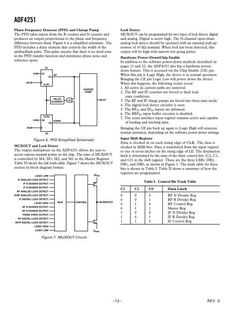
MUXOUT and Lock Detect<br />
The output multiplexer on the <strong>ADF4251</strong> allows the user to<br />
access various internal points on the chip. The state of MUXOUT<br />
is controlled by M4, M3, M2, and M1 in the Master Register.<br />
Table VI shows the full truth table. Figure 7 shows the MUXOUT<br />
section in block diagram format.<br />
LOGIC LOW<br />
IF ANALOG LOCK DETECT<br />
IF R DIVIDER OUTPUT<br />
IF N DIVIDER OUTPUT<br />
RF ANALOG LOCK DETECT<br />
IF/RF ANALOG LOCK DETECT<br />
IF DIGITAL LOCK DETECT<br />
LOGIC HIGH<br />
RF R DIVIDER OUTPUT<br />
RF N DIVIDER OUTPUT<br />
THREE STATE OUTPUT<br />
RF DIGITAL LOCK DETECT<br />
RF/IF DIGITAL LOCK DETECT<br />
LOGIC HIGH<br />
LOGIC LOW<br />
DV DD<br />
CP<br />
MUX CONTROL MUXOUT<br />
D GND<br />
Lock Detect<br />
MUXOUT can be programmed for two types of lock detect: digital<br />
and analog. Digital is active high. The N-channel open-drain<br />
analog lock detect should be operated with an external pull-up<br />
resistor of 10 kW nominal. When lock has been detected, this<br />
output will be high with narrow low going pulses.<br />
Hardware Power-Down/Chip Enable<br />
In addition to the software power-down methods described on<br />
pages 21 and 22, the <strong>ADF4251</strong> also has a hardware powerdown<br />
feature. This is accessed via the Chip Enable (CE) pin.<br />
When this pin is Logic High, the device is in normal operation.<br />
Bringing the CE pin Logic Low will power down the device.<br />
When this happens, the following events occur:<br />
1. All active dc current paths are removed.<br />
2. The RF and IF counters are forced to their load<br />
state conditions.<br />
3. The RF and IF charge pumps are forced into three-state mode.<br />
4. The digital lock detect circuitry is reset.<br />
5. The RF IN and IF IN inputs are debiased.<br />
6. The REF IN input buffer circuitry is disabled.<br />
7. The serial interface input register remains active and capable<br />
of loading and latching data.<br />
Bringing the CE pin back up again to Logic High will reinstate<br />
normal operation, depending on the software power-down settings.<br />
Input Shift Register<br />
Data is clocked in on each rising edge of CLK. The data is<br />
clocked in MSB first. Data is transferred from the input register<br />
to one of seven latches on the rising edge of LE. The destination<br />
latch is determined by the state of the three control bits (C2, C1,<br />
and C0) in the shift register. These are the three LSBs: DB2,<br />
DB1, and DB0, as shown in Figure 1. The truth table for these<br />
bits is shown in Table I. Table II shows a summary of how the<br />
registers are programmed.<br />
Table I. Control Bit Truth Table<br />
C2 C1 C0 Data Latch<br />
0 0 0 RF N Divider Reg<br />
0 0 1 RF R Divider Reg<br />
0 1 0 RF Control Reg<br />
0 1 1 Master Reg<br />
1 0 0 IF N Divider Reg<br />
1 0 1 IF R Divider Reg<br />
1 1 0 IF Control Reg<br />
Figure 7. MUXOUT Circuit<br />
–12–<br />
REV. 0


