ADF4251 Dual Fractional-N/Interger-N Frequency ... - Analog Devices
ADF4251 Dual Fractional-N/Interger-N Frequency ... - Analog Devices
ADF4251 Dual Fractional-N/Interger-N Frequency ... - Analog Devices
You also want an ePaper? Increase the reach of your titles
YUMPU automatically turns print PDFs into web optimized ePapers that Google loves.
<strong>ADF4251</strong><br />
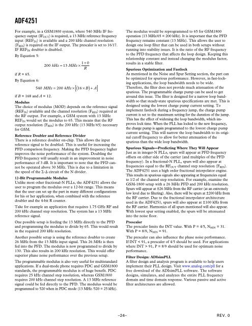
For example, in a GSM1800 system, where 540 MHz IF frequency<br />
output (IF OUT ) is required, a 13 MHz reference frequency<br />
input (REF IN ) is available and a 200 kHz channel resolution<br />
(F RES ) is required on the IF output. The prescaler is set to 16/17.<br />
IF REF IN doubler is disabled.<br />
By Equation 5:<br />
if R = 65.<br />
By Equation 6:<br />
if B = 168 and A = 12.<br />
1 0<br />
200 kHz = 13 MHz ¥ + R<br />
[( ) + A]<br />
540 MHz = 200 kHz ¥ 16 ¥ B<br />
Modulus<br />
The choice of modulus (MOD) depends on the reference signal<br />
(REF IN ) available and the channel resolution (F RES ) required at<br />
the RF output. For example, a GSM system with 13 MHz<br />
REF IN would set the modulus to 65. This means that the RF<br />
output resolution (F RES ) is the 200 kHz (13 MHz/65) necessary<br />
for GSM.<br />
Reference Doubler and Reference Divider<br />
There is a reference doubler on-chip. This allows the input<br />
reference signal to be doubled. This is useful for increasing the<br />
PFD comparison frequency. Making the PFD frequency higher<br />
improves the noise performance of the system. Doubling the<br />
PFD frequency will usually result in an improvement in noise<br />
performance of 3 dB. It is important to note that the PFD cannot<br />
be operated above 30 MHz. This is due to a limitation in<br />
the speed of the - circuit of the N divider.<br />
12-Bit Programmable Modulus<br />
Unlike most other fractional-N PLLs, the <strong>ADF4251</strong> allows the<br />
user to program the modulus over a 12-bit range. This means<br />
that the user can set up the part in many different configurations<br />
for his or her application, when combined with the reference<br />
doubler and the 4-bit R counter.<br />
Take for example an application that requires 1.75 GHz RF and<br />
200 kHz channel step resolution. The system has a 13 MHz<br />
reference signal.<br />
One possible setup is feeding the 13 MHz directly to the PFD<br />
and programming the modulus to divide by 65. This would result<br />
in the required 200 kHz resolution.<br />
Another possible setup is using the reference doubler to create<br />
26 MHz from the 13 MHz input signal. This 26 MHz is then<br />
fed into the PFD. The modulus is now programmed to divide by<br />
130. This also results in 200 kHz resolution. This would offer<br />
superior phase noise performance over the previous setup.<br />
The programmable modulus is also very useful for multistandard<br />
applications. If a dual-mode phone requires PDC and GSM1800<br />
standards, the programmable modulus is of huge benefit. PDC<br />
requires 25 kHz channel step resolution, whereas GSM1800<br />
requires 200 kHz channel step resolution. A 13 MHz reference<br />
signal could be fed directly to the PFD. The modulus would be<br />
programmed to 520 when in PDC mode (13 MHz /520 = 25 kHz).<br />
The modulus would be reprogrammed to 65 for GSM1800<br />
operation (13 MHz/65 = 200 kHz). It is important that the PFD<br />
frequency remains constant (13 MHz). This allows the user to<br />
design one loop filter that can be used in both setups without<br />
running into stability issues. It is the ratio of the RF frequency<br />
to the PFD frequency that affects the loop design. Keeping this<br />
relationship constant and instead changing the modulus factor,<br />
results in a stable filter.<br />
Spurious Optimization and Fastlock<br />
As mentioned in the Noise and Spur Setting section, the part can<br />
be optimized for spurious performance. However, in fast-locking<br />
applications, the loop bandwidth needs to be wide.<br />
Therefore, the filter does not provide much attenuation of the<br />
spurious. The programmable charge pump can be used to get<br />
around this issue. The filter is designed for a narrow loop bandwidth<br />
so that steady-state spurious specifications are met. This is<br />
designed using the lowest charge pump current setting. To<br />
implement fastlock during a frequency jump, the charge pump<br />
current is set to the maximum setting for the duration of the jump.<br />
This has the effect of widening the loop bandwidth, which improves<br />
lock time. When the PLL has locked to the new frequency,<br />
the charge pump is again programmed to the lowest charge pump<br />
current setting. This will narrow the loop bandwidth to its original<br />
cutoff frequency to allow for better attenuation of the<br />
spurious than the wide loop bandwidth.<br />
Spurious Signals—Predicting Where They Will Appear<br />
Just as in integer-N PLLs, spurs will appear at PFD frequency<br />
offsets on either side of the carrier (and multiples of the PFD<br />
frequency). In a fractional-N PLL, spurs will also appear at<br />
frequencies equal to the RF OUT channel step resolution (F RES ).<br />
The <strong>ADF4251</strong> uses a high order fractional interpolator engine.<br />
This results in spurious signals also appearing at frequencies equal<br />
to 1/2 of the channel step resolution. For example, examine the<br />
GSM-1800 setup with a 26 MHz PFD and 200 kHz resolution.<br />
Spurs will appear at ±26 MHz from the RF carrier (at an extremely<br />
low level due to filtering). Also, there will be spurs at ±200 kHz from<br />
the RF carrier. Due to the fractional interpolator architecture<br />
used in the <strong>ADF4251</strong>, spurs will also appear at ±100 kHz from<br />
the RF carrier. Harmonics of all spurs mentioned will also appear.<br />
With lowest spur setting enabled, the spurs will be attenuated<br />
into the noise floor.<br />
Prescaler<br />
The prescaler limits the INT value. With P = 4/5, N MIN = 31.<br />
With P = 8/9, N MIN = 91.<br />
The prescaler can also influence the phase noise performance.<br />
If INT < 91, a prescaler of 4/5 should be used. For applications<br />
where INT > 91, P = 8/9 should be used for optimum noise<br />
performance.<br />
Filter Design: ADIsimPLL<br />
A filter design and analysis program is available to help users<br />
implement their PLL design. Visit www.analog.com/pll for a<br />
free download of the ADIsimPLL software. The software<br />
designs, simulates, and analyzes the entire PLL frequency<br />
domain and time domain response. Various passive and active<br />
filter architectures are allowed.<br />
–24–<br />
REV. 0


