

UG-571 - Analog Devices
UG-571 - Analog Devices
UG-571 - Analog Devices

You also want an ePaper? Increase the reach of your titles
YUMPU automatically turns print PDFs into web optimized ePapers that Google loves.
<strong>UG</strong>-<strong>571</strong><br />
EVALUATION SOFTWARE FUNCTIONS<br />
The ADE7913 evaluation software allows access to all registers<br />
and features of the ADE7913. The menu options available are<br />
• Start the ADE7913s<br />
• Waveform Sampling<br />
• Synchronization<br />
• Emissions Management<br />
• Temperature Measurement<br />
• Read and Write Registers<br />
• Reset the ADE7913s<br />
• EXIT (stops LabView)<br />
The options provide access to all internal registers and allow<br />
the evaluation of the ADC performance. To access these<br />
functions, click the desired option in the MENU (see Figure 11).<br />
Clicking an option in the MENU displays a window where the<br />
specific function can be accessed. Each window includes an<br />
EXIT button used to return to the main window.<br />
Note that only one option from the MENU can be open at a<br />
time; click EXIT to return to the main window before choosing<br />
another option from the MENU.<br />
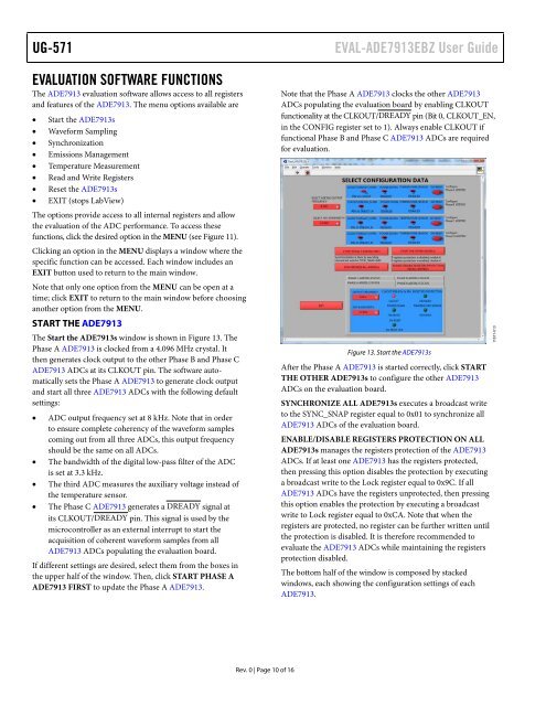
START THE ADE7913<br />
The Start the ADE7913s window is shown in Figure 13. The<br />
Phase A ADE7913 is clocked from a 4.096 MHz crystal. It<br />
then generates clock output to the other Phase B and Phase C<br />
ADE7913 ADCs at its CLKOUT pin. The software automatically<br />
sets the Phase A ADE7913 to generate clock output<br />
and start all three ADE7913 ADCs with the following default<br />
settings:<br />
• ADC output frequency set at 8 kHz. Note that in order<br />
to ensure complete coherency of the waveform samples<br />
coming out from all three ADCs, this output frequency<br />
should be the same on all ADCs.<br />
• The bandwidth of the digital low-pass filter of the ADC<br />
is set at 3.3 kHz.<br />
• The third ADC measures the auxiliary voltage instead of<br />
the temperature sensor.<br />
• The Phase C ADE7913 generates a DREADY signal at<br />
its CLKOUT/DREADY pin. This signal is used by the<br />
microcontroller as an external interrupt to start the<br />
acquisition of coherent waveform samples from all<br />
ADE7913 ADCs populating the evaluation board.<br />
If different settings are desired, select them from the boxes in<br />
the upper half of the window. Then, click START PHASE A<br />
ADE7913 FIRST to update the Phase A ADE7913.<br />
EVAL-ADE7913EBZ User Guide<br />
Note that the Phase A ADE7913 clocks the other ADE7913<br />
ADCs populating the evaluation board by enabling CLKOUT<br />
functionality at the CLKOUT/DREADY pin (Bit 0, CLKOUT_EN,<br />
in the CONFIG register set to 1). Always enable CLKOUT if<br />
functional Phase B and Phase C ADE7913 ADCs are required<br />
for evaluation.<br />
Figure 13. Start the ADE7913s<br />
After the Phase A ADE7913 is started correctly, click START<br />
THE OTHER ADE7913s to configure the other ADE7913<br />
ADCs on the evaluation board.<br />
SYNCHRONIZE ALL ADE7913s executes a broadcast write<br />
to the SYNC_SNAP register equal to 0x01 to synchronize all<br />
ADE7913 ADCs of the evaluation board.<br />
ENABLE/DISABLE REGISTERS PROTECTION ON ALL<br />
ADE7913s manages the registers protection of the ADE7913<br />
ADCs. If at least one ADE7913 has the registers protected,<br />
then pressing this option disables the protection by executing<br />
a broadcast write to the Lock register equal to 0x9C. If all<br />
ADE7913 ADCs have the registers unprotected, then pressing<br />
this option enables the protection by executing a broadcast<br />
write to Lock register equal to 0xCA. Note that when the<br />
registers are protected, no register can be further written until<br />
the protection is disabled. It is therefore recommended to<br />
evaluate the ADE7913 ADCs while maintaining the registers<br />
protection disabled.<br />
The bottom half of the window is composed by stacked<br />
windows, each showing the configuration settings of each<br />
ADE7913.<br />
11671-013<br />
Rev. 0 | Page 10 of 16


