

UG-571 - Analog Devices
UG-571 - Analog Devices
UG-571 - Analog Devices

Create successful ePaper yourself
Turn your PDF publications into a flip-book with our unique Google optimized e-Paper software.
EVAL-ADE7913EBZ User Guide<br />
<strong>UG</strong>-<strong>571</strong><br />
POWERING UP THE EVALUATION KIT BOARDS<br />
The interface board receives power via the USB cable that is<br />
connected to the PC. A 3.3 V regulator then powers the SDP<br />
board microcontroller and the ADE7913 ADCs populating the<br />
evaluation board. No additional power source is required for<br />
the ADE7913 evaluation kit boards.<br />
ANALOG INPUTS<br />
Current and voltage signals are connected at the test pins placed<br />
on the evaluation board. All analog input signals are filtered<br />
using the on-board antialiasing filters before the signals are<br />
connected to the ADE7913 ADCs. The components used on the<br />
board are the values recommended for use with the ADE7913.<br />
Current Sense Inputs (TP3 and TP2, TP8 and TP7, TP13<br />
and TP12 Test Pins)<br />
Every ADE7913 measures the voltage across a shunt at its IP<br />
and IM pins. Figure 4 shows the structure used for the Phase A<br />
current.<br />
The R8, R9, R20, and R21 are 0 Ω resistors that do not need<br />
to be implemented on a real meter board. The R15/C12 and<br />
R16/C15 RC networks are the antialiasing filters. The default<br />
corner frequency of these low-pass filters is 4.8 kHz (1 kΩ/<br />
33 nF). These filters can easily be adjusted by replacing the<br />
components on the evaluation board.<br />
The E1, E2, and E3 ferrite beads filter the high frequency noise<br />
that may be induced into the wires.<br />
The absolute maximum voltage on the IP and IM pins of the<br />
ADE7913 is ±2 V. The D3 and D6 diodes protect the IP and IM<br />
pins against voltages greater than ±1 V. The maximum signal level<br />
permissible at the IP pin of the ADE7913 is ±0.03125 V peak.<br />
The signal range should not exceed ±0.03125 V, with respect to<br />
AGND_ADC, for specified operation.<br />
The Phase A shunt is connected between the TP13 and TP12<br />
test pins.<br />
The other current channels (that is, Phase B and Phase C) have<br />
an identical input structure. The Phase B shunt is connected<br />
between the TP8 and TP7 test pins and the Phase C shunt is<br />
connected between TP3 and TP2.<br />
The shunt maximum value is a function of the maximum<br />
current to be measured on every phase:<br />
where:<br />
31.25×<br />
10<br />
R =<br />
2<br />
31.25×<br />
10<br />
2<br />
−3<br />
−3<br />
×<br />
1<br />
I FS<br />
is the rms value of the full-scale voltage accepted at the ADC<br />
input.<br />
IFS is the maximum current to be measured. It is called the fullscale<br />
current.<br />
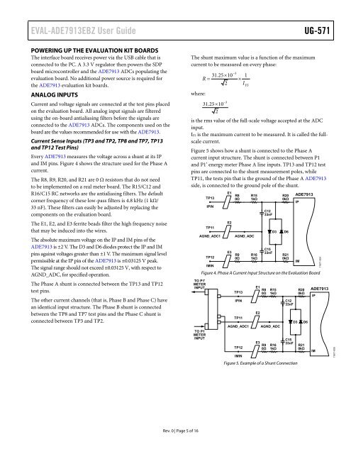
Figure 5 shows how a shunt is connected to the Phase A<br />
current input structure. The shunt is connected between P1<br />
and P1’ energy meter Phase A line inputs. TP13 and TP12 test<br />
pins are connected to the shunt measurement poles, while<br />
TP11, the tests pin that is the ground of the Phase A ADE7913<br />
side, is connected to the ground pole of the shunt.<br />
TP13<br />
IPIN<br />
TP11<br />
AGND_ADC1<br />
TO P1'<br />
METER<br />
INPUT<br />
TO P1<br />
METER<br />
INPUT<br />
TP12<br />
IMIN<br />
E1<br />
E2<br />
E3<br />
R8<br />
0Ω<br />
R15<br />
1kΩ<br />
AGND_ADC<br />
R9<br />
0Ω<br />
R16<br />
1kΩ<br />
R20<br />
0kΩ<br />
R21<br />
0kΩ<br />
Figure 4. Phase A Current Input Structure on the Evaluation Board<br />
TP13<br />
IPIN<br />
TP11<br />
AGND_ADC1<br />
TP12<br />
IMIN<br />
E1<br />
E2<br />
E3<br />
C12<br />
33nF<br />
C15<br />
33nF<br />
R8<br />
0Ω<br />
D3<br />
AGND_ADC<br />
R9<br />
0Ω<br />
R15<br />
1kΩ<br />
R16<br />
1kΩ<br />
D6<br />
C12<br />
33nF<br />
C15<br />
33nF<br />
Figure 5. Example of a Shunt Connection<br />
ADE7913<br />
IP<br />
D3<br />
IM<br />
R20<br />
0kΩ<br />
D6<br />
R21<br />
0kΩ<br />
11671-004<br />
ADE7913<br />
IP<br />
IM<br />
11671-005<br />
Rev. 0 | Page 5 of 16


