

Designing a Super-Heterodyne Multi-Channel ... - Analog Devices
Designing a Super-Heterodyne Multi-Channel ... - Analog Devices
Designing a Super-Heterodyne Multi-Channel ... - Analog Devices

You also want an ePaper? Increase the reach of your titles
YUMPU automatically turns print PDFs into web optimized ePapers that Google loves.
Abstract: This paper introduces an alternative receiver design<br />
that provides greater flexibility, cost effectiveness as well as<br />
providing a means for system upgrades and multi-leveled<br />
software. This receiver technology is known as multi-channel<br />
architecture and is possible through recent advances in analog<br />
converter technology, which now allow IF sampling which can<br />
greatly simplify receiver design. Additional advances in<br />
programmable digital integrated tuners simplify filter<br />
requirements, allowing their characteristics to be changed<br />
through software depending on channel bandwidth and data<br />
rates. Together the ADC and digital technology form a chipset<br />
that can eliminate many of the cumbersome stages of a<br />
traditional analog receiver with predictable and reliable<br />
performance and reduce the amount of hardware required for<br />
multi-channel receivers found in the typical BTS and WLL<br />
application.<br />
Using current state of the art ADCs such as the AD6600 and<br />
AD6640, IF sampling receivers are a reality. While each of<br />
these converters focus on different receiver applications, they<br />
both introduce true IF performance in data converters. The<br />
AD6600 is designed for single channel signal processing while<br />
the AD6640 is designed for true wide-band, multi-channel<br />
applications.<br />
RF stage<br />
receiver<br />
RF stage<br />
receiver<br />
RF stage<br />
receiver<br />
RF stage<br />
receiver<br />
IF stage<br />
receiver<br />
IF stage<br />
receiver<br />
IF stage<br />
receiver<br />
IF stage<br />
receiver<br />
While not the only use for such wide-band converters, they are<br />
used primarily used in multi-channel radios such as cellular,<br />
PCS and WLL base station receivers. But what level of<br />
performance can be achieved and what are the benefits and<br />
limitations of such receivers.<br />
Economics of <strong>Multi</strong>-Carrier Receivers<br />
Before an in depth discussion on performance expectations<br />
commences, a few economic comments are in order. In a<br />
traditional multi-channel receiver design, the receiver is<br />
duplicated once for each channel. This produces an overly<br />
redundant design. In addition to the duplication of receiver<br />
components, the labor to assemble and align these receivers is<br />
likewise duplicated.<br />
<strong>Designing</strong> a <strong>Super</strong>-<strong>Heterodyne</strong> <strong>Multi</strong>-<strong>Channel</strong> Digital Receiver<br />
Brad Brannon, <strong>Analog</strong> <strong>Devices</strong>, Inc.<br />
Greensboro, NC<br />
ADC-I<br />
ADC-Q<br />
ADC-I<br />
ADC-Q<br />
ADC-I<br />
ADC-Q<br />
ADC-I<br />
ADC-Q<br />
DSP<br />
<strong>Channel</strong><br />
1<br />
DSP<br />
<strong>Channel</strong><br />
2<br />
DSP<br />
<strong>Channel</strong><br />
3<br />
DSP<br />
<strong>Channel</strong><br />
n<br />
1<br />
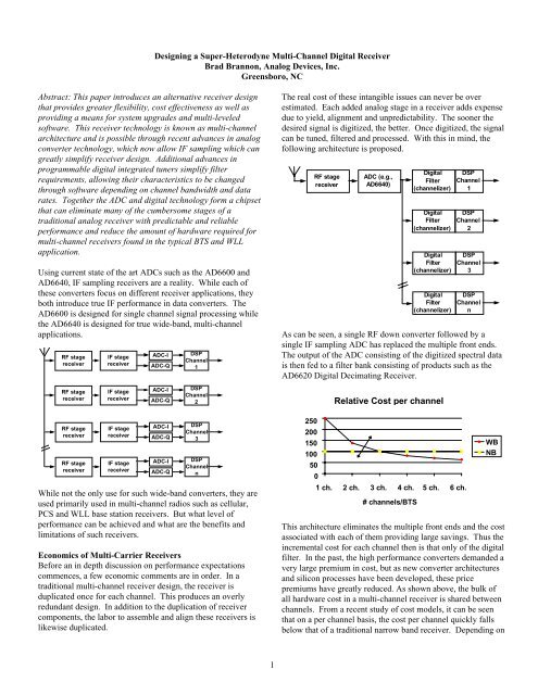
The real cost of these intangible issues can never be over<br />
estimated. Each added analog stage in a receiver adds expense<br />
due to yield, alignment and unpredictability. The sooner the<br />
desired signal is digitized, the better. Once digitized, the signal<br />
can be tuned, filtered and processed. With this in mind, the<br />
following architecture is proposed.<br />
RF stage<br />
receiver<br />
ADC (e.g.,<br />
AD6640)<br />
Digital<br />
Filter<br />
(channelizer)<br />
Digital<br />
Filter<br />
(channelizer)<br />
Digital<br />
Filter<br />
(channelizer)<br />
Digital<br />
Filter<br />
(channelizer)<br />
DSP<br />
<strong>Channel</strong><br />
1<br />
DSP<br />
<strong>Channel</strong><br />
2<br />
DSP<br />
<strong>Channel</strong><br />
3<br />
DSP<br />
<strong>Channel</strong><br />
n<br />
As can be seen, a single RF down converter followed by a<br />
single IF sampling ADC has replaced the multiple front ends.<br />
The output of the ADC consisting of the digitized spectral data<br />
is then fed to a filter bank consisting of products such as the<br />
AD6620 Digital Decimating Receiver.<br />
250<br />
200<br />
150<br />
100<br />
50<br />
0<br />
Relative Cost per channel<br />
1 ch. 2 ch. 3 ch. 4 ch. 5 ch. 6 ch.<br />
# channels/BTS<br />
WB<br />
NB<br />
This architecture eliminates the multiple front ends and the cost<br />
associated with each of them providing large savings. Thus the<br />
incremental cost for each channel then is that only of the digital<br />
filter. In the past, the high performance converters demanded a<br />
very large premium in cost, but as new converter architectures<br />
and silicon processes have been developed, these price<br />
premiums have greatly reduced. As shown above, the bulk of<br />
all hardware cost in a multi-channel receiver is shared between<br />
channels. From a recent study of cost models, it can be seen<br />
that on a per channel basis, the cost per channel quickly falls<br />
below that of a traditional narrow band receiver. Depending on
the assumptions made, the crossover point can occur with the<br />
first receive channel, especially when IF sampling is performed.<br />
Furthermore, as new channels are added to this receiver<br />
architecture, the cost per channel falls. That is, when the<br />
second channel is added, the receiver per channel cost only half<br />
of a typical base band-sampling receiver. These items in brief<br />
are the reasons why multi-channel receivers can provide a cost<br />
advantage. Although this has not been a detailed discussion, it<br />
should be evident why this is true.<br />
The Full <strong>Super</strong>-<strong>Heterodyne</strong> vs. IF Sampling Receiver<br />
Filter &<br />
LNA<br />
X<br />
Filter &<br />
LNA<br />
X<br />
LO LO LO<br />
Filter &<br />
LNA X Detector Process<br />
The block diagram of the super-het receiver is shown above.<br />
This triple conversion receiver is typical of many designs past<br />
and present. Sensitivity is gained by distributing the conversion<br />
gain between the antenna and the detector (often times a pair of<br />
base-band ADC and DSP). Distributing channel selection<br />
through the different stages derives selectivity. Quite often this<br />
is done with SAW filters or ceramic filters with specific<br />
characteristics determined by the air interface standard of<br />
interest. Additionally, most of the conversion gain occurs after<br />
the selectivity process begins so those amplifiers with lower<br />
IP3s can be used.<br />
Generally, the first local oscillator is variable and responsible<br />
for tuning while the second and third is fixed. The fixed local<br />
oscillators are usually simple in nature and implemented as<br />
crystal oscillators or synthesized with a low cost phased locked<br />
loop chip and VCO. The variable local oscillator however is<br />
another story. Some receiver architectures (such as GSM/DCS-<br />
1800/PCS-1900) require a frequency hoping that must slew and<br />
settle in very short order. Therefore, the tunable oscillator<br />
demands very close attention.<br />
Filter &<br />
LNA<br />
X<br />
LO<br />
Filter &<br />
LNA<br />
ADC AD6620<br />
To DSP<br />
The block diagram of the IF sampling receiver is shown above.<br />
This is actually a triple conversion receiver as well but perhaps<br />
not visibly so. The first down conversion is the obvious one.<br />
The output of the mixer is still an IF signal, possibly up to 90<br />
MHz or so. If the ADC is sampled at 40 MSPS, then the 90<br />
MHz signal is under-sampled and therefore aliased within the<br />
ADC. As long as the bandwidth of this signal(s) is less than 20<br />
MHz wide, the Nyquist principle is observed and the signal is<br />
aliased ( fSignal mod fSampleRate<br />
) to base-band without<br />
frequency distortion, only translation. Thus aliasing provides<br />
2<br />
the second down conversion. The final down-conversion is<br />
provided by the AD6620. This is a digital decimating receiver<br />
and designed to down convert the signal to based band.<br />
Therefore, it can be seen that this IF sampling receiver is<br />
actually still a triple conversion receiver, only the conversions<br />
take place through aliasing and numerically through the digital<br />
chips.<br />
One difference between these two receiver designs is that with<br />
the absence of IF stages, all of the conversion gain must take<br />
place prior to the ADC, either in the RF section or in the IF<br />
stages after the mixer. This requires that the components<br />
selected have a high IP3 since all selectivity is within the digital<br />
tuner. This is true because all signal paths, analog and mixed<br />
signal, must process the entire spectrum of signals.<br />
<strong>Multi</strong>-channel receivers offer several simplifications. First, the<br />
digital chip now replaces the variable local oscillator used for<br />
tuning. Thus the analog local oscillator is now fixed,<br />
simplifying the design greatly. Second, additional channels can<br />
easily be added by the addition of the digital tuner chips,<br />
adding greatly to the reliability of the system.<br />
Components Required<br />
Of course, to design and build such a receiver takes great<br />
consideration in component selection. Several key issues must<br />
be addressed. Of course, the issues of noise and intercept point<br />
are always of concern when it comes to receiver design, but<br />
issues of the data converter must also be discussed. This<br />
section will cover many of the components in the receiver.<br />
From our multi-channel IF sampling receiver, the first<br />
components of concern are the band select filter and LNA.<br />
These components are the same as those found in a single<br />
channel receiver. This is true because prior to the mixer in a<br />
single channel receiver, all signals are present. Therefore, no<br />
special points of concern exist with the LNA or filter. Of<br />
course, as with any front end, noise figure and IP3 are of great<br />
concern since overall noise filter is set by these components.
RF Filtering<br />
The RF filter is usually a helical filter. The purpose of this<br />
filter is to perform band selection; this is frequently called preselection.<br />
In a typical base station, this filter could consist of<br />
the bandwidth characteristics of the antenna, the RF trap or<br />
coupler (to keep Tx out of the Rx), and the broad band pass<br />
filter. As seen later, this filter should exhibit the lowest<br />
insertion loss possible, because receiver NF is directly (1 dB<br />
per dB) related to insertion loss at the front of the chain. High<br />
performance receivers would likely integrate a low loss micro<br />
strip filter directly on the PCB to minimize loss in this stage,<br />
especially 1800 and 1900 MHz applications. This filter ensures<br />
that following stages are not disrupted by any remaining out of<br />
band signals, including the base station transmit signals. The<br />
filters can be designed specifically to block the transmit side as<br />
in TOKO part numbers 6DFSC and 6DFSD.<br />
RF Amplifiers and Mixers<br />
RF gain stages are available in many forms, including discrete,<br />
monolithic and hybrid/MCM technologies. Many<br />
manufacturers offer RF front ends suitable for use in many low<br />
noise, high intercept applications. Many of these amplifiers<br />
offer 13 to 15 dB of gain with noise figures between 1.6 and 3.8<br />
dB with even better performance planned in the future. If ultralow<br />
noise figures are required, then discrete transistor<br />
amplifiers need be employed.<br />
While large RF gains improve overall noise figure they tend to<br />
worsen inter-modulation performance by increasing wide band<br />
signal levels to the mixer. Mixers tend to be the most difficult<br />
part of the receiver to satisfy.<br />
Low loss mixers (and hence low noise figure) should be used;<br />
however, they should have high intercept points. For example,<br />
a mixer with a +27 dBm LO drive level typically provides an<br />
input intercept point of +37 dBm. Thus, two signals at -43<br />
dBm would give 3rd order inter-modulation (IP3) products at<br />
about -200 dBm. However, if the intercept point were lowered<br />
to +17 dBm, these products would increase to -163 dBm. As<br />
signal levels are increased, inter-modulation performance will<br />
reduce rapidly. However, most air interface standards,<br />
including GSM and AMPS specification requires only -43 dBm<br />
two tone inter-modulation performance when receiving a<br />
reference sensitivity signal. Many mixers in this performance<br />
range are available. Since the RF mixer is so near the antenna<br />
with so little gain prior, noise is very important. When<br />
selecting mixers, it is often tempting to look at active mixers;<br />
however, quite often, active mixers have noise figures that are<br />
too large. Therefore, the popular choice tends to be the popular<br />
diode ring mixers. Since high linearity is required, these are<br />
usually the passive diode ring type mixers with high drive<br />
levels. These are available from a number of sources, insertion<br />
losses for the mixer is typically between 6 and 10 dB.<br />
In addition to the large LO drive levels for optimum<br />
performance, these LO signals must exhibit very low phase<br />
noise performance. The frequency domain process of the mixer<br />
3<br />
is convolution (the time domain process of the mixer is<br />
multiplication). As a result of mixing, phase noise from the LO<br />
causes energy from adjacent (and active) channels is integrated<br />
into the desired channel as an increased noise floor. This is<br />
called reciprocal mixing.<br />
IF Filtering and Amplification<br />
Once the signal has been mixed down to an IF that the ADC<br />
can handle, the signal must be filtered and then amplified. At<br />
this point, the signal must be gain to its full level because once<br />
digitized, the signal to noise ratio is fixed (except for process<br />
gains, see below). Unlike single channel filtering, a multicarrier<br />
radio must pass many channels at the same time.<br />
Therefore, the first implication is that the IF filter no longer<br />
determines channel bandwidth characteristics. The purpose of<br />
the IF filter is to prevent aliasing of unwanted signals by the<br />
ADC.<br />
There are two choices for IF filters. The most logical choice<br />
for IF filters is a SAW filter because of their relative low cost.<br />
However, since insertion loss is directly proportional to<br />
bandwidth, multi-channel filters are likely to incur a much<br />
higher loss than single channel filters. Where typical single<br />
channel losses are perhaps 5 dB, multi-channel SAWS may<br />
loose up to 25 dB, making post filtering gain a must. The<br />
second option for filtering is the traditional LC filter. While<br />
these tend to have phase some phase distortion and cost much<br />
more, they do have lower insertion losses, perhaps as little as 3<br />
dB.<br />
ADC Input Spectrum<br />
Band<br />
of<br />
Interest<br />
DC FS/2<br />
Signals aliased of off DC<br />
should be below desired<br />
signal level by the time<br />
it aliases here.<br />
Signals aliased of<br />
off FS/2 should be<br />
below desired signal<br />
level by the time it<br />
aliases here.<br />
Whether the signals alias off of DC or FS/2, filter skirts need be<br />
only as steep as that required preventing unwanted aliasing by
the time the filter skirts reach back to the band of interest as<br />
shown in the figure above. Thus higher sample rates provide<br />
ample opportunity to trade of filter transition bands and<br />
unwanted spurious placement.<br />
IF amplification is also a point of concern is a multi-channel<br />
receiver. Since a multi-channel receiver has no selectivity in<br />
the analog IF stage, the IF amp has to posses excellent IP3.<br />
This stage needs a lot of gain, low noise and very good<br />
linearity. If any of these fail to meet the mark, either sensitivity<br />
or adjacent channel rejection suffers. Again, looking back at<br />
the requirement for AMPS and GSM, two signals around –40’s<br />
dBm must co-exist without disruption to each other or other<br />
channels within the receiver.<br />
Since the gain from the antenna to the mixer is only minimal to<br />
prevent mixer overload, the level into the IF amplifier will be<br />
very close to that at the antenna port. If two signals at –43 dBm<br />
are placed at the antenna, they will be about that same level at<br />
the IF amp. Since typical receiver sensitivities are in the<br />
general area of about –110 dBm, the inter-modulation products<br />
of the IF amplifier must be better than –110 dBm referenced to<br />
the IF amplifier input. Thus a quick calculation places the input<br />
IP3 of the IF amplifier to be –4.5 dBm. Since amplifier IP3 is<br />
normally related to its output, this number must be increased by<br />
the gain of the stage. As will be seen later, IF gain<br />
requirements range from about 20 to 40 dB. Thus actual IP3<br />
requirements for the IF stage is up to +35 dBm!<br />
In addition to IP3, harmonic suppression can also be important<br />
if the IF is actually a base band application. Since this is a<br />
multi-channel receiver, broad ranges of frequencies are being<br />
processed. For example, a GSM receiver would digitize up to<br />
35 MHz, US cellular, up to 25 MHz or US PCS, 5 to 15 MHz.<br />
If these frequencies were translated to DC or near DC, then<br />
harmonics of these signals would fall back in band. For<br />
example, look at US PCS of 5 MHz. If the lowest frequency<br />
were translated to 1 MHz, the highest frequency of the band<br />
would be at 6 MHz. However, if a carrier were operational at<br />
the bottom of the band (1 MHz IF frequency), the second and<br />
third harmonic would fall at 2 and 3 MHz respectively, right in<br />
the middle of the band. These harmonics definitely can disrupt<br />
calls in a wide dynamic such as GSM or AMPS.<br />
Now consider the case where the bottom frequency of the band<br />
was translated to 5.1 MHz instead of 1 MHz. The upper<br />
frequency would align with 10.1 MHz. Now a quick look at the<br />
harmonics shows that the second harmonic of 5.1 MHz would<br />
fall at 10.2 MHz, outside the band of interest. The higher the<br />
IF frequency, the more spread out the harmonics and signals of<br />
interest become. In a practical sense, the IF frequency should<br />
be as high as the ADC could reasonably process.<br />
IF Amplification<br />
Op-amps are generally out of the question. First they are too<br />
noisy and second, they usually do not offer the spurious<br />
performance required for IF sampling. This leaves only the use<br />
4<br />
of IF gain blocks. Most of these devices are specified very well<br />
down to 5 to 10 MHz, which this application specifies.<br />
However, practical IF’s will often be around 70 MHz. IF gain<br />
blocks are useful in these applications as they offer IP3<br />
specifications as high as +40 dBm. However, when using IF<br />
gain blocks, care must be taken to remove the harmonics<br />
generated by these devices as they are different that those<br />
generated by the ADC. This should not pose a problem.<br />
IF Sampling ADC<br />
Recent advances in ADC technology have greatly improved the<br />
IF sampling capabilities of analog to digital converters. These<br />
improvements are allowing receiver architectures to emerge,<br />
primarily IF sampling designs such as those that are the focus<br />
of this article. Of those converters, the most current is the<br />
AD6640, a 12 bit 65 MSPS converter capable of base band<br />
performance up to 80 MHz.<br />
AIN<br />
AIN<br />
VREF<br />
ENCODE<br />
ENCODE<br />
Many of the issues that hold with the IF amplifiers hold true<br />
with the ADC as well. The important specifications are<br />
harmonic performance and two-tone inter-modulation (a<br />
version of IP3). Noise is also an issue, however, the usual<br />
design of the analog stage targets analog noise to be above the<br />
ADC noise so that it does not fully contribute to the receiver<br />
sensitivity.<br />
Digital Receiver Chip<br />
The purpose of the receiver chip is to tune in the desired carrier<br />
and then perform the channel selection of that carrier. Since the<br />
chip is fully programmable, the decimation rate and filter<br />
characteristics can be changed for each air interface as<br />
necessary. Since a typical system will require many receiver<br />
chips, it is possible for different air interface standards to be in<br />
operation at once. This is possible since each tuner chip can be<br />
programmed independent of the others. In this way, one chip<br />
can process AMPS and another TDMA or even CDMA.<br />
Real,<br />
Dual Real,<br />
or Complex<br />
Inputs<br />
AVCC<br />
A1 TH1<br />
TH2<br />
TH3 A2<br />
+2.4 V<br />
REFERENCE<br />
INTERNAL<br />
TIMING<br />
GND<br />
DVCC AD6640 FUNCTIONAL BLOCK DIAGRAM<br />
cos -sin<br />
Complex<br />
NCO<br />
ADC DAC<br />
I<br />
Q<br />
6<br />
CIC<br />
Filters<br />
External<br />
Sync<br />
Circuitry<br />
DIGITAL ERROR CORRECTION LOGIC<br />
I<br />
Q<br />
FIR<br />
Filter<br />
JTAG<br />
Port<br />
I<br />
Q<br />
ADC<br />
(MSB) (LSB)<br />
D11 D10 D9 D8 D7 D6 D5 D4 D3 D2 D1 D0<br />
Output<br />
Format<br />
μP<br />
or Serial<br />
Control<br />
7<br />
Serial or<br />
Parallel<br />
Outputs
The numerically controlled oscillator (NCO) provides spurious<br />
performance to better than -105 dBc. This ultra clean digital<br />
local oscillator is mixed with the digitized input through 18 bit<br />
multipliers. As shown in the spectral plot below of the NCO,<br />
spurious performance is hidden well in the 16-bit noise floor<br />
shown below.<br />
Other than programmable decimation rates, the response of the<br />
CIC filters are fixed. The FIR filters are fully programmable<br />
and the passband and stop-band characteristics can be<br />
programmed to nearly any unique specification.<br />
Inter-stage precision is maintained at 18 bits while individual<br />
stages use much higher precision to prevent artifacts due to<br />
truncation. Data out of the AD6620 can be delivered to the<br />
DSP through either a standard serial interface or through a<br />
parallel interface as a memory mapped address device. Data<br />
can be delivered in 16, 24 or 32 bit precision.<br />
Possible Receiver Designs<br />
The next section of this report summarizes the performance<br />
expectations for a multi-channel receiver as proposed here. For<br />
more detailed information of evaluating the performance of<br />
digital receiver designs, see the applications note titled ‘Basics<br />
of <strong>Designing</strong> a Digital Radio Receiver’. This application note<br />
outlines many of the considerations when designing a digital<br />
receiver and details how to compute receiver sensitivity as<br />
shown below. Throughout this section, the AD6640 is the<br />
proposed IF sample ADC converter. It should be noted that<br />
noise figure is omitted from this discussion. For a complete<br />
discussion on receiver design, including noise figure, see the<br />
applications note referenced above.<br />
# of <strong>Channel</strong>s<br />
to Break Even<br />
10<br />
GSM<br />
25<br />
8<br />
CDMA900 20<br />
PDC<br />
6<br />
D-AMPS<br />
AMPS<br />
CDMA1900<br />
DCS1800<br />
15<br />
4<br />
TACS<br />
NMT<br />
10<br />
2 PHS<br />
5<br />
0<br />
1993 1995 1997 1999<br />
0<br />
2001<br />
Relative Chipset<br />
Performance<br />
Improvements<br />
(dB)<br />
The chart above shows the progression of multi-channel multimode<br />
receivers. As seen, over the next few years, more and<br />
more air interface standards can be implemented with this<br />
5<br />
technology to reduce cost and greatly improve flexibility. In<br />
addition, this technology expands into third generation wireless<br />
communications as well. Potentially offering very flexible and<br />
fully programmable receiver design options.<br />
PHS/PACS<br />
PHS/PACS is a low mobility telephony system, initially<br />
deployed in Japan where it if fully deployed. Recently, many<br />
providers have begun to turn this into a wireless local loop<br />
standard for deployment around the world.<br />
The specifications below are for the PHS system. Referencing<br />
the digital receiver block diagram on page 3, the follow<br />
analysis is offered.<br />
Key Specification Level<br />
Sensitivity -91 dBm<br />
Maximum Blocker Level -41 dBm<br />
<strong>Channel</strong> Bandwidth 200 kHz<br />
Bit Rate 384 kSPS<br />
ADC Full Scale +4 dBm<br />
ADC SNR 68 dB<br />
From this table, the maximum allowable conversion gain can be<br />
computed.<br />
+4 - (-41) or 45 dB<br />
Allowing for 5 dB of headroom at the top gives 40 dB of<br />
conversion gain.<br />
The next question is what sample rate should be used. Since<br />
the AD6640 can sample up to 65 MSPS this forms our upper<br />
limit. As with all digital standards, the sample rate that is a<br />
multiple of the bit rate is the one to use. Since the incoming bit<br />
stream must be re-synchronized, we should use 4 samples per<br />
bit. This allows the DSP to determine which of the 4 samples is<br />
actually valid and toss the other three during equalization.<br />
Therefore, the effective bit rate out of the AD6620 must be 4<br />
time 384 kHz or 1.536 MHz. The first approximation can be<br />
found by dividing 65/1.536, which gives 42.317... Using the<br />
whole number only, 42 gives a usable sample rate of 42*1.536<br />
or 64.512 MSPS. 42 MSPS is also good because it can be<br />
easily factored by 2, 3, 6 and 7. A number that can be factored<br />
easily is required to distribute the decimation in the AD6620.<br />
After a complete filter analysis, the decimation rates used<br />
within the AD6620 are 3, 14 and 1. There are several that look<br />
good, but this one should minimize internal power dissipation.<br />
The next issue of concern is the processing gain. The actual<br />
filter bandwidth as determined from the AD6620 design<br />
software is 276kHz. Therefore, processing gain is:<br />
10 log(64.512/.276) or 23.7 dB.<br />
Finally the full-scale SNR with process gain is:
68 - 5(headroom) + 23.7(process gain) or 86.7 dB<br />
Since 10 dB of SNR is required for minimum detectability for<br />
most air interfaces, our signal may be reduced by 77 dB. If an<br />
input signal to the receiver of –41 dBm has an SNR of 87 dB,<br />
then the minimum detectable signal is:<br />
-41 dBm - 77 dB or -124 dBm<br />
The PHS/PACS spec for minimum signal level is -91 dBm;<br />
therefore, this wideband solution can work for PHS/PACS.<br />
CDMA<br />
CDMA air interfaces are becoming very popular for their<br />
security and flexibility. CDMA as IS-95 or other future<br />
standard offers many advances and features not found in other<br />
standards. When implemented using multi-channel techniques,<br />
multiple standards are possible. As such, one receiver can<br />
process AMPS and CDMA at the same time, possibly<br />
dynamically allocating spectrum as the demand and user<br />
profiles change.<br />
Key Specification Level<br />
Sensitivity -116 dBm<br />
Maximum Blocker Level -33 dBm<br />
<strong>Channel</strong> Bandwidth 1.25 MHz<br />
Bit Rate 1.2288 MCPS<br />
ADC Full Scale +4 dBm<br />
ADC SNR 68 dB<br />
The table above shows the critical operating specification of<br />
cellular CDMA (IS-95). From this table, the maximum<br />
allowable conversion gain can be computed.<br />
+4 - (-33) or 37 dB<br />
Again allowing for 5 dB of headroom at the top gives 32 dB of<br />
conversion gain.<br />
The next issue is how fast to run the sample clock. As with<br />
PHS, the AD6640 can sample up to 65 MSPS, however, in the<br />
end, we must make sure that our decimated data rate is at least<br />
2 samples per symbol so that timing/phase recovery can take<br />
place. Most CDMA application take 4 samples per symbol, so<br />
even still, interpolation of the output data must take place.<br />
Under these conditions, the decimation works out to be<br />
(65/(1.2288*2)) 26.44. Therefore, the nearest number that has<br />
good factors is 24. Therefore, the sample rate will be<br />
1.2288*2*24 or 58.9824 MHz.<br />
After carefully looking at the design, the decimation rates of 2,<br />
6 and 2 are selected. This decimation rate provides a total<br />
decimation of 24. This design is critical and may only<br />
marginally meet the specifications. CDMA requires a decent<br />
channel select filter to eliminate the image generated in the<br />
6<br />
digital tuners. CDMA may require extra computing power not<br />
available from a single AD6620. In cases such as this, several<br />
chips can be paralleled and the required poly-phase filter can be<br />
broken up and shared between the two filter chips. The input<br />
data to the AD6620 can be decimated between the two chips<br />
and the data out of the chips can be re-interleaved for signal<br />
processing as shown below.<br />
ADC<br />
/2<br />
AD6620 #1<br />
AD6620 #2<br />
Re-Interleave<br />
With these points given, the actual channel bandwidth for our<br />
examples is 1.344 MHz. Thus the process gain of our<br />
oversampling and filtering can be determined.<br />
10 log(65/1.344) or 16.8 dB.<br />
Computing SNR with process gain gives:<br />
68 - 5(headroom) + 17(process gain) or 80 dB.<br />
For a CDMA signal, a bank of filters matched to the PN<br />
signature sequences of each user, cause each user’s signal to be<br />
de-spread in frequency, thus affording a further gain in SNR.<br />
The spreading scheme described in IS-95 give rise to a<br />
processing gain (different from Process Gain, above) of 128.<br />
Assuming completely uncorrelated (or orthogonal) sequences,<br />
there is a de-spreading Gain of:<br />
10log(128) or 21.07 dB<br />
(1.2288 MHz / 9600 baud) is 128<br />
Since 10 dB of SNR is required for minimum detectability and<br />
our de-spreading gain is about 21 dB, then out signal can<br />
actually be hidden about 10 dB below the noise itself. Thus an<br />
actual SNR of –10 dB can recover our signal.<br />
If our signal for 80 dB SNR was -33 dBm, then the minimum<br />
detectable signal is:<br />
-33 dBm - 70 –20 dB or -123 dBm<br />
The minimum requirement for CDMA is -116 dBm.<br />
Considering that noise figure was ignored, a noise figure of<br />
only several dB would render this design useless. Therefore,<br />
the cellular CDMA example is a good candidate for a 14-bit<br />
converter. However a PCS CDMA implementation would<br />
possible make a good solution since the blocking specifications<br />
are somewhat reduced.<br />
DCS1800/PCS1900
GSM is deployed worldwide and is one of the most utilized<br />
standards around the world. GSM is now being deployed in<br />
many parts of the US as PCS1900. This version of GSM is an<br />
excellent target for a multi-channel receiver technology. These<br />
systems have limited bandwidths of 5 to 15 MHz making them<br />
well suited for band-pass sampling, placing harmonics out of<br />
band.<br />
Key Specification Level<br />
Sensitivity -101 dBm<br />
Maximum Blocker Level -25 dBm<br />
<strong>Channel</strong> Bandwidth 200 kHz<br />
Bit Rate 270.833 kBPS<br />
ADC Full Scale +4 dBm<br />
ADC SNR 68 dB<br />
The table above shows the critical specifications for GSM<br />
05.05 as implemented for DCS 1800. As before, this data can<br />
be used to calculate the maximum allowable conversion gain.<br />
+4 - (-25) or 29 dB<br />
Allowing for 4 dB of headroom at the top, this gives 25 dB of<br />
conversion gain.<br />
The AD6640 can sample up to 65 MSPS. In the end, we must<br />
make sure that our decimated data rate is 1 sample per symbol.<br />
One sample per symbol may be used for GSM since the coding<br />
scheme is differential. Therefore absolute phase is not as<br />
important as which way the vectors have rotated. Therefore,<br />
the spectral constellation does not have to have a specific<br />
alignment or timing, unlike CDMA or other standards. Since<br />
65 is divisible by 270.833 kBPS, the selected decimation is 240<br />
(65M/270.833K).<br />
Since the bandwidth of the GSM channel is 200 kHz, the digital<br />
filter used must provide the bandwidth and shaping required.<br />
At any rate the process gain can be computed based on this<br />
bandwidth.<br />
10 log(65/.252) or 24.1 dB.<br />
Finally, full-scale SNR with process gain is:<br />
68 - 4(headroom) + 24(process gain) or 88 dB.<br />
Since 10 dB of SNR is required for minimum detectability, our<br />
signal may be reduced by 78 dB. If our signal for 88 dB SNR<br />
was -25 dBm, then the minimum detectable signal is:<br />
-25 dBm - 78 dB or -103 dBm<br />
The minimum requirement for GSM1800/GSM1900 is -101<br />
dBm; therefore success can be achieved with the Wideband upbanded<br />
GSM with a little margin for noise figure. Finally, all<br />
of this assumes that dither is used to reduce the spurious<br />
performance into the noise floor.<br />
7<br />
AMPS<br />
AMPS cellular has one of the largest user bases of the air<br />
interfaces. It is likely that this standard will persist for many<br />
years to come. In order to reduce the cost of future system<br />
deployments and to facilitate multi-mode radios, AMPS is a<br />
very likely target for multi-channel radios. Along with AMPS,<br />
other standards such as NMT are prime candidates for this<br />
architecture.<br />
Key Specification Level<br />
Sensitivity -116 dBm<br />
Maximum Blocker Level -26 dBm<br />
<strong>Channel</strong> Bandwidth 30 kHz<br />
Deviation +/- 12.5 kHz<br />
ADC Full Scale +4 dBm<br />
ADC SNR 68 dB<br />
The maximum conversion gain is therefore computed as:<br />
+4 - (-26) or 30 dB<br />
Allowing for 5 dB of headroom at the top gives 25 dB of<br />
conversion gain.<br />
Since AMPS is not a digital standard, there is no key sample<br />
rate to work with. The main concern will be to sample at a rate<br />
that is at least twice the deviation of the signal. However, more<br />
importantly, if this is a multi-mode receiver, then the actual<br />
sample rate may be determined by the other standard.<br />
However, for the sake of this discussion, the full sample rate of<br />
65 MHz will be used. In the end, the data rate will be 4 times<br />
the deviation or 50 kHz. Thus this gives a decimation rate of<br />
1300 (65M/50k). With this large bandwidth, the FIR filter can<br />
utilize a maximum number of taps, giving an excellent filter<br />
shape rejecting adjacent channels well.<br />
Since our filter can be well formed, the bandwidth is 30 kHz.<br />
Therefore, processing gain is:<br />
10 log(65/.03) or 33.3 dB.<br />
With process gain at hand, the sensitivity can be calculated:<br />
68 - 5(headroom) + 33(process gain) or 96 dB.<br />
Since 10 dB of SNR is required for minimum detectability, the<br />
signal may be reduced by 86 dB. If our for 96 dB SNR was -26<br />
dBm, then the minimum detectable signal is:<br />
-26 dBm - 86 dB or -112 dBm<br />
The minimum requirement for AMPS is -116 dBm; therefore<br />
this fails to meet the requirements of the standard. There are<br />
two ways to get around this. The first is to demand a higher<br />
resolution ADC, such as 13 or 14 bits. The other solution is to<br />
reduce to -26 dBm blocker spec. This would allow more
conversion gain and thus better sensitivity. The AMPS spec<br />
does not specify this level; it is just a statistical measurement<br />
derived by signal measurements at our (ADI's) antenna site.<br />
Actually, the closest required specification is that of<br />
intermodulation for two signals at about -45 dBm. Therefore,<br />
the specification could be relaxed by about 20 dB at the<br />
expense of periodic performance degradation if a larger signal<br />
overdrives the input to the basestation. Therefore, by relaxing<br />
the spec to -36 dBm the minimum sensitivity (after an increase<br />
in conversion gain) is -123, more than enough to meet the<br />
specification.<br />
8


