

Bridge-Type Sensor Measurements are Enhanced ... - Analog Devices
Bridge-Type Sensor Measurements are Enhanced ... - Analog Devices
Bridge-Type Sensor Measurements are Enhanced ... - Analog Devices

Create successful ePaper yourself
Turn your PDF publications into a flip-book with our unique Google optimized e-Paper software.
<strong>Bridge</strong>-<strong>Type</strong> <strong>Sensor</strong> <strong>Measurements</strong> <strong>are</strong><br />
<strong>Enhanced</strong> by Autozeroed Instrumentation<br />
Amplifiers with Digitally Programmable<br />
Gain and Output Offset<br />
By Reza Moghimi [reza.moghimi@analog.com]<br />
Resistance-based bridge circuits <strong>are</strong> widely used to provide<br />
electrical outputs from sensors measuring physical variables, such<br />
as pressure and force. These outputs <strong>are</strong> usually small—and thus<br />
require amplification to bring them up to levels required by A/D<br />
converters in measurement-and-control systems. This article<br />
describes a versatile new IC instrumentation amplifier that has<br />
very low drift and many useful features, and discusses its role<br />
in solving problems of bridge instrumentation, using pressure<br />
measurement as an example.<br />
Pressure Sensing<br />
Figure 1 illustrates the functionality of a typical electrical<br />
output pressure instrument. Pressure is sensed by the motion of<br />
mechanical elements, such as diaphragms, Bourdon tubes, bellows,<br />
and capsules, all of which deflect when pressure is applied. This<br />
deflection causes a change in the resistances of a strain gage.<br />
PRESSURE<br />
SOURCE<br />
PRESSURE<br />
SENSOR<br />
(DIAPHRAGM)<br />
MECHANICAL<br />
OUTPUT<br />
STRAIN<br />
GAGE<br />
SIGNAL<br />
CONDITIONING<br />
ELECTRONICS<br />
Figure 1. Converting pressure to an electrical signal.<br />
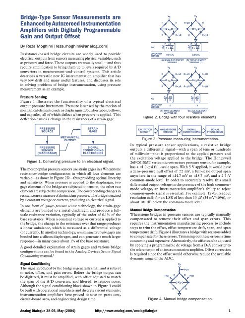
The most popular pressure sensors use strain gages in a Wheatstone<br />
resistance-bridge configuration in which all four elements <strong>are</strong><br />
variable—as shown in Figure 2D—thus providing optimal linearity<br />
and sensitivity. When pressure is applied to the diaphragm, two<br />
gage elements of the bridge <strong>are</strong> subjected to tension; the other two<br />
elements <strong>are</strong> subjected to compression. The corresponding changes in<br />
resistance <strong>are</strong> a measure of the incident pressure. The bridge is excited<br />
by a constant voltage or current, producing an electrical signal.<br />
In one form of gauge-pressure sensor technology, the strain-gage<br />
elements <strong>are</strong> bonded to a metal diaphragm and produce a fullscale<br />
resistance variation, typically of the order of 0.1% of the<br />
base resistance. When a constant voltage or current is applied to<br />
the bridge, the change in the resistance over that range produces<br />
a linear unbalance, which is measured as a differential voltage<br />
(or current). In another technology, semiconductor strain gages <strong>are</strong><br />
bonded into a silicon diaphragm, and can generate a much larger<br />
response—in many cases about 1% of the base resistance.<br />
A good detailed explanation of strain gages and various bridge<br />
configurations can be found in the <strong>Analog</strong> <strong>Devices</strong> <strong>Sensor</strong> Signal<br />
Conditioning manual. 1<br />
Signal Conditioning<br />
The signal produced by the bridge is generally small and is subject<br />
to noise, offset, and gain errors. Before the bridge output can<br />
be digitized, it must be amplified, with offset adjusted to match<br />
the span of the A/D converter, and filtered, to remove noise.<br />
Although the signal conditioning block shown in Figure 3 could<br />
be built with operational amplifiers and discrete circuit elements,<br />
instrumentation amplifiers have proved to save on parts cost,<br />
circuit-board <strong>are</strong>a, and engineering design time.<br />
<strong>Analog</strong> Dialogue 38-05, May (2004) http://www.analog.com/analogdialogue<br />
1<br />
V O:<br />
R<br />
R<br />
LINEARITY<br />
ERROR:<br />
V O:<br />
LINEARITY<br />
ERROR:<br />
V B<br />
4<br />
V B<br />
V O<br />
R<br />
R + R<br />
2<br />
R<br />
R+R<br />
R+R<br />
R<br />
V B<br />
2<br />
V B<br />
V O<br />
R<br />
R + R<br />
2<br />
0.5%/% 0.5%/%<br />
(A) SINGLE-ELEMENT<br />
VARYING<br />
R<br />
R<br />
V B<br />
2<br />
V B<br />
V O<br />
R<br />
R<br />
R–R<br />
R+R<br />
R<br />
R+R<br />
(B) TWO-ELEMENT<br />
VARYING (1)<br />
R+R<br />
R–R<br />
V B<br />
2<br />
V B<br />
V O<br />
R<br />
R<br />
0 0<br />
(C) TWO-ELEMENT<br />
VARYING (2)<br />
R–R<br />
R+R<br />
(D) ALL-ELEMENT<br />
VARYING<br />
Figure 2. <strong>Bridge</strong> with four resistive elements.<br />
EXCITATION<br />
CIRCUIT<br />
WHEATSTONE<br />
BRIDGE<br />
SIGNAL<br />
CONDITIONING<br />
SIGNAL<br />
PROCESSING<br />
Figure 3. Pressure measuring instrumentation.<br />
In typical pressure sensor applications, a resistive bridge<br />
outputs a differential signal—with a span of tens or hundreds<br />
of millivolts—that is proportional to the applied pressure and<br />
the excitation voltage applied to the bridge. The Honeywell<br />
26PC01SMT series microstructure pressure sensor, for example,<br />
has a 1.0-psi full-scale span. With 5 V applied, it would have<br />
a zero-pressure null offset of 2 mV, a full-scale output span<br />
anywhere in the range of 14.7 mV to 18.7 mV, and a 2.5-V<br />
common-mode level. In order to accurately resolve this small<br />
differential output voltage in the presence of the high commonmode<br />
voltage, an instrumentation amplifier’s ability to reject<br />
common-mode signal is essential. For example, 12-bit readout<br />
resolution calls for an LSB of less than 10 V (35 mV/4096), or<br />
about 101 dB below the common-mode level.<br />
Manual <strong>Bridge</strong> Compensation<br />
Wheatstone bridges in pressure sensors <strong>are</strong> typically manually<br />
compensated to remove their offset and span errors. This<br />
requires the instrumentation manufacturing process to include<br />
steps to trim the offset, offset temperature drift, span, and span<br />
temperature drift. Figure 4 illustrates a bridge with resistors added<br />
to compensate for these errors. Trimming out these errors is time<br />
consuming and expensive. Alternatively, the offset can be adjusted<br />
by applying a programmable dc voltage from a D/A converter to<br />
the reference pin of an instrumentation amplifier. Offset correction<br />
is required since the offset would otherwise reduce the available<br />
dynamic range of the ADC.<br />
POT<br />
R<br />
R<br />
V B<br />
V O<br />
POT<br />
R<br />
R<br />
POT<br />
Figure 4. Manual bridge compensation.
Gain uncertainties in pressure sensors make gain adjustment a<br />
requirement in most instrumentation amplifier-based systems.<br />
This was traditionally done by adding a trim potentiometer in<br />
series with the external gain resistor of the instrumentation<br />
amplifier. To achieve higher levels of performance over a wider<br />
temperature range, system designers turned to softw<strong>are</strong>-controlled<br />
gain compensation.<br />
Instrumentation Amplifier Errors<br />
Figure 5 shows some typical error sources that occur when a<br />
sensor is interfaced to a signal conditioning circuit. The bridge<br />
amplifier bias current flows through the output resistance of the<br />
bridge. Any unbalance in the resistance or bias current produces<br />
an offset error. This error, multiplied by the gain, appears at<br />
the output. In addition, the offset voltage and bias current <strong>are</strong><br />
functions of temperature. Other important errors to consider <strong>are</strong><br />
the amplifier’s gain accuracy, nonlinearity, and noise. A highperformance<br />
amplifier with low input offset voltage, bias current,<br />
offset-voltage TC, and bias-current TC is required for bridgemeasurement<br />
applications. 2<br />
V BIAS<br />
COPPER<br />
TRACES<br />
T1<br />
V OS<br />
+I BIAS<br />
KOVAR PINS –IBIAS 1<br />
2<br />
+IN<br />
–IN<br />
OUT<br />
T2<br />
THERMOCOUPLE VOLTAGES ≈ 35V/C (T1–T2)<br />
Figure 5. Amplifier error sources.<br />
The AD8555 to the Rescue<br />
Measurement system designs that use bridge circuits, such as<br />
pressure sensors, will benefit by the AD8555, a new zero-drift<br />
digitally programmable amplifier from <strong>Analog</strong> <strong>Devices</strong>. 3 Its<br />
instrumentation amplifier configuration employs three autozeroed<br />
amplifiers (A1, A2, A3), as shown in Figure 6.<br />
VNEG<br />
VPOS<br />
V DD<br />
A1<br />
VSS<br />
V DD<br />
A2<br />
VSS<br />
R1<br />
P1<br />
R3<br />
P2<br />
R2<br />
R4 P3 R6<br />
V DD<br />
A3<br />
VSS<br />
R5 P4 R7<br />
V DD<br />
DAC<br />
VSS<br />
VDAC<br />
VCLAMP<br />
RF<br />
FILT/<br />
DIGOUT<br />
V DD<br />
A5<br />
VSS<br />
V DD<br />
A4<br />
VSS<br />
Figure 6. Functional block diagram of the AD8555<br />
instrumentation amplifier.<br />
3<br />
VOUT<br />
To avoid loading the sensor’s bridge, the differential inputs feature<br />
high impedance and low bias current at both terminals (V POS<br />
and V NEG). Autozero techniques minimize offset and offset drift<br />
by continuously correcting for amplifier-generated dc errors.<br />
This results in a 10-V maximum input offset voltage over a<br />
temperature range of –40C to +125C, with maximum drift of<br />
just 65 nV/ C.<br />
Gain, ranging from 70 to 1280, is programmed in steps of<br />
less than 1 (with better than 0.4% resolution)—via a singlewire<br />
serial interface—by adjusting the gains of the two stages<br />
individually. In the DigiTrim ® process, the gain setting is locked<br />
in place by blowing polysilicon fuses. 4 The first-stage gain is<br />
trimmed from 4.00 to 6.40 in 128 steps by a 7-bit-code that<br />
adjusts both P1 and P2; and the second-stage gain is set from<br />
17.5 to 200 by an 8-step, 3-bit-code that adjusts P3 and P4. The<br />
adjustment values can be temporarily programmed, evaluated,<br />
and readjusted for optimum calibration accuracy—before the<br />
settings <strong>are</strong> permanently fixed.<br />
The AD8555 also has an 8-bit DAC- programmable offset, which<br />
can be used to compensate for offset errors in the input signal<br />
and/or add a fixed bias to the output signal. This bias is used,<br />
for example, to handle bipolar differential signals in a singlesupply<br />
environment. The output offset voltage may be set with a<br />
resolution of 0.39% of the voltage difference between the supply<br />
rails, (V DD–V SS).<br />
Vout = ( Gain) × ( Vdiff ) + Voffset<br />
2 <strong>Analog</strong> Dialogue 38-05, May (2004)<br />
and<br />
V<br />
where<br />
offset<br />
≈<br />
⎛<br />
⎝<br />
N<br />
− + 0. 5⎞<br />
× ( V − V ) + V<br />
256 ⎠<br />
DAC code<br />
DD SS SS<br />
Gain = (1 st -stage gain) (2 nd -stage gain)<br />
V diff is the differential input voltage to be measured<br />
N DAC-code is the numerical value of the DAC’s input code.<br />
Like the gain, the output offset can be temporarily programmed,<br />
evaluated, and readjusted; and then can be permanently set by<br />
blowing the fuse links.<br />
Single-supply operation has become an increasingly desirable<br />
characteristic of modern sensor amplifiers. Many of today’s data<br />
acquisition systems <strong>are</strong> powered from a single low voltage supply.<br />
The AD8555 operates from single-supply voltages from 2.7 V to<br />
5.5 V. The output of amplifier A4 swings to within 7 mV of either<br />
supply rail.<br />
Fault detection in the AD8555 amplifier protects against open,<br />
shorted, and floating inputs. Any of these conditions triggers a<br />
circuit that causes the output voltage to be clamped to the negative<br />
supply rail (V SS). Shorts and floating conditions <strong>are</strong> also detected<br />
on the V CLAMP input. Using an external capacitor, the AD8555<br />
can implement a low-pass filter to limit its dc-to-400-kHz output<br />
frequency range.<br />
The AD8555’s Role in <strong>Sensor</strong> <strong>Bridge</strong> Signal Conditioning<br />
Systems engineers would prefer that all pressure sensors with the<br />
same part number exhibit nearly identical performance. Typically,<br />
off-the-shelf sensors do not meet such requirements with adequate<br />
accuracy. One way to achieve consistency from sensor to sensor<br />
is extensive trimming during the manufacturing process. If the<br />
behavior of these sensors is repeatable over temperature, a better<br />
way may be to use this new generation of programmable amplifiers<br />
to provide compensation.<br />
The AD8555, with its zero-drift instrumentation amplifier, can<br />
provide amplification, gain setting and trim, offset setting and<br />
trim, and clamping—all established digitally. It can be used to<br />
compensate for offset and gain errors in bridge-type sensors, as<br />
well as providing an indication of sensor malfunction. It enables
adjustments using softw<strong>are</strong>, making compensation using trim<br />
potentiometers an outdated art in a manufacturing environment.<br />
In the many cases where sensors <strong>are</strong> used in harsh and crowded<br />
environments, measurements benefit from the wide temperature<br />
range and space-saving package size of the AD8555, which is<br />
housed in a 4-mm-by-4-mm lead-frame chip-scale package<br />
(LFCSP). Because the AD8555 is capable of driving very large<br />
capacitive loads, it can be placed close to the sensor and at a distance<br />
from the signal processing circuitry. Its high levels of programming<br />
flexibility and dc accuracy distinguish it from all other solutions.<br />
Application Example<br />
In a given batch of pressure sensors, sensor-to-sensor variations<br />
cause offset voltages of 20% of the sensor’s full-scale output.<br />
<strong>Sensor</strong>-to-sensor gain can vary by almost 2 to 1. The following<br />
example shows how we can use the AD8555 to compensate for the<br />
offset and gain variations, while maximizing the dynamic range<br />
of the signal provided to the A/D converter. Figure 7 shows the<br />
application circuit, including the bridge, AD8555, and AD7476<br />
A/D converter.<br />
26PC01SMT<br />
2.5k<br />
2.5k<br />
V DD<br />
2.5k<br />
2.5k<br />
2.5k<br />
2.5k<br />
1<br />
VDD VEE 8<br />
2<br />
FILTER VOUT 7<br />
3<br />
DATA VCLAMP 6<br />
4<br />
–IN<br />
+IN 5<br />
U14<br />
AD8555<br />
C8<br />
10nF<br />
SDATA<br />
V DD<br />
Figure 7. Pressure-sensing application example.<br />
V DD<br />
ADC<br />
AD7476<br />
<strong>Sensor</strong> characteristics<br />
The 26PC01SMT (surface-mount technology) pressure sensor<br />
is a Wheatstone bridge-based, printed circuit board-mountable<br />
device, which together with the AD8555, would appear to provide<br />
complete programmable pressure measurement and conditioning<br />
in a small footprint. Based on data sheet specifications at 10 V<br />
and 25C, these <strong>are</strong> the expected sensor characteristics with a<br />
5-V source:<br />
Gage, Vacuum Gage,<br />
Measurement <strong>Type</strong> Differential<br />
Pressure Range, psi 1.0<br />
Input Resistance Range, kilohms 5.5 to 11.5<br />
Output Resistance Range, kilohms 1.5 to 3.0<br />
Output Voltage Span, mV, 1 psi 14.7 min, 16.7 typ,<br />
18.7 max<br />
Span Shift Over Temperature, % 1.5 typ, 4.5 max<br />
Null Offset, mV –2 to +2<br />
Null Shift, mV, 25C to 0C; 1.0 max<br />
25C to 50C<br />
Linearity Error, % of Span 0.50 typ, 1.75 max<br />
Repeatability and Hysteresis Errors, % 0.20 typ<br />
Overpressure, lb/in 2 20 max<br />
Amplifier characteristics<br />
The signal conditioning circuitry also introduces errors which<br />
appear as an offset. The error contributions of the AD8555 <strong>are</strong><br />
listed in the following table.<br />
A IN<br />
Parameter Error PPM<br />
Input Offset Voltage (2 V + 2 mV/150) 150 458<br />
Input Offset Current 2500 ohm 200 pA 150 15<br />
Gain Error 0.5% 5000<br />
CMRR 100 dB 750<br />
Gain Nonlinearity (1) 50 ppm 50<br />
0.1–10 Hz 1/f Noise (2) 0.7 V p-p 150 21<br />
Total Unadjusted Error ~7 bits 6294<br />
Total Adjusted Error (1+2) ~14 bits 71<br />
Conditions: R bridge = 2500 ohm, Full scale = 16.7 mV, A V = 150, V OFF = 2.5 V,<br />
V OUT = 0 V to 5 V<br />
The table shows that the dominant error sources <strong>are</strong> static errors<br />
appearing at the input of the AD8555. These will be trimmed<br />
out along with the corresponding variations in the sensor. Errors<br />
caused by current noise, gain drift, and offset drift <strong>are</strong> minimal,<br />
and can be ignored. The remaining errors, which cannot be<br />
trimmed out, <strong>are</strong> noise and gain nonlinearity.<br />
Because noise places a limit on how accurately a sensor’s signal<br />
can be amplified, high resolution measurement of low-level signals<br />
requires a low noise, low drift amplifier. The AD8555 has a voltage<br />
noise density floor of 32 nV/÷Hz at 1 kHz. The noise from dc to<br />
10 Hz is 0.7 V peak-peak.<br />
The bridge, AD8555, and A/D converter <strong>are</strong> all excited by a +5-V<br />
supply. The full-scale output span of the bridge will be anywhere<br />
in the range of 14.7 mV to 18.7 mV. Its offset will be between<br />
–2 mV and +2 mV. Matching the 5-V full-scale input span of the<br />
A/D converter requires gain settings from 134 to 170. With the<br />
offset set to 2.5 V, the amplifier output will range from 0 V to 5 V<br />
as the pressure varies between –1 psi and +1 psi.<br />
First set the gain to 134—the minimum required by this sensor.<br />
With a 0-psi input, adjust the offset until the amplifier output is<br />
at 2.5 V. This compensates for the null offset of the sensor and<br />
the amplifier error terms. Apply a 1-psi input, and adjust the gain<br />
so that the amplifier output voltage is 5 V – 1 LSB. The output<br />
offset is a function of the gain, so the offset and gain adjustments<br />
must be done iteratively. As an alternative, the required gain can<br />
be calculated after the output span is measured. The offset is<br />
adjusted after the gain has been set, and thus only needs to be<br />
adjusted once.<br />
Conclusion<br />
The AD8555 simplifies the design of bridge measurement<br />
systems by integrating a zero-drift instrumentation amplifier<br />
with programmable gain, programmable output offset, fault<br />
detection, output clamping, and low-pass filtering, thus<br />
providing the complete signal conditioning path between a<br />
sensor and an A/D converter. An evaluation kit containing<br />
sample pieces and evaluation softw<strong>are</strong> and hardw<strong>are</strong>, is available<br />
from <strong>Analog</strong> <strong>Devices</strong>. b<br />
REFERENCES<br />
1 “<strong>Bridge</strong> Circuits”:, from Practical Design Techniques for <strong>Sensor</strong> Signal<br />
Conditioning, edited by Walt Kester, Norwood, MA: <strong>Analog</strong> <strong>Devices</strong>,<br />
Inc., 1999, Section 2. http://www.analog.com/<strong>Analog</strong>_Root/static/pdf/<br />
amplifiersLinear/training/<strong>Sensor</strong>_sect2.pdf<br />
2 <strong>Analog</strong> <strong>Bridge</strong> Wizard : A Tool for Design and Product Selection http:<br />
//www.analog.com/Wizard/bridge/bridgeUserEntry/<br />
3 AD8555 Description and Data sheet: http://www.analog.com. Enter<br />
in SEARCH box.<br />
4 Polysilicon fuses. One advantage of using polysilicon fuses is their reliable<br />
performance over temperature—a requirement in automotive applications,<br />
for example. Once the user is satisfied with the offset and gain settings, the<br />
trim circuit is locked out by blowing the master fuse to prevent any accidental<br />
re-trimming.<br />
<strong>Analog</strong> Dialogue 38-05, May (2004) 3


