Transceivermodule 1 TRX433-10A / TRX868-10A (Vers. 1.0E ...
Transceivermodule 1 TRX433-10A / TRX868-10A (Vers. 1.0E ...
Transceivermodule 1 TRX433-10A / TRX868-10A (Vers. 1.0E ...

Create successful ePaper yourself
Turn your PDF publications into a flip-book with our unique Google optimized e-Paper software.
<strong>Transceivermodule</strong> 1 <strong>TRX433</strong>-<strong>10A</strong> / <strong>TRX868</strong>-<strong>10A</strong> (<strong>Vers</strong>. <strong>1.0E</strong>)<br />
<strong>Vers</strong>ion list<br />
Datum <strong>Vers</strong>ion Beschreibung<br />
27.02.2007 <strong>1.0E</strong> German version 1.0 translated into english
<strong>Transceivermodule</strong> 2 <strong>TRX433</strong>-<strong>10A</strong> / <strong>TRX868</strong>-<strong>10A</strong> (<strong>Vers</strong>. <strong>1.0E</strong>)<br />
Table of contents<br />
<strong>Vers</strong>ion list .............................................................................................................................................. 1<br />
Table of contents .................................................................................................................................... 2<br />
Description.............................................................................................................................................. 3<br />
Features.................................................................................................................................................. 3<br />
Applications............................................................................................................................................. 3<br />
Family overview Radiotransceivers TRXnnn-10..................................................................................... 4<br />
Dimensions ............................................................................................................................................. 5<br />
Pin description ........................................................................................................................................ 5<br />
Linkcontrol mode..................................................................................................................................... 6<br />
RSSI (Received Signal Strenght indicator)............................................................................................. 6<br />
Powersupply ........................................................................................................................................... 6<br />
Datainterface with 5V Systems............................................................................................................... 6<br />
MCLR\ Reset .......................................................................................................................................... 6<br />
Timing and Handshake of communication ............................................................................................. 7<br />
Schematic with Hardwarehandshake .................................................................................................... 7<br />
Delay in data transmission Tdelay = t DATA + tRADIO ..................................................................................... 8<br />
Example: ................................................................................................................................................. 8<br />
Configuration setup................................................................................................................................. 9<br />
Technical Data <strong>TRX433</strong>-<strong>10A</strong> ................................................................................................................ 11<br />
Operating range.................................................................................................................................... 11<br />
Technical data <strong>TRX868</strong>-<strong>10A</strong>................................................................................................................. 12<br />
Simplified schematic TRXnnn-<strong>10A</strong> ....................................................................................................... 13<br />
Application example with <strong>TRX433</strong>-<strong>10A</strong> (Evalkit3) ............................................................................... 14<br />
Frequency table <strong>TRX433</strong>-<strong>10A</strong> .............................................................................................................. 15<br />
Frequency table <strong>TRX868</strong>-<strong>10A</strong> .............................................................................................................. 16<br />
Marking of the <strong>Transceivermodule</strong>: ...................................................................................................... 17<br />
CE declaration of conformity................................................................................................................. 18
<strong>Transceivermodule</strong> 3 <strong>TRX433</strong>-<strong>10A</strong> / <strong>TRX868</strong>-<strong>10A</strong> (<strong>Vers</strong>. <strong>1.0E</strong>)<br />
Description<br />
The transceiver modules <strong>TRX433</strong>-<strong>10A</strong> / <strong>TRX868</strong>-<strong>10A</strong> are narrowband intelligent RS232 serial radiomodems<br />
for the ISM frequency bands at 433MHz / 868MHz.To build a wireless radio link between two RS232 devices<br />
two transceivers TRXnnn-<strong>10A</strong> are needed. The radio protocol, data integrity check and handshake are<br />
managed by the intelligent module itself. With an initial configuration the trasnsceiver can be put to the users<br />
need. A link control function with a RSSI voltage output can be used to test the quality of the radio link.<br />
With this transceivers you can realize excellent operating ranges.<br />
Features<br />
• easy configuration of communication parameters like frequency, baudrate, handshake and RF-mode<br />
through simple RS232 commands<br />
• integrated link control function<br />
• narrowband radio modem with 139 / 159 frequency channels in a 12.5kHz grid<br />
• RF-mode selects max. operating range (2km) max. speed (19kbits/s) or standard setting<br />
• compact size, small weight<br />
• status LED<br />
• three pincompatible versions A, B, C for different application types available.<br />
functionality (software) can be customized for special demands<br />
Applications<br />
• bidirectional RS232 data communication<br />
• fully replaces RS232 cables and provides galvanic isolation<br />
• wirless terminals, printers, displays<br />
• PC-PC data communication with terminalprogram (Hyperterminal)<br />
• with Evalkit3 range tests can be made<br />
We recommend the Evaluationkit 3 as a comfortable starting point for the first-time user of the TRXnnn-10<br />
and also as a reference design. With this kit you can realize within a few minutes a bidirectional serial PC-PC<br />
or PC to printer communication. You can also evaluate the operating distance in the field, without using any<br />
PC.
<strong>Transceivermodule</strong> 4 <strong>TRX433</strong>-<strong>10A</strong> / <strong>TRX868</strong>-<strong>10A</strong> (<strong>Vers</strong>. <strong>1.0E</strong>)<br />
Family overview Radiotransceivers TRXnnn-10<br />
The Radiotransceivers of the <strong>TRX433</strong> and <strong>TRX868</strong> family are offered in three different versions, which are<br />
different in software and / or in hardware.<br />
Today the three versions A, B and C exists, with the following main differences:<br />
<strong>Vers</strong>ion A <strong>Vers</strong>ion B <strong>Vers</strong>ion C<br />
Data interface RS232 any, transparent RS232<br />
Configuration<br />
through RS232<br />
Sleep, Powerdown,<br />
Wakeup features<br />
Only most important<br />
parameters, only<br />
possible at powerup<br />
Delay TX-RX 1 t DATA + tRADIO ,<br />
see timing diagram<br />
Comprehensive command<br />
set, configurable anytime,<br />
also while operating<br />
no yes yes<br />
6 t BIT-RADIO<br />
Jitter +- 1/8 t BIT-RADIO<br />
Comprehensive command<br />
set, configurable anytime,<br />
also while operating<br />
8 t BIT_DATA + 50 t BIT_RADIO<br />
Error checking CRC16 none with / without CRC16<br />
Retransmit after<br />
receive error<br />
Yes, until receiver<br />
acknowledges correctly<br />
no no<br />
Buffersize TX 2 x 31 Bytes Ringbuffer, 63 Bytes 2<br />
Buffersize RX 1 x 31 Bytes, Ringbuffer Ringbuffer, 63 Bytes 2<br />
data handshake RTS-CTS, XON-XOFF RTS-CTS<br />
The three versions are covering the different needs of most applications as follow:<br />
<strong>Vers</strong>ion A is meant for simple applications as cable replacement e.g. between PC and peripheral devices, if<br />
the time delay of the radio link doesn’t play any role. The Transceiver himself checks for errors in the<br />
reception, sends an acknowledge back to the transmitter, which repeats the message in case of an error.<br />
The data are transmitted over radio after the buffer is full or if during a time of 3ms no further data are<br />
received. The Evalkit3 with the <strong>Vers</strong>ion A of the Transceiver is ideally suited to test the radio range.<br />
<strong>Vers</strong>ion B is used, if maximum transparency and control of the radio link is necessary or wished. There’s<br />
absolutely no coding or error check done. The input signal of the transmitter will be transmitted to the<br />
receiver transparently and with a minimal delay, so the receiver outputs a 1:1 copy of the transmitter input<br />
signal. This version nearly emulates a direct wire connection and gives maximum compatibility to any coding<br />
scheme and radio module of other manufacturers.<br />
<strong>Vers</strong>ion C with a transparent byte mode is used, if short response times are needed for RS232 data<br />
communication, and if you need full and easy control over many parameters of the communication. The<br />
serial bytes input at the transmitter side are sent almost immediately, so the data will be output at the<br />
receiver side only a few milliseconds later. If Error-checking is activated, the receiver outputs data only after<br />
they are checked and ok. Without internal errorchecking, the user has to implement this task itself within the<br />
application. <strong>Vers</strong>ion C works well with protocols like X, Y, Z-modem because of the minimal timedelay.<br />
1 tBIT_DATA : time of 1 Bit of the RS232 input data at the transmitter side<br />
t BIT_RADIO : time of 1 Bit of the selected radio datarate<br />
2<br />
if the radio datarate is fast enough with respect to the RS232 baudrate, a continuous dataflow will result<br />
without interruption by the Handshake.
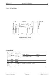
<strong>Transceivermodule</strong> 5 <strong>TRX433</strong>-<strong>10A</strong> / <strong>TRX868</strong>-<strong>10A</strong> (<strong>Vers</strong>. <strong>1.0E</strong>)<br />
Dimensions<br />
0.5mm 24.5mm<br />
Pin description<br />
40.0mm<br />
<strong>TRX433</strong>-10<br />
<strong>TRX868</strong>-10<br />
front view<br />
14 13 12 11 10 9 8 7 6<br />
2 1<br />
2.54mm 10.16mm 2.54mm<br />
Leadframe: pins 0.5 x 0.2mm<br />
Pin Name I/O Description level condition<br />
4.5mm<br />
1 RF I/O RF- in/out for lambda / 4 antenna (~ 50 Ω) 0 V DC-path to GND<br />
2 GND RF Signal Ground<br />
6 V_P O Programming voltage (do not connect) VCC<br />
7 MCLR\ I Reset input, active low. 3 VCC Normal operation<br />
8 RSSI O Received Signal Strength Indicator (analog) 29dB/V uncalibrated<br />
9<br />
RTS<br />
CFG<br />
TEST<br />
O<br />
I<br />
I<br />
Request To Send. 4<br />
enters config.mode, if high during powerup. 4<br />
enters linkcontrol mode, if high after powerup<br />
0 V<br />
VCC<br />
0 V<br />
0 V<br />
Normal operation<br />
RX-Buffer full<br />
Normal operation<br />
Normal operation<br />
10 TxD O Transmit Data (digital out) VCC Stop bit or no data<br />
11 RxD<br />
LINK\<br />
I<br />
O<br />
Receive Data (digital in)<br />
shows successful link, if TEST high<br />
12 CTS I Clear To Send (digital in)<br />
13 V+ Positive supply voltage. 5<br />
14 GND Ground<br />
VCC<br />
0 V<br />
0 V<br />
VCC<br />
Stop bit or no data<br />
Successful link<br />
Normal operation<br />
TRX stops transm.<br />
3<br />
connect an external reset controller, if supply voltage is not always within specified limits or if voltage<br />
ramp is slower than 50ms from 0V to 3.5V.<br />
4<br />
connect a pulldown resistor of 100k to GND for normal operation<br />
5<br />
VCC = 3.3V is the internal regulated supply voltage (standard version with 3.3V regulator)<br />
VCC = V+ in case of no internal voltage regulator See simplified schematic of Transceiver
<strong>Transceivermodule</strong> 6 <strong>TRX433</strong>-<strong>10A</strong> / <strong>TRX868</strong>-<strong>10A</strong> (<strong>Vers</strong>. <strong>1.0E</strong>)<br />
Linkcontrol mode<br />
Pin 9 (TEST) of the <strong>Transceivermodule</strong> has two functions, one for the flow-control (handshake) and the<br />
second function is the link-control. The link-control signals a valid, bidirectional link to a second partner-<br />
<strong>Transceivermodule</strong>.<br />
If TEST is set high through a resistor, the status of the radio-link to the partnermodem is output on the signal<br />
LINK\.<br />
LINK\ low means radio communication is OK<br />
LINK\ high means no radio communication<br />
Because TEST as well as LINK\ are double used and depending on the application are used as an input or<br />
an output, please take care not to connect two outputs without any current-limitation resistor together and<br />
also prevent the situation of an open input.<br />
As an example we refer to the application schematic of the Evalkit3, where the link-control is realized with a<br />
push-button and a LED.<br />
Important notice:<br />
Pin 9 must be connected with a Pulldown resistor (e.g. 100 k) to GND, so that the configuration mode cannot<br />
be activated unintentional during powerup of the <strong>Transceivermodule</strong>.<br />
If during powerup pin 9 is already high, the configuration mode is activated.<br />
RSSI (Received Signal Strenght indicator)<br />
The voltage at pin 8 (RSSI) is directly proportional to the receiving field intensity. The higher this voltage is<br />
the higher is also the receiving field intensity. The scaling is approx. 29dB/V, the offset or zero point is not<br />
calibrated and depends on the RF-mode.<br />
Powersupply<br />
The Radiotransceiver needs a clean supply voltage of min. 3.5V with a ripple of < 10mVpp.<br />
The power amplifier of the radio transmitter is directly connected to the input supply voltage, the rf-transmitter<br />
power therefore depends a little on the input supply voltage.<br />
If the supply of the <strong>Transceivermodule</strong> is switched, the voltage must always sink to 0V, before switching on<br />
the supply again. The supply voltage must rise within max. 50ms from 0V to 3.5V, so that the integrated<br />
microcontroller starts correctly. The voltage may never fall below 3.3 V, not even for a short time.<br />
If this cannot be ensured, the supply voltage must be supervised by a Voltagedetector, which ties the MCLR\<br />
input low as soon as the voltage drops below approx. 3.3V. See also application example with Evalkit3.<br />
Datainterface with 5V Systems<br />
The logic levels of the <strong>Transceivermodule</strong> are 3.3 Volt, according to the int. voltage regulator. The<br />
Transceiver can work directly at 5Volt systems, however during the high level of the 5V system an additional<br />
small current flows over the internal series resistors into the Transceiver. The input high-levels of the 5V<br />
system must be compatible to the 3.3V logic. See also simplified schematic of the Transceiver<br />
MCLR\ Reset<br />
The microcontroller of the <strong>Transceivermodule</strong> hasn’t got an internal Reset-detector, so the reset pin is<br />
externally accessible. We recommend an external Voltage detector with a trip voltage of > 3.3Volt (for<br />
standard TRX with 3.3V internal voltage regulator). If no such detector is used, please read the datasheet of<br />
the Microchip 16LF648A and ensure that the supply voltage conditions for powerup, brownout etc. can be<br />
met. The most problematic situation exists, when the supply voltage drops below 3.5 Volt and then again<br />
rises to normal condition, without going to nearly zero Volt.<br />
Anyway, with an external voltage detector, these problems are solved.<br />
If the conditions described under paragraph Powersupply are all met, the external reset-controller or voltage<br />
detector can be omitted.
<strong>Transceivermodule</strong> 7 <strong>TRX433</strong>-<strong>10A</strong> / <strong>TRX868</strong>-<strong>10A</strong> (<strong>Vers</strong>. <strong>1.0E</strong>)<br />
Timing and Handshake of communication<br />
The following example shows an unidirectional data communication of DEVICE1 to DEVICE2 with hardware<br />
handshake. If the data source sends more data than the Transceiver can buffer (>31 byte), a handshake is<br />
absolutely necessary, so that no data are lost. The databuffer of DEVICE1 is sent, as soon as it is full or if<br />
during the time of 3ms no more data arrive. The data communication is symmetrical and identical in both<br />
directions.<br />
The Transceiver data are double buffered (2x31 bytes) at the transmitter side. The first Buffer takes up the<br />
data from RS232 and passes them to the transmitter buffer before the start of the transmission. There the<br />
data are kept until an answer (ACK) from the receiver confirms the successful radio transmission. Meanwhile<br />
the first Buffer receives already new data from the RS232. The transmitter repeats the radio transmission of<br />
the data in the transmitter buffer as long as he receives a successful answer (ACK) from DEVICE2. Then,<br />
the next data block from the RS232 Buffer will be shifted into the transmitter buffer.<br />
The data buffer at the receiver-side is designed as a ringbuffer. This allows to receive new data over radio as<br />
soon as the buffer is going to be emptied into the RS232 interface.<br />
RXD_1<br />
RTS_1<br />
Radio1 state<br />
TXD_1<br />
CTS_1<br />
TXD_2<br />
CTS_2<br />
Radio 2 state<br />
RXD_2<br />
RTS_2<br />
1 2 3 4 5 6 7 8 9 10 11 12 13 14 15 16 17 18 19 20 21 22 23 24 25 26 27 28 29 30 31<br />
Transceiver DEVICE 1 sends 70 Bytes<br />
receive<br />
31 Databytes<br />
Transceiver DEVICE 2<br />
receive<br />
31 Databytes<br />
Tdata Tradio<br />
transmit<br />
Tdelay<br />
Schematic with Hardwarehandshake<br />
PC, Terminal<br />
RTS<br />
TXD<br />
RXD<br />
CTS<br />
TRX, DEVICE 1<br />
CTS<br />
RXD<br />
TXD<br />
RTS<br />
RX Buffer1 full<br />
receive<br />
31 Bytes 70 Bytes from DEVICE 1 31 Bytes 8 Bytes<br />
ACK<br />
acknowledge<br />
RADIO<br />
Link<br />
8 Databytes<br />
transmit<br />
receive<br />
TRX, DEVICE 2<br />
CTS<br />
RXD<br />
TXD<br />
RTS<br />
receive<br />
ACK<br />
acknowledge<br />
transmit<br />
receive<br />
ACK<br />
acknowledge<br />
PC, Terminal<br />
RTS<br />
TXD<br />
RXD<br />
CTS
<strong>Transceivermodule</strong> 8 <strong>TRX433</strong>-<strong>10A</strong> / <strong>TRX868</strong>-<strong>10A</strong> (<strong>Vers</strong>. <strong>1.0E</strong>)<br />
RXD_1<br />
RTS_1<br />
Radio1 state<br />
TXD_1<br />
CTS_1<br />
TXD_2<br />
CTS_2<br />
Radio 2 state<br />
RXD_2<br />
RTS_2<br />
1 2 3 4 5 6 7 8 9 10 11 12 13 14 15 16 17 18 19 20 21 22 23<br />
Transceiver DEVICE 1 sends 8 Bytes<br />
receive<br />
8 Databytes<br />
Transceiver DEVICE 2<br />
receive<br />
Tdata<br />
3ms<br />
Tradio<br />
Tdelay<br />
Delay in data transmission Tdelay = t DATA + tRADIO<br />
tdata<br />
n Bytes • 10 bits<br />
=<br />
baudrate<br />
transmit<br />
(n + 8)<br />
Bytes • 8bits<br />
tradio =<br />
RF_bitrate<br />
receive<br />
5 Bytes 8 Bytes from DEVICE 1 3 Bytes<br />
Tack<br />
ACK<br />
acknowledge<br />
receive<br />
Example:<br />
RS232 Baudrate = 9600 bits/s, RF-bitrate = 4800 bits/s, 31 databytes:<br />
Tdelay = tDATA + tRADIO = 31 x 10 / 9600 + (31+8) x 8 / 4800 = 32.3ms + 65.00ms = 97.30ms<br />
8 Bytes • 8 bits<br />
=<br />
RF_bitrate<br />
RS232 Baudrate = 57600 bits/s, RF-bitrate = 19200 bits/s, 10 databytes:<br />
Tdelay = t DATA + 3ms+ tRADIO = 10 x 10 / 57600 + 3ms + 18 x 8 / 19200 = 1.74ms + 3ms + 7.5ms = 12.2ms<br />
tack
<strong>Transceivermodule</strong> 9 <strong>TRX433</strong>-<strong>10A</strong> / <strong>TRX868</strong>-<strong>10A</strong> (<strong>Vers</strong>. <strong>1.0E</strong>)<br />
Configuration setup<br />
If the signal CFG (Pin9) is held high during the powerup of the Transceiver, the module enters into the<br />
configuration mode (this would also happen if the yellow button was pushed on Evalkit3 while powerup).<br />
The configuration works with a fixed baudrate of 19.2kbaud and the following parameters:<br />
Configuration: - Baudrate: 19.2 kbaud<br />
- Databits: 8 Bit’s<br />
- Parity: none<br />
- Stop-Bit: 1<br />
- Handshake none<br />
The most convenient way to configure the Transceiver is to use the Evalkit3 together with Hyperterminal,<br />
where you will see the following screen.<br />
Screen output in Hyperterminal after start of configuration:<br />
If you use the Evalkit3 for configuration, you can switch the supply of the Transceiver by means of the<br />
„connect“ and „disconnect“ button of Hyperterminal (this are the buttons with the telefon symbol).<br />
Now you can setup the following 4 Parameters (Input numbers, ENTER, ESC)<br />
frequency: at 433MHz- band: possible frequencies: 1-139 (in 12.5kHz-steps)<br />
001 = 433.0625 MHz (also input the leading zeros!)<br />
070 = 433.9250 MHz<br />
139 = 434.7875 MHz<br />
At 868MHz- band: possible frequencies: 1-159 (in 12.5kHz-steps)<br />
001 = 868.0125 MHz (also input the leading zeros!)<br />
080 = 869.0000 MHz<br />
159 = 869.9875 MHz<br />
baudrate: Baudrate for RS-232 Interface:<br />
1 = 1.2 kbaud<br />
2 = 2.4 kbaud<br />
3 = 4.8 kbaud<br />
4 = 9.6 kbaud<br />
5 = 19.2 kbaud<br />
6 = 38.4 kbaud<br />
7 = 57.6 kbaud
<strong>Transceivermodule</strong> 10 <strong>TRX433</strong>-<strong>10A</strong> / <strong>TRX868</strong>-<strong>10A</strong> (<strong>Vers</strong>. <strong>1.0E</strong>)<br />
rf-mode: Setup for radio transmission:<br />
1 = 19.2 kbit radio datarate, 100kHz channel grid (Maximum data speed)<br />
2 = 4.8 kbit radio datarate, 25kHz channel grid (Standard setup)<br />
3 = 1.2 kbit radio datarate, 12.5kHz channel grid (Maximum sensitivity)<br />
handshake: Flow control: (for reliable communication flow control should always be activated)<br />
1 = no flow control<br />
2 = Hardware (RTS/CTS)<br />
3 = Software (XON/XOFF)<br />
The configuration mode can be terminated with the ESC-Key or it will terminate automatically after 1 Minute<br />
of no data activity.<br />
If you want a parameter not to change, hit the Enter-Key without any number input.<br />
The configuration is saved into the EEPROM of the <strong>Transceivermodule</strong> and will remain there permanently.<br />
Notice:<br />
• The configuration must be done always with 19.2kbaud, even if you configured another baudrate<br />
• The signal RTS/CFG (Pin 9) must be tied to a logic low level by a pulldown resistor during normal<br />
operation, in order not to activate the configuration mode during powerup.<br />
• Always input the numbers with three figures, including the leading zeros<br />
• With the standard 868MHz Transceiver, only use rf-mode = 3, if the temperature range in use is<br />
between 5°C and 40°C.
<strong>Transceivermodule</strong> 11 <strong>TRX433</strong>-<strong>10A</strong> / <strong>TRX868</strong>-<strong>10A</strong> (<strong>Vers</strong>. <strong>1.0E</strong>)<br />
Technical Data <strong>TRX433</strong>-<strong>10A</strong><br />
Frequency range 433.0625 .... 434.7875 MHz (12.5 kHz steps)<br />
Communication settings:<br />
RFmode = 3<br />
RFmode = 2<br />
RFmode = 1<br />
Frequency accuracy<br />
Transmitter power<br />
Receiver sensitivity<br />
(50 Ohm / BER = 1E-3)<br />
Chann. steps IF-bandwith Radio -datarate FM-Deviation<br />
12.5 kHz<br />
25.0 kHz<br />
100 kHz<br />
9.6 kHz<br />
19.2 kHz<br />
51.2 kHz<br />
1.2 kbit/s Manchester<br />
4.8 kbit/s NRZ<br />
19.2 kbit/s NRZ<br />
+- 5ppm standard (Temp. -10°C ... +60°C)<br />
+- 2ppm optional (Temp. -10°C ... +60°C)<br />
+12 dBm, supply voltage 5.0 V<br />
+10 dBm, supply voltage 3.5 V<br />
-118 dBm<br />
-112 dBm<br />
-108 dBm<br />
Modulation GFSK<br />
Operating range,<br />
line of sight 6<br />
Data integrity check<br />
(RF-side)<br />
Data interface<br />
(cable side)<br />
Supply voltage<br />
Current consumption<br />
Microcontroller<br />
2000m<br />
1500m<br />
1200m<br />
RFmode = 3 (max. operating range)<br />
RFmode = 2 (Standard)<br />
RFmode = 1 (max. radio datarate)<br />
RFmode = 3 (max. operating range)<br />
RFmode = 2 (Standard)<br />
RFmode = 1 (max. radio datarate)<br />
+- 2.025 kHz GFSK<br />
+- 4.050 kHz GFSK<br />
+- 9.900 kHz GFSK<br />
Data error check with CRC16<br />
Receiver gives handshake back to transmitter<br />
Transmitter repeats transmission on negative or missing handshake<br />
serial RS232 with 3.3V/5V level, (SPI or I2C upon request)<br />
Baudrates: 1.2 / 2.4 / 4.8 / 9.6 / 19.2 / 38.4 / 57.6 kbaud<br />
Handshake: without, Hardware RTS/CTS, XON-XOFF<br />
3.5 .... 6 V DC unstabilized (internal voltage regulator)<br />
2.4 .... 3.6V from battery upon request (no internal voltage regulator)<br />
25mA receive (typ.)<br />
35mA transmit, (typ.) supply voltage 3.5V<br />
50mA transmit, (max.) supply voltage 5.0V<br />
PIC Microchip, Flash, incircuit-programmable<br />
last configuration saved in internal EEPROM<br />
Special features LED status display<br />
horizontal or vertical assembly possible<br />
Assembling<br />
Leadframe with 2.54mm grid,<br />
(SMD version without leadframe on request )<br />
Dimensions 40.0 x 25.0 x 4.5mm (without leadframe pins)<br />
Module weight<br />
7.0 g<br />
10.0 g sealed version on request<br />
Operating range<br />
The operating distance depends on several conditions, which depend on the actual location.<br />
Most important factors are: The height of the antenna over ground, electromagnetical noise near the receiver<br />
(from PC’s, monitors etc.), other radio transmitters, type of ground, transmitters within the same frequency<br />
band, transmitting on adjacent channels.<br />
If you look for a maximum in operating distance, we recommend the 433 MHz frequency band. If at the place<br />
of use there are other systems using the same frequency band, the 868MHz system may reach a better<br />
operating distance in this case.<br />
With the 433MHz Evalkit3 under normal conditions, operating distances in excess of 4km were measured in<br />
the countryside. The above given distances therefore are rather conservative values.<br />
6 See also the paragraph operating range
<strong>Transceivermodule</strong> 12 <strong>TRX433</strong>-<strong>10A</strong> / <strong>TRX868</strong>-<strong>10A</strong> (<strong>Vers</strong>. <strong>1.0E</strong>)<br />
Technical data <strong>TRX868</strong>-<strong>10A</strong><br />
Frequency range 868.0125 .... 869.9875 MHz (12.5 kHz steps)<br />
Communication settings: Chann. steps IF-bandwith Radio -datarate FM-Deviation<br />
RFmode = 3<br />
RFmode = 2<br />
RFmode = 1<br />
Frequency accuracy<br />
Transmitter power<br />
Receiver sensitivity<br />
(50 Ohm / BER = 1E-3)<br />
12.5 kHz<br />
25.0 kHz<br />
100 kHz<br />
12.3 kHz<br />
19.2 kHz<br />
51.2 kHz<br />
1.2 kbit/s Manchester<br />
4.8 kbit/s NRZ<br />
19.2 kbit/s NRZ<br />
+- 5ppm standard (Temp. -10°C ... +60°C)<br />
+- 2ppm optional (Temp. -10°C ... +60°C)<br />
+10 dBm, supply voltage 5.0 V<br />
+ 8 dBm, supply voltage 3.5 V<br />
-115 dBm<br />
-110 dBm<br />
-106 dBm<br />
Modulation GFSK<br />
Operating range,<br />
line of sight<br />
Data integrity check<br />
(RF-side)<br />
Data interface<br />
(cable side)<br />
Supply voltage<br />
Current consumption<br />
Microcontroller<br />
1200m<br />
800m<br />
600m<br />
RFmode = 3 (max. operating range)<br />
RFmode = 2 (Standard)<br />
RFmode = 1 (max. radio datarate)<br />
RFmode = 3 (max. operating range)<br />
RFmode = 2 (Standard)<br />
RFmode = 1 (max. radio datarate)<br />
+- 2.475 kHz GFSK<br />
+- 4.050 kHz GFSK<br />
+- 9.900 kHz GFSK<br />
Data error check with CRC16<br />
Receiver gives handshake back to transmitter<br />
Transmitter repeats transmission on negative or missing handshake<br />
serial RS232 with 3.3V/5V level, (SPI or I2C upon request)<br />
Baudrates: 1.2 / 2.4 / 4.8 / 9.6 / 19.2 / 38.4 / 57.6 kbaud<br />
Handshake: without, Hardware RTS/CTS, XON-XOFF<br />
3.5 .... 6 V DC unstabilized (internal voltage regulator)<br />
2.4 .... 3.6V from battery upon request (no internal voltage regulator)<br />
25mA receive (typ.)<br />
35mA transmit, (typ.) supply voltage 3.5V<br />
50mA transmit, (max.) supply voltage 5.0V<br />
PIC Microchip, Flash, incircuit-programmable<br />
last configuration saved in internal EEPROM<br />
Special features Statusanzeige mit LED<br />
horizontal or vertical assembly possible<br />
Assembling<br />
Leadframe with 2.54mm grid,<br />
(SMD version without leadframe on request )<br />
Dimensions 40.0 x 25.0 x 4.5mm (without leadframe pins)<br />
Module weight<br />
7.0 g<br />
10.0 g sealed version on request
<strong>Transceivermodule</strong> 13 <strong>TRX433</strong>-<strong>10A</strong> / <strong>TRX868</strong>-<strong>10A</strong> (<strong>Vers</strong>. <strong>1.0E</strong>)<br />
Simplified schematic TRXnnn-<strong>10A</strong><br />
VCC_IN<br />
CTS<br />
RxD<br />
TxD<br />
RTS<br />
R4<br />
7 8<br />
5<br />
6<br />
3<br />
4<br />
1<br />
2<br />
F1<br />
1<br />
7<br />
8<br />
9<br />
3<br />
4<br />
5<br />
6 10<br />
VCC<br />
330R<br />
R1<br />
C35<br />
RSSI<br />
10k<br />
100n<br />
VCC<br />
C38<br />
100n<br />
GND<br />
TP14<br />
V+<br />
TP13<br />
CTS<br />
TP12<br />
RxD<br />
TP11<br />
TxD<br />
TP10<br />
RTS<br />
TP9<br />
R2<br />
RSSI<br />
TP8<br />
TP7<br />
100R<br />
MCLR<br />
V_P<br />
TP6<br />
VCC<br />
2<br />
HF-Teil mit CC1020<br />
6<br />
5<br />
VDD 15<br />
VDD 16<br />
R11<br />
10k<br />
VSS<br />
VSS<br />
CTS<br />
RTS<br />
PCLK<br />
PSEL<br />
14<br />
13<br />
12<br />
11<br />
R12<br />
RB7/T1OSI<br />
RB6/T1OSO/T1CKI<br />
RB5<br />
RB4/PGM<br />
MCLR 4<br />
RA5/MCLR/THV<br />
C34<br />
10n<br />
100R<br />
PCLK<br />
PSEL<br />
10<br />
9<br />
8<br />
7<br />
RA4/T0CKI/CMP2<br />
3<br />
RSSI<br />
TxD<br />
RxD<br />
DCLK<br />
LOCK<br />
DCLK<br />
RB3/CCP1<br />
RB2/TX/CK<br />
RB1/RX/DT<br />
INT/RB0<br />
TP2<br />
GND<br />
2<br />
1<br />
20<br />
19<br />
TP1<br />
DIO<br />
PDIO<br />
DIO<br />
PDIO<br />
LED<br />
SDA<br />
RA3/AN3/CMP1<br />
RA2/AN2/VR<br />
RA1/AN1<br />
RA0/AN0<br />
Y2<br />
ANT<br />
RF<br />
RA6/OSC2/CLKOUT<br />
17<br />
RA7/OSC1/CLKIN<br />
18<br />
JMP1<br />
n.B.(4k7)<br />
<strong>Vers</strong>. TRXxxx-10-xx : 16MHz<br />
<strong>Vers</strong>. TRXxxx-11-xx : 8MHz<br />
U3<br />
PIC16LF648A-I/SS<br />
R13<br />
330R<br />
V_PA VCC<br />
R15<br />
47k<br />
LED1<br />
KM-27SRD-09<br />
R16<br />
Standard: U5 bestückt, R16 nicht bestückt<br />
Optional: U5 nicht bestückt, R16 bestückt<br />
n.B. (0R)<br />
U5<br />
LP2980IM5-3.3<br />
L9<br />
5<br />
Vout<br />
Vin<br />
1<br />
VCC_IN<br />
On/Off<br />
3<br />
C36<br />
10u/10V<br />
GND<br />
N/C<br />
C37<br />
100n<br />
<strong>TRX433</strong>-xx-xx / <strong>TRX868</strong>-xx-xx<br />
4<br />
2<br />
Title:<br />
NF-Teil mit PIC16LF648A<br />
TRX-Simplified 1.3.SchDoc<br />
File:<br />
Date:<br />
22.09.2006 REV 1.3 Sheet 1 of 1
<strong>Transceivermodule</strong> 14 <strong>TRX433</strong>-<strong>10A</strong> / <strong>TRX868</strong>-<strong>10A</strong> (<strong>Vers</strong>. <strong>1.0E</strong>)<br />
Application example with <strong>TRX433</strong>-<strong>10A</strong> (Evalkit3)<br />
V+<br />
MOD1<br />
<strong>TRX433</strong>/868-10<br />
C3<br />
220u/25V<br />
MCLR<br />
GND<br />
GND<br />
RSSI<br />
VCC<br />
RxD<br />
TxD<br />
CTS<br />
RTS<br />
V_P<br />
RF<br />
X1<br />
BNC/Abfangung<br />
9<br />
8<br />
7<br />
6<br />
2<br />
1<br />
ext. Antenne<br />
14<br />
13<br />
12<br />
11<br />
10<br />
RXD/LED<br />
RTS/TAS<br />
C2<br />
V232<br />
MCLR<br />
RSSI<br />
TXD<br />
CTS<br />
V_P<br />
V+<br />
V+<br />
C1<br />
100n<br />
R3<br />
330R<br />
V+<br />
100n<br />
TP1 RSSI<br />
16<br />
TP2 V_P<br />
U1<br />
1<br />
C1+<br />
VCC<br />
TP3 MCLR/<br />
C7<br />
1u/16V<br />
C5<br />
R4<br />
10k<br />
R2<br />
100R<br />
U2<br />
C9<br />
1<br />
100p<br />
VDD RES<br />
J2<br />
VSS<br />
S-808xx<br />
KM-27SRD-09 V+<br />
3<br />
V+<br />
2<br />
2<br />
C1-<br />
1u/16V<br />
V+<br />
4<br />
3<br />
C2+<br />
C8<br />
1u/16V<br />
C6<br />
5<br />
C2-<br />
V-<br />
6<br />
R1<br />
1k<br />
D1<br />
BAT64-06<br />
see Note 1<br />
J1<br />
1u/16V<br />
S1<br />
DTSM-644Y<br />
11<br />
T1IN<br />
T1OUT<br />
14<br />
10<br />
T2IN<br />
T2OUT<br />
7<br />
DSR/<br />
TXD/<br />
CTS/<br />
RXD/<br />
RTS/<br />
DTR/<br />
R5<br />
10k<br />
12<br />
R1OUT<br />
R1IN<br />
13<br />
1<br />
6<br />
2<br />
7<br />
3<br />
8<br />
4<br />
9<br />
5<br />
1:1-Kabel für Verbindung mit PC<br />
R12<br />
100k<br />
R11<br />
9<br />
R2OUT<br />
R2IN<br />
8<br />
GND<br />
D-Sub 9/F<br />
R7<br />
100k<br />
2k2<br />
15<br />
MAX3232CD<br />
V232<br />
V+<br />
PTC1<br />
1210P020TS<br />
LINK CONTROL<br />
J3<br />
Speisung : 3...6V<br />
Note 1<br />
R6<br />
J4<br />
°C<br />
1<br />
2<br />
S-80833CNMC-B8S-T2: 3.3V, standard version<br />
S-80823CNMC-B8I-T2: 2.3V, version without voltage regulator<br />
22R<br />
JMP<br />
C11<br />
10u/10V<br />
D2<br />
BAT165<br />
Molex 2P<br />
Q2<br />
FDN360P<br />
R9<br />
100k<br />
Q1<br />
BC817-40<br />
R8<br />
<strong>TRX433</strong>/868-10<br />
22k<br />
Title:<br />
Applikationsbeispiel<br />
R10<br />
100k<br />
C10<br />
10n<br />
D3<br />
BAS16/BAV99<br />
Applikation TRX 1.1.sch<br />
File:<br />
Date: 22.09.2006 REV 1.1 Sheet 1 of 1<br />
Speisung geschaltet
<strong>Transceivermodule</strong> 15 <strong>TRX433</strong>-<strong>10A</strong> / <strong>TRX868</strong>-<strong>10A</strong> (<strong>Vers</strong>. <strong>1.0E</strong>)<br />
Frequency table <strong>TRX433</strong>-<strong>10A</strong><br />
1 433.0625 MHz 36 433.5000 MHz 71 433.9375 MHz 106 434.3750 MHz<br />
2 433.0750 MHz 37 433.5125 MHz 72 433.9500 MHz 107 434.3875 MHz<br />
3 433.0875 MHz 38 433.5250 MHz 73 433.9625 MHz 108 434.4000 MHz<br />
4 433.1000 MHz 39 433.5375 MHz 74 433.9750 MHz 109 434.4125 MHz<br />
5 433.1125 MHz 40 433.5500 MHz 75 433.9875 MHz 110 434.4250 MHz<br />
6 433.1250 MHz 41 433.5625 MHz 76 434.0000 MHz 111 434.4375 MHz<br />
7 433.1375 MHz 42 433.5750 MHz 77 434.0125 MHz 112 434.4500 MHz<br />
8 433.1500 MHz 43 433.5875 MHz 78 434.0250 MHz 113 434.4625 MHz<br />
9 433.1625 MHz 44 433.6000 MHz 79 434.0375 MHz 114 434.4750 MHz<br />
10 433.1750 MHz 45 433.6125 MHz 80 434.0500 MHz 115 434.4875 MHz<br />
11 433.1875 MHz 46 433.6250 MHz 81 434.0625 MHz 116 434.5000 MHz<br />
12 433.2000 MHz 47 433.6375 MHz 82 434.0750 MHz 117 434.5125 MHz<br />
13 433.2125 MHz 48 433.6500 MHz 83 434.0875 MHz 118 434.5250 MHz<br />
14 433.2250 MHz 49 433.6625 MHz 84 434.1000 MHz 119 434.5375 MHz<br />
15 433.2375 MHz 50 433.6750 MHz 85 434.1125 MHz 120 434.5500 MHz<br />
16 433.2500 MHz 51 433.6875 MHz 86 434.1250 MHz 121 434.5625 MHz<br />
17 433.2625 MHz 52 433.7000 MHz 87 434.1375 MHz 122 434.5750 MHz<br />
18 433.2750 MHz 53 433.7125 MHz 88 434.1500 MHz 123 434.5875 MHz<br />
19 433.2875 MHz 54 433.7250 MHz 89 434.1625 MHz 124 434.6000 MHz<br />
20 433.3000 MHz 55 433.7375 MHz 90 434.1750 MHz 125 434.6125 MHz<br />
21 433.3125 MHz 56 433.7500 MHz 91 434.1875 MHz 126 434.6250 MHz<br />
22 433.3250 MHz 57 433.7625 MHz 92 434.2000 MHz 127 434.6375 MHz<br />
23 433.3375 MHz 58 433.7750 MHz 93 434.2125 MHz 128 434.6500 MHz<br />
24 433.3500 MHz 59 433.7875 MHz 94 434.2250 MHz 129 434.6625 MHz<br />
25 433.3625 MHz 60 433.8000 MHz 95 434.2375 MHz 130 434.6750 MHz<br />
26 433.3750 MHz 61 433.8125 MHz 96 434.2500 MHz 131 434.6875 MHz<br />
27 433.3875 MHz 62 433.8250 MHz 97 434.2625 MHz 132 434.7000 MHz<br />
28 433.4000 MHz 63 433.8375 MHz 98 434.2750 MHz 133 434.7125 MHz<br />
29 433.4125 MHz 64 433.8500 MHz 99 434.2875 MHz 134 434.7250 MHz<br />
30 433.4250 MHz 65 433.8625 MHz 100 434.3000 MHz 135 434.7375 MHz<br />
31 433.4375 MHz 66 433.8750 MHz 101 434.3125 MHz 136 434.7500 MHz<br />
32 433.4500 MHz 67 433.8875 MHz 102 434.3250 MHz 137 434.7625 MHz<br />
33 433.4625 MHz 68 433.9000 MHz 103 434.3375 MHz 138 434.7750 MHz<br />
34 433.4750 MHz 69 433.9125 MHz 104 434.3500 MHz 139 434.7875 MHz<br />
35 433.4875 MHz 70 433.9250 MHz 105 434.3625 MHz<br />
To setup the frequency see paragraph Configuration.<br />
Note<br />
The frequency channel of two individually operating Transceivers must differ at least the amount of channels<br />
occupied by the selected rf-mode, in order the spectrum of the two Transceivers do not overlap.<br />
According to the selected RF-mode, 1, 2 or 8 channel numbers are occupied.<br />
The higher the channel distance of two Transceiver pairs operating simultaneously in the same range, the<br />
better is the operating distance of each individual pair.
<strong>Transceivermodule</strong> 16 <strong>TRX433</strong>-<strong>10A</strong> / <strong>TRX868</strong>-<strong>10A</strong> (<strong>Vers</strong>. <strong>1.0E</strong>)<br />
Frequency table <strong>TRX868</strong>-<strong>10A</strong><br />
1 868.0125 MHz 41 868.5125 MHz 81 869.0125 MHz 121 869.5125 MHz<br />
2 868.0250 MHz 42 868.5250 MHz 82 869.0250 MHz 122 869.5250 MHz<br />
3 868.0375 MHz 43 868.5375 MHz 83 869.0375 MHz 123 869.5375 MHz<br />
4 868.0500 MHz 44 868.5500 MHz 84 869.0500 MHz 124 869.5500 MHz<br />
5 868.0625 MHz 45 868.5625 MHz 85 869.0625 MHz 125 869.5625 MHz<br />
6 868.0750 MHz 46 868.5750 MHz 86 869.0750 MHz 126 869.5750 MHz<br />
7 868.0875 MHz 47 868.5875 MHz 87 869.0875 MHz 127 869.5875 MHz<br />
8 868.1000 MHz 48 868.6000 MHz 88 869.1000 MHz 128 869.6000 MHz<br />
9 868.1125 MHz 49 868.6125 MHz 89 869.1125 MHz 129 869.6125 MHz<br />
10 868.1250 MHz 50 868.6250 MHz 90 869.1250 MHz 130 869.6250 MHz<br />
11 868.1375 MHz 51 868.6375 MHz 91 869.1375 MHz 131 869.6375 MHz<br />
12 868.1500 MHz 52 868.6500 MHz 92 869.1500 MHz 132 869.6500 MHz<br />
13 868.1625 MHz 53 868.6625 MHz 93 869.1625 MHz 133 869.6625 MHz<br />
14 868.1750 MHz 54 868.6750 MHz 94 869.1750 MHz 134 869.6750 MHz<br />
15 868.1875 MHz 55 868.6875 MHz 95 869.1875 MHz 135 869.6875 MHz<br />
16 868.2000 MHz 56 868.7000 MHz 96 869.2000 MHz 136 869.7000 MHz<br />
17 868.2125 MHz 57 868.7125 MHz 97 869.2125 MHz 137 869.7125 MHz<br />
18 868.2250 MHz 58 868.7250 MHz 98 869.2250 MHz 138 869.7250 MHz<br />
19 868.2375 MHz 59 868.7375 MHz 99 869.2375 MHz 139 869.7375 MHz<br />
20 868.2500 MHz 60 868.7500 MHz 100 869.2500 MHz 140 869.7500 MHz<br />
21 868.2625 MHz 61 868.7625 MHz 101 869.2625 MHz 141 869.7625 MHz<br />
22 868.2750 MHz 62 868.7750 MHz 102 869.2750 MHz 142 869.7750 MHz<br />
23 868.2875 MHz 63 868.7875 MHz 103 869.2875 MHz 143 869.7875 MHz<br />
24 868.3000 MHz 64 868.8000 MHz 104 869.3000 MHz 144 869.8000 MHz<br />
25 868.3125 MHz 65 868.8125 MHz 105 869.3125 MHz 145 869.8125 MHz<br />
26 868.3250 MHz 66 868.8250 MHz 106 869.3250 MHz 146 869.8250 MHz<br />
27 868.3375 MHz 67 868.8375 MHz 107 869.3375 MHz 147 869.8375 MHz<br />
28 868.3500 MHz 68 868.8500 MHz 108 869.3500 MHz 148 869.8500 MHz<br />
29 868.3625 MHz 69 868.8625 MHz 109 869.3625 MHz 149 869.8625 MHz<br />
30 868.3750 MHz 70 868.8750 MHz 110 869.3750 MHz 150 869.8750 MHz<br />
31 868.3875 MHz 71 868.8875 MHz 111 869.3875 MHz 151 869.8875 MHz<br />
32 868.4000 MHz 72 868.9000 MHz 112 869.4000 MHz 152 869.9000 MHz<br />
33 868.4125 MHz 73 868.9125 MHz 113 869.4125 MHz 153 869.9125 MHz<br />
34 868.4250 MHz 74 868.9250 MHz 114 869.4250 MHz 154 869.9250 MHz<br />
35 868.4375 MHz 75 868.9375 MHz 115 869.4375 MHz 155 869.9375 MHz<br />
36 868.4500 MHz 76 868.9500 MHz 116 869.4500 MHz 156 869.9500 MHz<br />
37 868.4625 MHz 77 868.9625 MHz 117 869.4625 MHz 157 869.9625 MHz<br />
38 868.4750 MHz 78 868.9750 MHz 118 869.4750 MHz 158 869.9750 MHz<br />
39 868.4875 MHz 79 868.9875 MHz 119 869.4875 MHz 159 869.9875 MHz<br />
40 868.5000 MHz 80 869.0000 MHz 120 869.5000 MHz<br />
To setup the frequency see paragraph Configuration.<br />
Note<br />
The frequency channel of two individually operating Transceivers must differ at least the amount of channels<br />
occupied by the selected rf-mode, in order the spectrum of the two Transceivers do not overlap.<br />
According to the selected RF-mode, 1, 2 or 8 channel numbers are occupied.<br />
The higher the channel distance of two Transceiver pairs operating simultaneously in the same range, the<br />
better is the operating distance of each individual pair.
<strong>Transceivermodule</strong> 17 <strong>TRX433</strong>-<strong>10A</strong> / <strong>TRX868</strong>-<strong>10A</strong> (<strong>Vers</strong>. <strong>1.0E</strong>)<br />
Marking of the <strong>Transceivermodule</strong>:<br />
Example type plate:<br />
<strong>TRX433</strong>-11-B1<br />
S:01 17 05 Lot:04 05<br />
17 05 / AW 200 .<br />
<strong>TRX433</strong>-11-B1:<br />
S:01 17 05 Lot:04 05<br />
17 05 / AW 200<br />
Softwareversion 1 = Softwarevers. 1 (in relation to family code)<br />
2 = ..<br />
3 = ..<br />
Family code A = radio modem<br />
B = Directmode<br />
C = Bytemode<br />
D = ..<br />
Option code 0 = 16MHz / 3.3V / Loopfilter 19.2kbaud<br />
1 = 8MHz / 3.0V / Loopfilter 19.2kbaud<br />
2 = 16MHz / without volt. Reg./ Loopfilter 19.2kbaud<br />
3 = ..<br />
Module type 1 = with CC1020 / PIC16F648A<br />
2 = ..<br />
3 = ..<br />
Frequency band 433 = 433.0625 - 434.7875MHz<br />
868 = 868.0125 - 869.9875MHz<br />
915 = 914.0125 - 915.9875MHz<br />
<strong>Transceivermodule</strong> TRX = <strong>Transceivermodule</strong><br />
Lot-Number => production lot<br />
Softwareversion => Softwareversion Transceiver<br />
Serialnr. => unique address (equal to Serialnr. of software)<br />
alias => programmers code<br />
programming date => date of burning the flash memory
<strong>Transceivermodule</strong> 18 <strong>TRX433</strong>-<strong>10A</strong> / <strong>TRX868</strong>-<strong>10A</strong> (<strong>Vers</strong>. <strong>1.0E</strong>)<br />
CE declaration of conformity