Version List
Version List
Version List

Create successful ePaper yourself
Turn your PDF publications into a flip-book with our unique Google optimized e-Paper software.
Transceiver module TRX433-10C2 / TRX868-10C2 (Vers. 1.0E) 1<br />
<strong>Version</strong> <strong>List</strong><br />
Date <strong>Version</strong> Description<br />
20.07.2009 1.0 German version translated into English
Transceiver module TRX433-10C2 / TRX868-10C2 (Vers. 1.0E) 2<br />
Table of contents:<br />
Description ..................................................................................................................................................... 3<br />
Features ......................................................................................................................................................... 3<br />
Applications.................................................................................................................................................... 3<br />
Family overview radio transceiver.................................................................................................................. 4<br />
Dimensions .................................................................................................................................................... 5<br />
Pin description................................................................................................................................................ 5<br />
General information........................................................................................................................................ 6<br />
Serial Interface (RS232)............................................................................................................................. 6<br />
Data mode (MODE Pin = Low) ............................................................................................................... 6<br />
Configuration mode (MODE Pin = High) ................................................................................................ 6<br />
Radio transmission ................................................................................................................................. 6<br />
Frequency selection................................................................................................................................ 6<br />
RF data rate............................................................................................................................................ 6<br />
Radio telegram structure ........................................................................................................................ 7<br />
Transmittion- and receiving buffer .......................................................................................................... 7<br />
Transmittion buffer (TX-BUF).............................................................................................................. 7<br />
Receiving buffer (RX-BUF) ................................................................................................................. 7<br />
Handshake with RTS/CTS...................................................................................................................... 8<br />
Function RTS ...................................................................................................................................... 8<br />
Function CTS ...................................................................................................................................... 8<br />
CRC16 .................................................................................................................................................... 9<br />
CRC16 off............................................................................................................................................ 9<br />
CRC16 on............................................................................................................................................ 9<br />
Fast send ................................................................................................................................................ 9<br />
Fast send off........................................................................................................................................ 9<br />
Fast send on........................................................................................................................................ 9<br />
Examples for different configuration of fast send and CRC16.......................................................... 10<br />
Example for a continued radio data stream (radio telegram with more than 61 bytes payload) ...... 12<br />
Example for continued data stream over RS232 .............................................................................. 12<br />
RSSI of the telegram and no signal condition-RSSI............................................................................. 13<br />
Recalibration............................................................................................................................................. 14<br />
Energy-saving mode and characteristics by reset, power up, wake up und sleep .................................. 14<br />
RSSI (Received Signal Strength Indicator) .............................................................................................. 17<br />
Power supply............................................................................................................................................ 18<br />
Data interface with 5V systems ................................................................................................................ 18<br />
MCLR\ Reset............................................................................................................................................ 18<br />
Status LED ............................................................................................................................................... 18<br />
Temperature sensor ................................................................................................................................. 19<br />
Technical data TRX433-10C........................................................................................................................ 20<br />
Technical data TRX868-10C........................................................................................................................ 21<br />
Radio range.................................................................................................................................................. 22<br />
simplified schematic TRXnnn-10 ................................................................................................................. 23<br />
Example of use for TRXnnn-10C................................................................................................................. 24<br />
Frequency table TRX433-10C ..................................................................................................................... 25<br />
Frequenztabelle TRX868-10C ..................................................................................................................... 26<br />
Instruction set (<strong>Version</strong> C2) ......................................................................................................................... 27<br />
Command structure.................................................................................................................................. 27<br />
Configuration in the RAM or EEPROM .................................................................................................... 27<br />
Commands overview version C2.............................................................................................................. 28<br />
Example of initialization in C .................................................................................................................... 29<br />
Detailed description of the functions ........................................................................................................ 31<br />
Functional group READ ........................................................................................................................ 31<br />
Function group WRITE ......................................................................................................................... 40<br />
Functional group REPORT ................................................................................................................... 50<br />
Functional group ERROR ..................................................................................................................... 51<br />
Factory setting.............................................................................................................................................. 52<br />
Coding marking of the transceiver module .................................................................................................. 53<br />
CE declaration of conformity........................................................................................................................ 54
Transceiver module TRX433-10C2 / TRX868-10C2 (Vers. 1.0E) 3<br />
Description<br />
The transceiver module TRXnnn-10C with integrated microprocessor parameterizes with easy commands<br />
(frequency, RF data rate etc.) over a serial interface. The data communication occurs over the serial<br />
interface as well. In the process, the transceiver module does the coding and decoding for the radio<br />
transmission. Depending on demand, the automatic radio transmission can be adjusted to the current needs<br />
(e.g. minimal delay, maximal data security etc.). The module can be activated easily over the serial interface<br />
and offers high control over the data flow. Therefore, you have a powerful tool for easy point-to-point radio<br />
links, up to complex radio networks on your hands without having to worry about RF-specific problems. With<br />
those transceivers you get excellent radio ranges.<br />
Features<br />
• simple data communication over serial interface. The transceiver module does the coding and<br />
decoding for the radio transmission.<br />
• flexible and easy configurable with simple RS232 commands.<br />
Capable instruction set for lots of communication parameter and for power saving functions.<br />
• narrow band operation with max. 139 respectively 159 frequencies in a 12.5 kHz channel spacing.<br />
Adjustable RF data rate from 1.2kbits/s to 19.2kbits/s (with assembling options up to max.<br />
38.4kbits/s possible).<br />
• low current consumption and fast setup. Power saving functions, optimized for battery operation.<br />
• compact and light, ideal for portable units.<br />
• LED status display can be turned off per command.<br />
• version without voltage regulator available for battery voltage from 2.4 … 3.6V<br />
• three pin-compatible versions A, B, C cover different demands.<br />
The instruction set is extendable on customer request.<br />
Applications<br />
• high quality remote control with feedback signal<br />
• industrial, craft, building automation, safety engineering<br />
We recommend the Demokit3 for comfortable evaluation or for an easy entrance. With that module, a<br />
bidirectional serial computer-computer or computer-printer connection can be realized within a few minutes<br />
or the radio range (without computer) can be tested.
Transceiver module TRX433-10C2 / TRX868-10C2 (Vers. 1.0E) 4<br />
Family overview radio transceiver<br />
The radio transceivers of the family TRX433 and TRX868 are offered in several designs. Their difference is<br />
in the software and / or in hardware.<br />
At the moment, there are three versions A, B and C, which have the following differences:<br />
<strong>Version</strong> A <strong>Version</strong> B <strong>Version</strong> C<br />
Data interface RS232 any, transparent RS232<br />
Configuration over<br />
RS232<br />
Sleep, Wake up<br />
tasks<br />
Only the most important<br />
parameter, only possible<br />
by power up<br />
delay TX-RX 1 t DATA + tRADIO ,<br />
see timing diagram<br />
Comprehensive command<br />
set, configurable during<br />
operation at any time<br />
No Yes Yes<br />
6 t BIT-RADIO<br />
Jitter +- 1/8 t BIT-RADIO<br />
Comprehensive command<br />
set, configurable during<br />
operation at any time<br />
t DATA + tRADIO<br />
see timing diagram<br />
Error checking CRC16 None With / without CRC16<br />
Retransmit after<br />
failure<br />
Until the data are<br />
acknowledged correctly<br />
by the receiver<br />
No No<br />
Buffer size TX 2 x 31 bytes Ring buffer, 61 bytes 2<br />
Buffer size RX 1 x 31 bytes, ring buffer Ring buffer, 61 bytes 2<br />
Data handshake RTS-CTS, XON-XOFF RTS-CTS<br />
The three versions cover the demands of different usage as follows:<br />
<strong>Version</strong> A is for simple usage instead of cable e.g. between computer and peripheral device where the dead<br />
time through the transmission path does not matter. Data are checked by the transceiver with regard to<br />
faults. If faults are detected, data are repeated until correct reception. This version only sends the data when<br />
the buffer is full or when no further data is on hold during the time of 3ms. <strong>Version</strong> A and Evalkit3 are ideal<br />
for testing the radio range.<br />
<strong>Version</strong> B is used when the maximal control over the radio channel is necessary or desired. There is<br />
absolutely no coding or error checking done. The signal which is placed on the transmittion side is released<br />
transparently with a minimal delay 1:1 by the receiver. The signal has therefore an optimal compatibility to<br />
any way of coding and radio modules of other producers.<br />
<strong>Version</strong> C with a transparent byte mode is used when a short reaction time and at the same time the<br />
simplest activation is desired. The byte-by-byte incoming data are sent over radio with a short delay so that<br />
the receiver can start with the serial data output just a few milliseconds after the transmission of the 1 st data<br />
byte.<br />
When the error checking is active, the receiver outputs only correctly transmitted data. Without the error<br />
checking there, the higher-rated application has to take care of that.<br />
1 tBIT_RADIO : time period for 1 bit with the chosen RF data rate<br />
2 When the RF data rate is adjusted high enough in proportion to the RS232 baud rate then there occurs a<br />
continued data flow without a break through the handshake
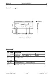
Transceiver module TRX433-10C2 / TRX868-10C2 (Vers. 1.0E) 5<br />
Dimensions<br />
0.5mm 24.5mm<br />
Pin description<br />
40.0mm<br />
TRX433-10<br />
TRX868-10<br />
front view<br />
14 13 12 11 10 9 8 7 6<br />
2 1<br />
2.54mm 10.16mm 2.54mm<br />
Lead frame: pins 0.5 x 0.2mm<br />
Pin Name I/O Description Level Condition<br />
4.5mm<br />
1 RF I/O RF- in/out for lambda / 4 antenna (~ 50 Ω) 0 V DC-path to GND<br />
2 GND RF Signal Ground<br />
6 V_P O Programming voltage (do not connect) VCC<br />
7 MCLR\ I Reset input, active low. 3 VCC Normal operation<br />
8 RSSI O Received Signal Strength Indicator (analog out) 0 V -128 dBm<br />
9 RTS O RTS handshake 0 V Ready to send<br />
10 TxD O UART transmit data (digital out) VCC Stop bit or no data<br />
11 RxD I UART receive data (digital in) VCC Stop bit or no data<br />
12<br />
CTS<br />
MODE<br />
WKUP<br />
I<br />
I<br />
I<br />
CTS handshake<br />
Interface mode (data or configuration)<br />
Sleep mode: Pin change terminates sleep<br />
13 V+ Positive supply voltage<br />
14 GND Ground<br />
0 V<br />
0 V<br />
Clear to send<br />
Data mode<br />
3.5 to 6VDC 4 or<br />
2.4 to 3.6VDC 5<br />
3<br />
connect an external reset controller, if supply voltage is not always within specified limits or if voltage<br />
ramp is slower than 50ms from 0V to 3.5V.<br />
4<br />
standard version with internal 3.3V supply voltage regulator (output logic high levels are limited to the<br />
internal 3.3V supply voltage)<br />
5<br />
version without internal voltage regulator (internal supply voltage = V+)
Transceiver module TRX433-10C2 / TRX868-10C2 (Vers. 1.0E) 6<br />
General information<br />
Serial Interface (RS232)<br />
There is a serial bidirectional full duplex interface available to communicate with the transceiver module. The<br />
data are transmitted and the transceiver module is configured over the same interface. You can choose<br />
between data mode and configuration mode with the MODE pin.<br />
Data mode (MODE Pin = Low)<br />
When the transceiver module receives data over the serial interface then those are automatically transmitted<br />
to all transceivers with the same configurations (frequency, RF data rate etc). Then those transceivers output<br />
them immediately over the serial interface after a few milliseconds. The baud rate for the RS232transmission<br />
can be set from 1.2kbaud to 115.2kbaud 6 .<br />
Configuration mode (MODE Pin = High)<br />
The transceiver module is configured over the serial interface. There is a comprehensive command set<br />
available. The last configuration will stay saved in the internal EEPROM if the accordant bit for saving in<br />
EEPROM is set. The configuration can occur in any baud rate from 1.2kbaud to 115.2kbaud 6 (the baud rate<br />
is detected automatically in the configuration mode).<br />
Radio transmission<br />
In the data mode, all the data which was received by the transceiver module over the serial interface are<br />
transmitted autonomous via radio. The transceiver module completely does the coding and decoding of the<br />
radio transmission. However, you can adjust the radio transmission to your own needs with help of a few<br />
simple commands. The following configurations can be done:<br />
Frequency selection<br />
There are 139 frequencies in 433MHz–band respectively 159 frequencies in 868MHz–band available, in<br />
each case in the 12.5 kHz–channel spacing. The frequency can be chosen irrespectively of the adjusted RF<br />
data rate. Make sure that on systems with several used frequencies, the frequency separation is at least the<br />
same as the occupied channels of the adjusted RF data rate (see table 1). This frequency separation has to<br />
be raised as high as possible for a better range.<br />
RF data rate<br />
The RF data rate can be chosen from 1.2kbits/s to 38.4kbits/s 7 according to requirements. The smaller the<br />
RF data rate is chosen, the higher is the radio range between the transceiver modules. RF data rates ><br />
19.2kbits/s are possible but they require an accordant dimensioned loop filter respectively a change in<br />
assembling. Through this change, the sensitivity of the receiver with low RF data rates is reduced. The basic<br />
model TRXnnn-10C2 is assembled with loop filters for max. 19.2kbits/s.<br />
Further radio transmission configurations to the chosen RF data rates are made automatically by the<br />
transceiver modules. These configurations for the different possible RF data rates can be found in table 1.<br />
RF data rates Coding Modulation FM-deviation IF-bandwidth Occupied<br />
channels<br />
1.2 kbit/s<br />
2.4 kbit/s<br />
4.8 kbit/s<br />
9.6 kbit/s<br />
19.2 kbit/s<br />
38.4 kbit/s 7<br />
Manchester GFSK<br />
Manchester GFSK<br />
NRZ GFSK<br />
NRZ GFSK<br />
NRZ GFSK<br />
NRZ GFSK<br />
NRZ GFSK<br />
NRZ GFSK<br />
+- 2.025 kHz<br />
+- 2.025 kHz<br />
+- 2.025 kHz<br />
+- 2.025 kHz<br />
+- 4.050 kHz<br />
+- 4.950 kHz<br />
+- 9.900 kHz<br />
+- 19.80 kHz<br />
9.6 kHz<br />
12.3 kHz<br />
9.6 kHz<br />
12.3 kHz<br />
19.2 kHz<br />
25.6 kHz<br />
51.2 kHz<br />
102.4 kHz<br />
1 x 12.5kHz<br />
1 x 12.5kHz<br />
1 x 12.5kHz<br />
1 x 12.5kHz<br />
2 x 12.5kHz<br />
4 x 12.5kHz<br />
8 x 12.5kHz<br />
12 x 12.5kHz<br />
Table 1 RF data rate with corresponding further configurations can be chosen.<br />
Comment<br />
433 MHz<br />
868 MHz<br />
433 MHz<br />
868 MHz<br />
6<br />
115.2kbaud requires a 16MHz µP clock frequency<br />
7<br />
RF data rate > 19.2kbits/s requires a modification of the loop filter, therefore a change in assembling and a<br />
16MHz µP clock frequency
Transceiver module TRX433-10C2 / TRX868-10C2 (Vers. 1.0E) 7<br />
Radio telegram structure<br />
For the radio transmission, the actual payloads are embedded in a radio telegram. The transceiver module<br />
builds the radio telegram and the associated coding and decoding and disburdens the user with that. A<br />
complete radio telegram is built according to figure 1.<br />
2ms Startup +<br />
Preamble<br />
Syncword<br />
2ms + 32 bits 24 bits 8 bits<br />
(opt.)<br />
Figure 1 structure of the radio telegram<br />
Functions of the individual blocks in the radio telegram<br />
LengthField<br />
DataField<br />
CRC16<br />
n x 8/9 bits (depends on fastsend-setting) 16 bits<br />
(opt.)<br />
2ms startup: settling time for the transmitter for the reduction of the transient emissions<br />
Preamble: allows the receiver to level out to the carrier signal of the transmitter<br />
Syncword: indiales start of the data transmission and conduces therefore to the receiver to synchronize<br />
LenthField: declares number of bytes payload in the DataField (optional)<br />
DataField: effective payload<br />
CDC16: checksum for payload in the data field (optional)<br />
Postamble: sends for the correct receiving of the last Data bits of the radio telegram<br />
Every radio telegram has to consist of 2ms Startup + Preamble, Syncword, DataField and Postamble. The<br />
blocks LengthField and CRC16 are, depending on the chosen configuration, added to the radio telegram as<br />
well. The duration of the individual blocks depends on the adjusted RF data rate and is calculated out of the<br />
number of bits multiplied by the bit duration of the adjusted RF data rate. Only the period of the 2ms Startup<br />
stays constantly 2ms with every RF data rate.<br />
Transmittion- and receiving buffer<br />
The transceiver module has a transmittion - and receiving buffer, 61 bytes each, for the serial interface.<br />
Transmittion buffer (TX-BUF)<br />
Over RS232 received data are buffered in the transmittion buffer. The space in the transmittion buffer frees<br />
byte-by-byte as soon as a byte is inserted into its place in the DataField of the radio telegramm.<br />
Receiving buffer (RX-BUF)<br />
In the receiving buffer, the over radio received data are buffered until their output over RS232. When the<br />
function “Output of the telegram-RSSI” respectively “Output of the no signal condition-RSSI” is enabled then<br />
these RSSI-values are buffered in the receiving buffer in addition to the payloads of the radio telegram.<br />
Depending on the configuration, there are maximum two additional bytes needed in the receiving buffer per<br />
radio telegram. The space in the receiving buffer for the receiving of the radio telegram has to be free by the<br />
time the radio telegram receives the actual payloads from the DataField. The space in the receiving buffer is<br />
freed byte-by-byte as soon as a byte is output over RS232.<br />
Postamble<br />
2 bits
Transceiver module TRX433-10C2 / TRX868-10C2 (Vers. 1.0E) 8<br />
Buffer overflow<br />
Be careful that the two buffers (transmittion- and receiving buffer) don’t overflow. That can be ensured by<br />
adhere the right timing or by using the handshake (see paragraph Example of data flow and Handshake with<br />
RTS/CTS).<br />
Overflow of the transmittion buffer<br />
The transmittion buffer has, additionally to its 61 bytes, a 2-byte overflow buffer. So when the transmittion<br />
buffer is full (61 bytes full) and further data are still transferred over RS232 then max. 2 bytes can be saved<br />
in the overflow buffer. Those will be transferred in the transmittion buffer as soon as there is space in there.<br />
When the overflow buffer is full as well then further over the RS232 received data will be rejected.<br />
Overflow of the receive buffer<br />
The receiving buffer has, additionally to its 61 bytes, a 2-byte overflow buffer. This buffer is only used for<br />
saving the RSSI-values in addition to the payload if the function “Output of the telegram-RSSI” respectively<br />
“output of the no signal condition-RSSI” is enabled and if the whole 61 bytes of the receiving buffer are full<br />
with the radio telegram.<br />
When data are received over radio even if the buffer is already full (61 bytes full), then the whole incoming<br />
radio telegram will be rejected if the CRC16 is on. If the CRC16 is off then the already received data will be<br />
saved and the rest of the incoming radio telegram will be rejected.<br />
Handshake with RTS/CTS<br />
The communication over the RS232-interface can be controlled with help of RTS/CTS to avoid overflowing of<br />
buffers. RTS and CTS are only used for the handshake when the handshake is activated. When the<br />
handshake is disabled then the RTS and CTS are ignored.<br />
Function RTS<br />
As soon as 61 bytes are saved in the transmittion buffer then the transceiver module stops the receiving of<br />
data over RS232 by setting the RTS-Pin on high. The user may not send further data over the RS232interface<br />
to the transceiver module until the RTS-pin changes to low again. The RS232-interface enables<br />
again (RTS-Pin reset to low) once ≤58 bytes are saved in the transmittion buffer.<br />
Function CTS<br />
With an activated handshake, the user can stop the output of data of the transceiver module by setting the<br />
CTS-Pin to high. The transceiver module doesn’t output any more data over the TxD-Pin until the CTS-Pin is<br />
set back to low by the user.<br />
Note<br />
If the CTS-Pin is used as handshake, don’t send any data to the transceiver module during the high-time of<br />
the CTS-Pin because these data would be interpreted as configuration data. The CTS-Pin has the double<br />
function handshake (CTS) and interface mode (MODE).<br />
Figure 2 shows the cycle of a data communication of 64 bytes with use of the handshake. There, module 1 is<br />
the transceiver and module 2 is the receiver. Additionally you can see how many bytes are saved in the<br />
transmittion buffer (TX-BUF) of the sending transceiver module and in the receiving buffer (RX-BUF) of the<br />
receiving transceiver module.<br />
module 1<br />
module 2<br />
bytes in TX-BUF ... 0........... 1........... ........60......... 61................................................................60.59.58.57.56. 56.55.55.54.53. 53.... ....3......................................................... 2...1...0..................................... ...............<br />
RS232, RTS-pin<br />
RS232, RxD-pin<br />
RF-transmission<br />
RS232, TxD-pin<br />
Byte 1<br />
Byte 2<br />
Byte 60<br />
Byte 61<br />
start RF-transmission<br />
after 2-3 bytes break<br />
32 Bit<br />
Preamble<br />
+2ms<br />
Startup<br />
24 Bit<br />
SYNC<br />
Byte 62<br />
Length<br />
Byte 1<br />
Byte 2<br />
Byte 3<br />
Byte 4<br />
Byte 5<br />
Byte 6<br />
Byte 7<br />
Byte 8<br />
Byte 9<br />
Byte 10<br />
Byte 11<br />
Byte 63<br />
Byte 64<br />
Byte 60<br />
Byte 61<br />
CRC16<br />
32 Bit<br />
Preamble<br />
+2ms<br />
Startup<br />
Byte 1<br />
Byte 2<br />
24 Bit<br />
SYNC<br />
Byte 3<br />
Length<br />
Byte 62<br />
Byte 63<br />
Byte 64<br />
bytes in RX-BUF ... 0......................... ........................................................................................................................................................... .................. 61.........60.........59.........58.........57.........56. 59... 58.......... .........0....<br />
Figure 2 data communication with handshake<br />
start RF-transmission<br />
after 2-3 bytes break<br />
Byte 4<br />
Byte 5<br />
CRC16<br />
Byte 6<br />
Byte 7<br />
Byte 64
Transceiver module TRX433-10C2 / TRX868-10C2 (Vers. 1.0E) 9<br />
CRC16<br />
The CRC16 is a 16-Bit check sum which checks the payloads in the DataField for correctnes. If the higher<br />
application doesn’t check the data then you should definitely use the CRC16.<br />
CRC16 off<br />
The radio data are not checked for correctness. The RS232 receives a data byte from the DataField of the<br />
radio telegram and outputs it immediately. The higher application has to deal with the checking of the data.<br />
CRC16 on<br />
The payloads in the DataField are CRC16-checksum-verified and the calculated checksum is included on<br />
the end of the radio telegram. That means that the data of the receiving transceiver module will only be<br />
output over RS232 when CRC16 corresponds. By wrong CRC16, the whole radio telegram will be rejected.<br />
Fast send<br />
The configuration Fast send decides when the radio transmission of the over the RS232 received payloads<br />
starts and in which way the radio telegram length is transmitted.<br />
Fast send off<br />
The data which were received in one piece over the RS232 are buffered in the transmittion buffer. As soon<br />
as no further data is received over the RS232 for the time of 2-3 RS232-bytes then the radio transmission<br />
starts and the current stored payloads in the transmittion buffer are transmitted. The length of the radio<br />
telegram is therefore defined at the beginning of the radio transmission (in the LengthField, the number of<br />
bytes of payloads are entered). When further data are received over RS232 during the radio transmission,<br />
they will be buffered in the transmittion buffer and they’ll build a new radio telegram as soon as the radio<br />
transmission of the current radio telegram is complete.<br />
Fast send on<br />
The radio transmission starts once the first byte is received over RS232 and will not stop until no byte is left<br />
in the transmittion buffer. Therefore the length of a radio telegram is not known in the beginning of the radio<br />
transmission. That’s why no LengthField is added to the radio telegram. To label the radio telegram length, a<br />
bit is added to every payload byte in the DataField which shows the end of the payloads.<br />
Note<br />
• Although the radio transmission starts earlier with Fast send than without, one bit is added to every<br />
payload byte in the DataField for the identification of the radio telegram length. Thereby, a radio telegram<br />
with fast send on and more than 8 bytes payload gets longer than one without fast send.<br />
• Due to the fact that Fast send means more computing effort, Fast send can only be used up to a RF data<br />
rate of 19.2kbits/s (respectively 9.6kbits/s by 8MHz µP clock frequency).<br />
• The radio telegram length is limited to 61 bytes with Fast send when CRC16 is enabled because the<br />
receiver has to buffer the whole radio telegram until CRC16 is checked. The user has to make sure that<br />
the length of the radio telegram is no more than 61 bytes payload.<br />
• With disabled CRC16 and Fast send on, a radio telegram length with over 61 bytes payload is possible.<br />
• The pause with the period of 2-3 RS232-bytes for the start of the radio transmission without Fast send<br />
varies depending on the adjusted configuration. To make sure that the radio transmission really will start<br />
you should keep a minimum pause of three RS232-bytes.
Transceiver module TRX433-10C2 / TRX868-10C2 (Vers. 1.0E) 10<br />
Examples of data flow<br />
Following, there are some examples by which you can see the data flow by different configuration of Fast<br />
send, CRC16, Handshake etc.<br />
Examples for different configuration of fast send and CRC16<br />
Refer to the figure for the data flow which depends on the configuration of Fast send and CRC16. Thereby,<br />
module 1 is used as transceiver and module 2 is used as receiver. Of course several modules with the same<br />
configuration as the transceiver can receive the data signal.<br />
module 1<br />
module 2<br />
RS232, RxD-pin<br />
RF-transmission<br />
RS232, TxD-pin<br />
Byte 1<br />
Byte 2<br />
Byte 3<br />
Byte 4<br />
start RF-transmission<br />
after 2-3 bytes break<br />
32 Bit<br />
Preamble<br />
+2ms<br />
Startup<br />
24 Bit<br />
SYNC<br />
Length<br />
Byte 1<br />
Byte 2<br />
Byte 3<br />
Byte 4<br />
CRC16<br />
Figure 3 Dataflow without Fast send with CRC16, RF data rate > RS232-baud rate<br />
module 1<br />
module 2<br />
RS232, RxD-pin<br />
RF-transmission<br />
RS232, TxD-pin<br />
Byte 1<br />
Byte 2<br />
Byte 3<br />
Byte 4<br />
start RF-transmission<br />
after 2-3 bytes break<br />
32 Bit<br />
Preamble<br />
+2ms<br />
Startup<br />
24 Bit<br />
SYNC<br />
Length<br />
Byte 1<br />
Byte 2<br />
Byte 3<br />
Byte 4<br />
Byte 1<br />
Byte 2<br />
Byte 1<br />
Byte 3<br />
output after first<br />
received databyte<br />
Figure 4 Dataflow without Fast send without CRC16, RF data rate > RS232-baud rate<br />
module 1<br />
module 2<br />
RS232, RxD-pin<br />
RF-transmission<br />
RS232, TxD-pin<br />
Byte 1<br />
Byte 2<br />
Byte 3<br />
Byte 4<br />
start RF-transmission<br />
after 2-3 bytes break<br />
2<br />
32 Bit<br />
Byte<br />
Preamble<br />
24 Bit<br />
+2ms Startup<br />
SYNC<br />
Figure 5 Dataflow without Fast send without CRC16, RF data rate < RS232-baud rate<br />
Length<br />
Byte 1<br />
Byte 1<br />
Byte 2<br />
Byte 3<br />
Byte 3<br />
Byte 4<br />
Byte 4<br />
output after first<br />
received databyte<br />
Byte 2<br />
Byte 3<br />
output after<br />
checked CRC16<br />
Byte 4<br />
Byte 4
Transceiver module TRX433-10C2 / TRX868-10C2 (Vers. 1.0E) 11<br />
module 1<br />
module 2<br />
RS232, RxD-pin<br />
RF-transmission<br />
RS232, TxD-pin<br />
Byte 1<br />
Byte 2<br />
32 Bit<br />
Preamble<br />
+2ms<br />
Startup<br />
Byte 3<br />
24 Bit<br />
SYNC<br />
Byte 4<br />
Byte 1<br />
Byte 2<br />
Byte 3<br />
Byte 4<br />
start RF-transmission after<br />
first received RS232-byte<br />
CRC16<br />
Byte 1<br />
Byte 2<br />
Byte 3<br />
output after<br />
checked CRC16<br />
Figure 6 Dataflow with Fast send with CRC16, RF data rate > RS232-baud rate<br />
module 1<br />
module 2<br />
RS232, RxD-pin<br />
RF-transmission<br />
RS232, TxD-pin<br />
Byte 1<br />
Byte 2<br />
32 Bit<br />
Preamble<br />
+2ms<br />
Startup<br />
Byte 3<br />
24 Bit<br />
SYNC<br />
Byte 4<br />
Byte 1<br />
Byte 2<br />
Byte 3<br />
Byte 4<br />
start RF-transmission<br />
after first received RS232-byte<br />
Byte 1<br />
Byte 2<br />
Byte 3<br />
output after first<br />
received databyte<br />
Figure 7 Dataflow with Fast send without CRC16, RF data rate > RS232-baud rate<br />
module 1<br />
module 2<br />
RS232, RxD-pin<br />
RF-transmission<br />
RS232, TxD-pin<br />
Byte 1<br />
Byte 2<br />
Byte 3<br />
Byte 4<br />
2<br />
32 Bit<br />
Byte<br />
Preamble<br />
24 Bit<br />
+2ms Startup<br />
SYNC<br />
start RF-transmission after<br />
first received RS232-byte<br />
Byte 1<br />
Byte 1<br />
Byte 4<br />
Byte 2<br />
Byte 3<br />
Byte 3<br />
Byte 4<br />
output after first<br />
received databyte<br />
Figure 8 Dataflow with Fast send without CRC16, RF data rate < RS232-baud rate<br />
Byte 4<br />
Byte 4
Transceiver module TRX433-10C2 / TRX868-10C2 (Vers. 1.0E) 12<br />
Example for a continued radio data stream (radio telegram with more than 61 bytes payload)<br />
A continued radio data stream (thus a telegram which isn’t limited to 61 bytes payload) can only be realized<br />
with Fast send and without CRC16. Also, the RS232-baud rate has to be chosen at least as fast as the RF<br />
data rate. With these configurations, a continued radio data stream like in figure 9 can be realized. It is also<br />
apparent in Figure 9 how the CTS pin may prevent the transceiver module from outputting the data via<br />
RS232 that it received via radio. Also you can see the number of bytes in the transmittion buffer (TX-BUF) of<br />
the sending transceiver module and the numbers of bytes in the receiving buffer (RX-BUR) of the receiving<br />
transceiver module.<br />
module 1<br />
module 2<br />
bytes in TX-BUF<br />
RS232, RTS-pin<br />
RS232, RxD-pin<br />
RF-transmission<br />
RS232, TxD-pin<br />
RS232, CTS-pin<br />
bytes in RX-BUF<br />
0.... 1.... 2.... 3.... 4.... 5.... 6.... 7.... 8.... 9....10...11...12...12...12...13...13...14...14...15...15...<br />
Byte 1<br />
Byte 2<br />
Byte 3<br />
Byte 4<br />
32 Bit<br />
Preamble<br />
+2ms Startup<br />
Byte 5<br />
Byte 6<br />
Byte 7<br />
Byte 8<br />
Byte 9<br />
Byte 10<br />
24 Bit<br />
SYNC<br />
Byte 11<br />
Byte 12<br />
Byte 13<br />
Byte 1<br />
Byte 14<br />
Byte 15<br />
Byte 2<br />
Byte 16<br />
Byte 17<br />
Byte 3<br />
Byte 18<br />
Byte 19<br />
Byte 4<br />
Byte 20<br />
... 0........................................................................................ 1....0....1....0.... 1....0....1....0... ....0....1....0....1....0....1..........2..........3...2.....2....1...2.1...0..1....0....1....0....1....0..<br />
Figure 9 Dataflow with Fast send without CRC16, RS232-baud rate = 2x RF data rate<br />
Byte 5<br />
Byte 21<br />
Byte 121<br />
60...60...61. 60........59........ 58...59...59...60...60...61.60.... 59........58... 59...59...<br />
Example for continued data stream over RS232<br />
With Fast send enabled and CRC16 disabled, a continued data stream can be realized over the RS232interface.<br />
For that, the RF data rate has to be chosen higher than the RS232-baud rate. In figure 10, a<br />
continued data stream over RS232 is shown by which the RF data rate is adjusted twice as fast as the<br />
RS232-baud rate. Further you can see how many bytes are stored in the transmittion buffer (TX-BUF) of the<br />
sending transceiver module and in the receiving buffer (RX-BUF) of the receiving transceiver module.<br />
module 1<br />
module 2<br />
bytes in TX-BUF<br />
RS232, RTS-pin<br />
RS232, RxD-pin<br />
RF-transmission<br />
RS232, TxD-pin<br />
RS232, CTS-pin<br />
bytes in RX-BUF<br />
Byte 1<br />
Byte 2<br />
Byte 3<br />
Byte 4<br />
...0........... 1...........2...........3........ 2. . 3. 2...1..2.1...0....1...........2...........3......... 2.3..2....1.2...1...0..1...........2...........3..........4.3...2.... 2...1...0.1...........2...........3...........4..3...2..3. 2...<br />
Byte 1<br />
Byte 2<br />
32 Bit<br />
Preamble<br />
+2ms<br />
Startup<br />
Byte 3<br />
24 Bit<br />
SYNC<br />
Byte 4<br />
Byte 1<br />
Byte 5<br />
Byte 2<br />
Byte 3<br />
Byte 4<br />
Byte 5<br />
Byte 1<br />
Byte 6<br />
Byte 7<br />
Byte Byte 1 8<br />
32 Bit<br />
Preamble<br />
+2ms<br />
Startup<br />
Byte Byte 1 9<br />
24 Bit<br />
SYNC<br />
Byte Byte 1 10<br />
...0....................................................... 1... 2...3.2..3...4..3.......... 2...........1.......... 0.1...2...3.2..3...4..3.......... 2...........1..........0.1...2...3.2..3...4..3.......... 2...........1...........0.1.... 2...<br />
Byte 60<br />
Byte Byte 1 11<br />
Byte 6<br />
Byte 7<br />
Byte 8<br />
Byte 9<br />
Byte 10<br />
Byte 61<br />
Byte 122<br />
Byte 123<br />
Byte 61<br />
Byte Byte 1 12<br />
Byte 62<br />
Byte 62<br />
Byte 63<br />
Byte Byte 1 13<br />
32 Bit<br />
Preamble<br />
+2ms<br />
Startup<br />
Byte 64<br />
Byte Byte 1 14<br />
24 Bit<br />
SYNC<br />
Byte 124<br />
Byte 65<br />
Byte Byte 1 15<br />
Byte 125<br />
Byte 63<br />
Byte 126<br />
Byte 66<br />
Byte 64<br />
Byte 127<br />
Byte Byte 1 16<br />
Byte 11<br />
Byte 12<br />
Byte 13<br />
Byte 14<br />
Byte 15<br />
Figure 10 Data stream with Fast send without CRC16, RF data rate = 2x RS232-baud rate<br />
Byte 2<br />
Byte 3<br />
Byte 4<br />
Byte 5<br />
Byte 6<br />
Byte 7<br />
Byte Byte 1 8<br />
Byte Byte 1 9<br />
Byte Byte 1 10<br />
Byte Byte 1 11<br />
Byte 65<br />
Byte 128<br />
Byte 67<br />
Byte Byte 1 12<br />
Byte 66<br />
Byte Byte 1 17<br />
Byte 67<br />
Byte 68<br />
Byte Byte 1 18<br />
32 Bit<br />
Preamble<br />
+2ms<br />
Startup<br />
Byte Byte 1 13<br />
Byte 68<br />
Byte 69<br />
Byte Byte 1 14<br />
Byte 129<br />
Byte 69<br />
Byte Byte 1 19<br />
Byte 70<br />
24 Bit<br />
SYNC<br />
Byte 130<br />
Byte Byte 1 15<br />
Byte 70<br />
Byte Byte 1 20<br />
Byte 16<br />
Byte 71<br />
Byte 17<br />
Byte 131 60<br />
Byte 16<br />
Byte 21<br />
Byte 18
Transceiver module TRX433-10C2 / TRX868-10C2 (Vers. 1.0E) 13<br />
RSSI of the telegram and no signal condition-RSSI<br />
To define the quality of a radio connection, the received sighnal strength indicator (RSSI) of the just received<br />
radio telegram can be output over RS232 after every received radio telegram. The signal strength will be<br />
output in dBm in addition to the payloads of the radio telegram in a twos complement.<br />
The no signal condition - RSSI can be output optionally in addition to the RSSI of the telegram. The RSSIvalue<br />
which was measured immediately after the radio telegram will be output as a no signal condition -<br />
RSSI. Out of those two RSSI-values, the signal-noise ratio can be calculated. Of course, the no signal<br />
condition-RSSI can be read out with the command “READ RSSI current” as well. You can see the output of<br />
the telegram-RSSI (RSSI TLG) and of the no signal condition-RSSI (RSSI at no signal condition) added to<br />
the payload in figure 11.<br />
Note<br />
When the function “Output of the telegram-RSSI” respectively “Output of the no signal condition - RSSI” is<br />
enabled, then those RSSI-values are buffered in the receive buffer of the transceiver following the payload<br />
until they are output over RS232. Depending on the configuration, maximum 2 additional bytes are needed in<br />
the receive buffer per radio telegram.<br />
module 1<br />
module 2<br />
RS232, RxD-pin<br />
RF-transmission<br />
RS232, TxD-pin<br />
Byte 1<br />
Byte 2<br />
Byte 3<br />
Byte 4<br />
start RF-transmission<br />
after 2-3 bytes break<br />
32 Bit<br />
Preamble<br />
+2ms<br />
Startup<br />
24 Bit<br />
SYNC<br />
Length<br />
Byte 1<br />
Byte 2<br />
Byte 3<br />
Byte 4<br />
Figure 11 Output of the telegram-RSSI and the no signal condition-RSSI<br />
CRC16<br />
Byte 1<br />
Byte 2<br />
Byte 3<br />
output after<br />
checked CRC16<br />
Byte 4<br />
RSSI TLG<br />
RSSI Ruhe
Transceiver module TRX433-10C2 / TRX868-10C2 (Vers. 1.0E) 14<br />
Recalibration<br />
The VCO has to be recalibrated by a temperature variation of >40°C or by a variation of the supply voltage of<br />
> 0.25 volt (for version without voltage regulator). It can be calibrated automatically in defined intervals from<br />
5 to 150min, by temperature differences of more than 20°C or just once manual during the calibration<br />
command. During the calibration, which normally takes 50ms, no radio communicationl is possible.<br />
Beginning, end and result will be reported if the module is in the configuration mode.<br />
There occurs an automatic calibration with every power up. The last calibration stays stored in the RAM<br />
during the sleep. Therefore the transceiver is ready again pretty fast after the wakeup (by 19.2kbits/s RF<br />
data rate after 3ms, by 2.4kbits/s RF data rate after 5ms). When the temperatures or the supply voltage can<br />
change significantly during the sleep then you first have to recalibrate after the wake up.<br />
Energy-saving mode and characteristics by reset, power up, wake up und sleep<br />
The RF-part of the transceiver can be enabled and disabled with the command Power-control, as well as<br />
the LED. Disabled, the current consumption is highly reduced but the processor still stays active and uses<br />
electricity.<br />
The sleep command is for battery operated units which are mostly inactive and which may just use electricity<br />
during the radio communication. Thereby the current consumption can be reduced down to 3µA (version<br />
without intern voltage regulator) during the sleep. The version with voltage regulator uses ca. 100µA while<br />
sleeping. During the sleep, the transceiver is inactive but all the configurations and the last calibration remain<br />
in the RAM.<br />
High reserve energy is achievable due to the low current consumption during the sleep and the short setuptime<br />
after a wakeup of 3ms by 19.2kbits/s RF data rate respectively 5ms by 2.4kbits/s RF data rate because<br />
the average of the current consumption depends almost only on the proportion transmitting time/transmitting<br />
interval.<br />
The sleep command disables the RF-part and the LED and stops afterwards the clock of the micro controller.<br />
The behavior during the sleep as well as the behavior after a wakeup can be defined with the command<br />
parameter WKUP_mode of the sleep command. The timer for automatic recalibration is paused during the<br />
sleep.<br />
The WKUP-Pin has to be on its sleep-level (high or low) before the sleep but at the latest 50µs after the<br />
answer to the sleep command. Afterwards, the change in level automatically activates an immediate<br />
wakeup.<br />
The command power up mode is similar to the sleep command. The sleep command is performed<br />
immediately, the command power up mode doesn’t affects until the next power up. The transceiver can be<br />
configured with PWUP_mode so that it automatically changes to the sleep mode after the power up until it’s<br />
awoken and reconfigured from outside. This is important in battery operations so that the radio module<br />
doesn’t get active autonomously after a battery change and discharges the battery unnoticed.<br />
The sleep mode finishes through a pinchange on the WKUP-Pin. Thereby, the program either continues<br />
where it was interrupted by the sleep-command or there is an internal reset whereat a complete re-start<br />
occurs. When the transceiver is in the configuration mode (MODE-Pin = High) then it shows by “REPORT<br />
READY” on the RS232 that the microcontroller on the transceiver is ready. Alternatively, the RTS-Pin can be<br />
supervised. The RTS-Pin goes back to high after the sleep-command. The RTS-Pin is set back to low as<br />
soon as the transceiver is ready again after a wakeup (see figure 12 and 13).
Transceiver module TRX433-10C2 / TRX868-10C2 (Vers. 1.0E) 15<br />
RTS-pin<br />
MODE-pin and<br />
WKUP-pin resp.<br />
RS232, RxD-pin<br />
RS232, TxD-pin<br />
0B0H<br />
020H<br />
sleepcommand<br />
change to<br />
config-mode<br />
021H<br />
answer<br />
(only sent if still<br />
in config-mode)<br />
020H<br />
021H<br />
enter sleep<br />
030H<br />
wakeup (pinchange<br />
on WKUP-pin)<br />
max. 50us for pinchange, otherwise interpreted as wakeup<br />
001H<br />
ready after wakeup<br />
(only sent in config-mode)<br />
ready after wakeup<br />
Figure 12 Sleep and wake up with configuration mode after wake up<br />
RTS-pin<br />
MODE-pin and<br />
WKUP-pin resp.<br />
RS232, RxD-pin<br />
RS232, TxD-pin<br />
0B0H<br />
020H<br />
sleepcommand<br />
change to<br />
config-mode<br />
021H<br />
answer<br />
(only sent if still<br />
in config-mode)<br />
020H<br />
021H<br />
enter sleep<br />
030H<br />
wakeup (pinchange<br />
on WKUP-pin)<br />
Figure 13 Sleep and wakeup with data mode after wake up<br />
001H<br />
ready after wakeup<br />
ready after wakeup<br />
(suppressed because in data-mode)<br />
The transceiver module will report after ca. 175ms with a ready signal over RS232 after a power up if the<br />
transceiver module is in the configuration mode. A negative edge on the RTS-Pin can be used alternatively<br />
to it as a ready signal (see figure 14 respectively figure 15).<br />
VCC<br />
RTS-pin<br />
MODE-pin<br />
RS232, TxD-pin<br />
VCC on<br />
change to config-mode<br />
030H<br />
000H<br />
ready ca. 175ms<br />
after powerup<br />
ready ca. 175ms after powerup<br />
(only sent in config-mode)<br />
Figure 14 Powerup with transceiver module in configuration mode
Transceiver module TRX433-10C2 / TRX868-10C2 (Vers. 1.0E) 16<br />
VCC<br />
RTS-pin<br />
MODE-pin<br />
RS232, TxD-pin<br />
VCC on<br />
stay in data-mode<br />
Figure 15 Powerup with transceivermodul in data mode<br />
030H<br />
000H<br />
ready ca. 175ms<br />
after powerup<br />
ready ca. 175ms after powerup<br />
(suppressed because in data-mode)<br />
Note<br />
• Pay attention to the paragraph supply voltage and MCLR/Reset whenever the supply switches!<br />
• The most capacity of battery can generally be saved with the sleep-function. We recommend using the<br />
sleep-function instead of switching the supply.
Transceiver module TRX433-10C2 / TRX868-10C2 (Vers. 1.0E) 17<br />
RSSI (Received Signal Strength Indicator)<br />
There is a voltage on pin 8 (RSSI) which is directly proportional to the RF - field strength. The transceiver<br />
scans the field strength every 3ms and outputs the RSSI-value as analogue voltage to pin 8.<br />
The voltage on the RSSI-pin follows this equation:<br />
Urssi<br />
1.5 * 3.3V<br />
PRF [dBm] = − 128 + * 127<br />
Zero-point by -128 dBm, Slope: 25.7dB/V, Measurement range -120…-60 dBm<br />
The RSSI-pin shows an internal resistance of ca. 10kΩ<br />
RSSI characteristic<br />
-140 -130 -120 -110 -100 -90 -80 -70 -60 -50 -40 -30 -20 -10 0<br />
Phf [dBm]<br />
Figure 16 Tension on RSSI-pin<br />
PRF can be read out digitally as a RSSI value with the command “READ RSSI current”, whereat the value is<br />
output directly in the twos complement in the unit dBm<br />
Examples: PRF = -128 dBm makes a RSSI of 128dec respectively 080H (under the noise floor)<br />
PRF = -120 dBm makes a RSSI of 136dec respectively 088H<br />
PRF = -110 dBm makes a RSSI of 146dec respectively 092H<br />
PRF = -100 dBm makes a RSSI of 156dec respectively 09CH<br />
PRF = -60 dBm makes a RSSI of 196dec respectively 0C4H (saturation limit)<br />
The maximal value of the RSSI will be saved by the transceiver (peak hold) and can be read out as well with<br />
the command “READ RSSI peak” as well. Every read operation of the RSSI peak initializes thereby the<br />
maximal value so that the maximal value represents the period between two read operations. The RSSI<br />
peak is initialized right after a sleep as well.<br />
The RSSI current and the RSSI peak go back to -128dBm during transmission<br />
3.50<br />
3.00<br />
2.50<br />
2.00<br />
1.50<br />
1.00<br />
0.50<br />
0.00
Transceiver module TRX433-10C2 / TRX868-10C2 (Vers. 1.0E) 18<br />
Power supply<br />
The radio transceiver with the voltage regulator needs a good supply voltage with minimum 3.5V and a ripple<br />
of < 10mVpp. The power amplifier is directly located on the input side of the supply voltage. The<br />
transmission power is therefore to a minor degree dependant on supply voltage. When the supply is<br />
switched then the voltage has to fall back to 0V after disabling it before you can enable it again. The supply<br />
voltage has to rise from 0V to 3.5V during max 50ms so that the integrated microcontroller starts correctly.<br />
The voltage can never fall under 3.3 Volt, not even momentary. If this can’t be guaranteed then the supply<br />
has to be supervised with a voltage detector. As soon as it falls under ca. 3.3V, the input MCLR\ has to be<br />
pulled down. See application example with Demokit3.<br />
The radio transceiver without voltage regulator can operate from 2.4V to 3.6V. Keep a ripple of 3.3Volt (for standard TRX with 3.3V<br />
internal voltage regulator). The trip voltage can be reduced down to 2.3V by versions without a voltage<br />
regulator and a reduced µP clock frequency.<br />
When you follow the under the paragraph Power supply listed points then there is no external voltage<br />
detector necessary.<br />
After a reset on MCLR\Reset input, the transceiver normally needs 75ms to the output of the ready signal<br />
because the transceiver is calibrated and configured automatically after a reset. The ready signal will only be<br />
output if the module is in the configuration mode.<br />
Status LED<br />
The status of the transceiver-LED is defined by the command power-control. When that command<br />
accomplished with a set Bit7 then the LED will enable or disable by a powerup accordingly.<br />
After a sleep-command the LED is always turned off and after the wakeup the LED is always set back to the<br />
status it had before the sleep.
Transceiver module TRX433-10C2 / TRX868-10C2 (Vers. 1.0E) 19<br />
Temperature sensor<br />
The transceiver module has an internal temperature sensor. The current temperature can be read by the<br />
command “READ temperature”. The value range is in between -40°C to +115°C. The temperature is<br />
actualized every 5s, no matter how often it is read.<br />
Note<br />
The 5s-timer for the actualization of the temperature is stopped during the sleep. After the sleep, the<br />
temperature which was read before the sleep can therefore be displayed for 5s. This temperature can differ<br />
from the current temperature by a long sleep-time.
Transceiver module TRX433-10C2 / TRX868-10C2 (Vers. 1.0E) 20<br />
Technical data TRX433-10C<br />
Frequency range 433.0625.... 434.7875 MHz (12.5 kHz channel spacing)<br />
RF data rate<br />
Possible parameterization<br />
of the RF data rate with the<br />
corresponding fixed<br />
configuration.<br />
Coding Occupied<br />
channel<br />
IF-bandwidth FM-Deviation<br />
(Standard version up to<br />
19.2kbits/s 8 1.2 kbit/s<br />
2.4 kbit/s<br />
4.8 kbit/s<br />
)<br />
9.6 kbit/s<br />
19.2 kbit/s<br />
38.4 kbit/s 8<br />
Manchester 1 x 12.5 kHz<br />
NRZ 1 x 12.5 kHz<br />
NRZ 2 x 12.5 kHz<br />
9.6 kHz<br />
9.6 kHz<br />
19.2 kHz<br />
+- 2.025 kHz<br />
+- 2.025 kHz<br />
+- 4.050 kHz<br />
NRZ<br />
NRZ<br />
NRZ<br />
4 x 12.5 kHz<br />
8 x 12.5 kHz<br />
12 x 12.5 kHz<br />
25.6 kHz<br />
51.2 kHz<br />
102.4 kHz<br />
+- 4.950 kHz<br />
+- 9.900 kHz<br />
+- 19.80 kHz<br />
-120 dBm with RF data rate = 1.2kbit/s<br />
Receiver sensitivity by<br />
different parameterization<br />
(50 Ohm / BER = 1E-3)<br />
-118 dBm<br />
-115 dBm<br />
-113 dBm<br />
-110 dBm<br />
-106 dBm<br />
with RF data rate = 2.4kbit/s<br />
with RF data rate = 4.8kbit/s<br />
with RF data rate = 9.6kbit/s<br />
with RF data rate = 19.2kbit/s<br />
with RF data rate = 38.4kbit/s 8<br />
Frequency tolerance<br />
± 5ppm standard (Temp. -10°C ... +60°C)<br />
± 2ppm optional (Temp. -10°C ... +60°C)<br />
Transmission power<br />
+12 dBm, supply 5.0 V<br />
+10 dBm, supply 3.5 V<br />
Modulation GFSK<br />
Radio range by<br />
free sight 9<br />
2000m with RF data rate = 1.2kbit/s<br />
efficient instruction set<br />
supports functions like:<br />
Power-control, defines behavior by Power up, sleep, standby<br />
calibration, RSSI-output, read module temperature, read and write register,<br />
direct EEPROM-access (read, write),<br />
Serial number, Hardware, Software version etc.<br />
serial over RS232 with TTL level, 8 Data bits, 1 Stop bit, no parity<br />
baud rates: 1.2 / 2.4 / 4.8 / 9.6 / 19.2 / 38.4 / 57.6 / 115.2<br />
Data interface<br />
10 kbaud<br />
automatic baud rate detection on configuration<br />
Handshake with RTS/CTS<br />
61 bytes transmittion buffer and receive buffer<br />
supply<br />
3.5 to 6 V DC not stabilized, Ripple
Transceiver module TRX433-10C2 / TRX868-10C2 (Vers. 1.0E) 21<br />
Technical data TRX868-10C<br />
Frequency range 868.0125.... 869.9875 MHz (12.5 kHz channel spacing)<br />
RF data rate<br />
Possible parameterization<br />
of the RF data rate with the<br />
corresponding fixed<br />
configuration<br />
coding Occupied<br />
channels<br />
IF-bandwidth FM-Deviation<br />
(Standard version up to<br />
19.2kbits/s 11 1.2 kbit/s<br />
2.4 kbit/s<br />
4.8 kbit/s<br />
)<br />
9.6 kbit/s<br />
19.2 kbit/s<br />
38.4 kbit/s 11<br />
Manchester 1 x 12.5 kHz<br />
NRZ 1 x 12.5 kHz<br />
NRZ 2 x 12.5 kHz<br />
9.6 kHz<br />
9.6 kHz<br />
19.2 kHz<br />
+- 2.025 kHz<br />
+- 2.025 kHz<br />
+- 4.050 kHz<br />
NRZ<br />
NRZ<br />
NRZ<br />
4 x 12.5 kHz<br />
8 x 12.5 kHz<br />
12 x 12.5 kHz<br />
25.6 kHz<br />
51.2 kHz<br />
102.4 kHz<br />
+- 4.950 kHz<br />
+- 9.900 kHz<br />
+- 19.80 kHz<br />
Receiver sensitivity(50 Ohm -115 dBm<br />
/ BER = 1E-3)<br />
With RF data rate= 1.2kbit/s<br />
Frequency tolerancee<br />
± 5ppm standard (Temp. -10°C ... +60°C)<br />
± 2ppm optional (Temp. -10°C ... +60°C)<br />
Transmission power<br />
+10 dBm, supply 5.0 V<br />
+ 8 dBm, supply 3.5 V<br />
Modulation GFSK<br />
Radio range<br />
by free sight 12<br />
1200m with RF data rate = 1.2kbit/s<br />
efficient instruction set<br />
supports functions like:<br />
Power-control, defines behavior by Power up, sleep, standby<br />
calibration, RSSI-output, read module temperature, read and write register,<br />
direct EEPROM-access (read, write),<br />
Serial number, Hardware, Software version etc.<br />
serial over RS232 wit TTL level, 8 Data bits, 1 Stop bit, no parity<br />
baud rates: 1.2 / 2.4 / 4.8 / 9.6 / 19.2 / 38.4 / 57.6 / 115.2<br />
Data interface<br />
13 kbaud<br />
automatic baud rate detection on configuration<br />
Handshake with RTS/CTS<br />
61 bytes transmittion buffer and receive buffer<br />
supply<br />
3.5 to 6 V DC not stabilized, Ripple
Transceiver module TRX433-10C2 / TRX868-10C2 (Vers. 1.0E) 22<br />
Radio range<br />
The radio range depends on several conditions, which depend on the actual location.<br />
Most important factors are: The height of the antenna above ground, electromagnetically noise near the<br />
receiver (from PC’s, monitors etc.), other radio transmittions, type of ground, transmittions within the same<br />
frequency band on adjacent channels.<br />
Under normal conditions, with a Demokit3 by 433MHz and the lowest RF data rate, an operating distance of<br />
over 4km was measured in hilly area. Therefore the stated values are rather conservative.<br />
When the maximal ranges in the open country are important then we recommand the 433MHz frequency<br />
band. When there is already a system with 433MHz used on the actual location then you might have higher<br />
ranges with the 868MHz than with the 433MHz.<br />
The in the technical data indicated range is conservative and measured with the Demokit3 in a hilly area.
Transceiver module TRX433-10C2 / TRX868-10C2 (Vers. 1.0E) 23<br />
simplified schematic TRXnnn-10<br />
VCC_IN<br />
CTS<br />
RxD<br />
TxD<br />
RTS<br />
R4<br />
7 8<br />
5<br />
6<br />
3<br />
4<br />
1<br />
2<br />
F1<br />
1<br />
7<br />
8<br />
9<br />
3<br />
4<br />
5<br />
6 10<br />
VCC<br />
330R<br />
47R / 100p<br />
C35<br />
RSSI<br />
R1<br />
100n<br />
VCC<br />
10k<br />
C38<br />
100n<br />
GND<br />
TP14<br />
V+<br />
TP13<br />
CTS<br />
TP12<br />
RxD<br />
TP11<br />
TxD<br />
TP10<br />
RTS<br />
TP9<br />
R2<br />
RSSI<br />
TP8<br />
TP7<br />
100R<br />
MCLR<br />
V_P<br />
TP6<br />
VCC<br />
2<br />
RF-part with CC1020<br />
16<br />
15<br />
6<br />
5<br />
VSS<br />
VSS<br />
R11<br />
10k<br />
VDD<br />
VDD<br />
CTS<br />
RTS<br />
PCLK<br />
PSEL<br />
14<br />
13<br />
12<br />
11<br />
RB7/T1OSI<br />
RB6/T1OSO/T1CKI<br />
RB5<br />
RB4/PGM<br />
RA5/MCLR/THV<br />
4<br />
MCLR<br />
R12<br />
C34<br />
10n<br />
100R<br />
PCLK<br />
PSEL<br />
10<br />
9<br />
8<br />
7<br />
RA4/T0CKI/CMP2<br />
3<br />
RSSI<br />
TxD<br />
RxD<br />
DCLK<br />
LOCK<br />
DCLK<br />
RB3/CCP1<br />
RB2/TX/CK<br />
RB1/RX/DT<br />
INT/RB0<br />
TP2<br />
GND<br />
DIO<br />
PDIO<br />
LED<br />
SDA<br />
2<br />
1<br />
20<br />
19<br />
TP1<br />
DIO<br />
PDIO<br />
RA3/AN3/CMP1<br />
RA2/AN2/VR<br />
RA1/AN1<br />
RA0/AN0<br />
ANT<br />
RF<br />
RA6/OSC2/CLKOUT<br />
17<br />
Y2<br />
RA7/OSC1/CLKIN<br />
18<br />
JMP1<br />
n.f.(4k7)<br />
Vers. TRXxxx-10-xx : 16MHz<br />
Vers. TRXxxx-11-xx : 8MHz<br />
U3<br />
PIC16LF648A-I/SS<br />
R13<br />
330R<br />
V_PA VCC<br />
R15<br />
47k<br />
LED1<br />
KM-27SRD-09<br />
R16<br />
Standard: U5 fitted, R16 not fitted<br />
Optional: U5 not fitted, R16 fitted<br />
n.f. (0R)<br />
U5<br />
LP2980IM5-3.3<br />
L9<br />
5<br />
Vout<br />
Vin<br />
1<br />
VCC_IN<br />
On/Off<br />
3<br />
C36<br />
10u/10V<br />
N/C<br />
GND<br />
C37<br />
100n<br />
TRX433-xx-xx / TRX868-xx-xx<br />
4<br />
2<br />
Title:<br />
Processor-part with PIC16LF648A<br />
File: TRX-Simplified 1.5.SchDoc<br />
Date: 26.02.2009 REV 1.5 Sheet 1 of 1
Transceiver module TRX433-10C2 / TRX868-10C2 (Vers. 1.0E) 24<br />
Example of use for TRXnnn-10C<br />
VCC<br />
C1<br />
Levelshift necessary, if levels are not 100% compatible<br />
100n<br />
MOD1<br />
VDD<br />
3.3V logic levels 5V logic levels<br />
on Transceiver side on controller side<br />
VSS<br />
C2<br />
10u/10V<br />
VCC<br />
14<br />
GND<br />
13<br />
V+<br />
WAKEUP / MODE / CTS<br />
12<br />
Y1<br />
5V logic output<br />
R1 1k<br />
WKUP / MODE / CTS<br />
OSC1<br />
5V logic output<br />
TxD<br />
R2 1k<br />
11<br />
RxD<br />
OSC2<br />
3.3V-logic compatible input<br />
RxD<br />
10<br />
TxD<br />
8MHz<br />
3.3V-logic compatible input<br />
RTS<br />
9<br />
RTS<br />
analog input<br />
RSSI<br />
8<br />
RSSI<br />
RESET<br />
7<br />
MCLR<br />
6<br />
V_P<br />
Microcontroller<br />
U1<br />
R4<br />
2<br />
1<br />
VCC VDD RES<br />
VCC<br />
3<br />
C3 10k<br />
VSS<br />
10n<br />
S-80833CNMC<br />
reset level 3.3V<br />
2<br />
GND<br />
1<br />
RF<br />
J1 MCX/BNC<br />
TRX433/868-10C<br />
VCC<br />
U2 LM7805<br />
VI VO<br />
+Supply<br />
C6<br />
10u/10V<br />
C5<br />
100n<br />
GND<br />
C4<br />
330n<br />
TRX433/868-10C<br />
Title:<br />
Application example<br />
File: Application 10C_V1.SCHDOC<br />
Date: 16.02.2009 REV 1.0 Sheet 1 of 1
Transceiver module TRX433-10C2 / TRX868-10C2 (Vers. 1.0E) 25<br />
Frequency table TRX433-10C<br />
1 433.0625 MHz 36 433.5000 MHz 71 433.9375 MHz 106 434.3750 MHz<br />
2 433.0750 MHz 37 433.5125 MHz 72 433.9500 MHz 107 434.3875 MHz<br />
3 433.0875 MHz 38 433.5250 MHz 73 433.9625 MHz 108 434.4000 MHz<br />
4 433.1000 MHz 39 433.5375 MHz 74 433.9750 MHz 109 434.4125 MHz<br />
5 433.1125 MHz 40 433.5500 MHz 75 433.9875 MHz 110 434.4250 MHz<br />
6 433.1250 MHz 41 433.5625 MHz 76 434.0000 MHz 111 434.4375 MHz<br />
7 433.1375 MHz 42 433.5750 MHz 77 434.0125 MHz 112 434.4500 MHz<br />
8 433.1500 MHz 43 433.5875 MHz 78 434.0250 MHz 113 434.4625 MHz<br />
9 433.1625 MHz 44 433.6000 MHz 79 434.0375 MHz 114 434.4750 MHz<br />
10 433.1750 MHz 45 433.6125 MHz 80 434.0500 MHz 115 434.4875 MHz<br />
11 433.1875 MHz 46 433.6250 MHz 81 434.0625 MHz 116 434.5000 MHz<br />
12 433.2000 MHz 47 433.6375 MHz 82 434.0750 MHz 117 434.5125 MHz<br />
13 433.2125 MHz 48 433.6500 MHz 83 434.0875 MHz 118 434.5250 MHz<br />
14 433.2250 MHz 49 433.6625 MHz 84 434.1000 MHz 119 434.5375 MHz<br />
15 433.2375 MHz 50 433.6750 MHz 85 434.1125 MHz 120 434.5500 MHz<br />
16 433.2500 MHz 51 433.6875 MHz 86 434.1250 MHz 121 434.5625 MHz<br />
17 433.2625 MHz 52 433.7000 MHz 87 434.1375 MHz 122 434.5750 MHz<br />
18 433.2750 MHz 53 433.7125 MHz 88 434.1500 MHz 123 434.5875 MHz<br />
19 433.2875 MHz 54 433.7250 MHz 89 434.1625 MHz 124 434.6000 MHz<br />
20 433.3000 MHz 55 433.7375 MHz 90 434.1750 MHz 125 434.6125 MHz<br />
21 433.3125 MHz 56 433.7500 MHz 91 434.1875 MHz 126 434.6250 MHz<br />
22 433.3250 MHz 57 433.7625 MHz 92 434.2000 MHz 127 434.6375 MHz<br />
23 433.3375 MHz 58 433.7750 MHz 93 434.2125 MHz 128 434.6500 MHz<br />
24 433.3500 MHz 59 433.7875 MHz 94 434.2250 MHz 129 434.6625 MHz<br />
25 433.3625 MHz 60 433.8000 MHz 95 434.2375 MHz 130 434.6750 MHz<br />
26 433.3750 MHz 61 433.8125 MHz 96 434.2500 MHz 131 434.6875 MHz<br />
27 433.3875 MHz 62 433.8250 MHz 97 434.2625 MHz 132 434.7000 MHz<br />
28 433.4000 MHz 63 433.8375 MHz 98 434.2750 MHz 133 434.7125 MHz<br />
29 433.4125 MHz 64 433.8500 MHz 99 434.2875 MHz 134 434.7250 MHz<br />
30 433.4250 MHz 65 433.8625 MHz 100 434.3000 MHz 135 434.7375 MHz<br />
31 433.4375 MHz 66 433.8750 MHz 101 434.3125 MHz 136 434.7500 MHz<br />
32 433.4500 MHz 67 433.8875 MHz 102 434.3250 MHz 137 434.7625 MHz<br />
33 433.4625 MHz 68 433.9000 MHz 103 434.3375 MHz 138 434.7750 MHz<br />
34 433.4750 MHz 69 433.9125 MHz 104 434.3500 MHz 139 434.7875 MHz<br />
35 433.4875 MHz 70 433.9250 MHz 105 434.3625 MHz<br />
Note<br />
The frequency channel of two individually operating transceivers must differ at least the amount of channels<br />
occupied by the selected RF-mode, in order that the spectrums of the two transceivers do not overlap.<br />
Example: By the configuration with a RF data rate of 9.6kbit/s (see paragraph RF data rate), four channels<br />
will be occupied. Therefore other transceivers have to differ at least 4 channels when they work with identical<br />
communication configuration.<br />
The higher the difference in channels is the better is the operating range with multiple transceivers active at<br />
the same time.
Transceiver module TRX433-10C2 / TRX868-10C2 (Vers. 1.0E) 26<br />
Frequenztabelle TRX868-10C<br />
1 868.0125 MHz 41 868.5125 MHz 81 869.0125 MHz 121 869.5125 MHz<br />
2 868.0250 MHz 42 868.5250 MHz 82 869.0250 MHz 122 869.5250 MHz<br />
3 868.0375 MHz 43 868.5375 MHz 83 869.0375 MHz 123 869.5375 MHz<br />
4 868.0500 MHz 44 868.5500 MHz 84 869.0500 MHz 124 869.5500 MHz<br />
5 868.0625 MHz 45 868.5625 MHz 85 869.0625 MHz 125 869.5625 MHz<br />
6 868.0750 MHz 46 868.5750 MHz 86 869.0750 MHz 126 869.5750 MHz<br />
7 868.0875 MHz 47 868.5875 MHz 87 869.0875 MHz 127 869.5875 MHz<br />
8 868.1000 MHz 48 868.6000 MHz 88 869.1000 MHz 128 869.6000 MHz<br />
9 868.1125 MHz 49 868.6125 MHz 89 869.1125 MHz 129 869.6125 MHz<br />
10 868.1250 MHz 50 868.6250 MHz 90 869.1250 MHz 130 869.6250 MHz<br />
11 868.1375 MHz 51 868.6375 MHz 91 869.1375 MHz 131 869.6375 MHz<br />
12 868.1500 MHz 52 868.6500 MHz 92 869.1500 MHz 132 869.6500 MHz<br />
13 868.1625 MHz 53 868.6625 MHz 93 869.1625 MHz 133 869.6625 MHz<br />
14 868.1750 MHz 54 868.6750 MHz 94 869.1750 MHz 134 869.6750 MHz<br />
15 868.1875 MHz 55 868.6875 MHz 95 869.1875 MHz 135 869.6875 MHz<br />
16 868.2000 MHz 56 868.7000 MHz 96 869.2000 MHz 136 869.7000 MHz<br />
17 868.2125 MHz 57 868.7125 MHz 97 869.2125 MHz 137 869.7125 MHz<br />
18 868.2250 MHz 58 868.7250 MHz 98 869.2250 MHz 138 869.7250 MHz<br />
19 868.2375 MHz 59 868.7375 MHz 99 869.2375 MHz 139 869.7375 MHz<br />
20 868.2500 MHz 60 868.7500 MHz 100 869.2500 MHz 140 869.7500 MHz<br />
21 868.2625 MHz 61 868.7625 MHz 101 869.2625 MHz 141 869.7625 MHz<br />
22 868.2750 MHz 62 868.7750 MHz 102 869.2750 MHz 142 869.7750 MHz<br />
23 868.2875 MHz 63 868.7875 MHz 103 869.2875 MHz 143 869.7875 MHz<br />
24 868.3000 MHz 64 868.8000 MHz 104 869.3000 MHz 144 869.8000 MHz<br />
25 868.3125 MHz 65 868.8125 MHz 105 869.3125 MHz 145 869.8125 MHz<br />
26 868.3250 MHz 66 868.8250 MHz 106 869.3250 MHz 146 869.8250 MHz<br />
27 868.3375 MHz 67 868.8375 MHz 107 869.3375 MHz 147 869.8375 MHz<br />
28 868.3500 MHz 68 868.8500 MHz 108 869.3500 MHz 148 869.8500 MHz<br />
29 868.3625 MHz 69 868.8625 MHz 109 869.3625 MHz 149 869.8625 MHz<br />
30 868.3750 MHz 70 868.8750 MHz 110 869.3750 MHz 150 869.8750 MHz<br />
31 868.3875 MHz 71 868.8875 MHz 111 869.3875 MHz 151 869.8875 MHz<br />
32 868.4000 MHz 72 868.9000 MHz 112 869.4000 MHz 152 869.9000 MHz<br />
33 868.4125 MHz 73 868.9125 MHz 113 869.4125 MHz 153 869.9125 MHz<br />
34 868.4250 MHz 74 868.9250 MHz 114 869.4250 MHz 154 869.9250 MHz<br />
35 868.4375 MHz 75 868.9375 MHz 115 869.4375 MHz 155 869.9375 MHz<br />
36 868.4500 MHz 76 868.9500 MHz 116 869.4500 MHz 156 869.9500 MHz<br />
37 868.4625 MHz 77 868.9625 MHz 117 869.4625 MHz 157 869.9625 MHz<br />
38 868.4750 MHz 78 868.9750 MHz 118 869.4750 MHz 158 869.9750 MHz<br />
39 868.4875 MHz 79 868.9875 MHz 119 869.4875 MHz 159 869.9875 MHz<br />
40 868.5000 MHz 80 869.0000 MHz 120 869.5000 MHz<br />
Note<br />
The frequency channel of two individually operating transceivers must differ at least the amount of channels<br />
occupied by the selected RF-mode, in order that the spectrums of the two ransceivers do not overlap.<br />
Example: By the configuration with a RF data rate of 9.6kbit/s (see paragraph RF data rate), four channels<br />
will be occupied. Therefore other transceivers have to differ at least 4 channels when they work with identical<br />
communication configuration.<br />
The higher the difference in channels is the better is the operating range with multiple transceivers active at<br />
the same time.
Transceiver module TRX433-10C2 / TRX868-10C2 (Vers. 1.0E) 27<br />
Instruction set (<strong>Version</strong> C2)<br />
To configure the transceiver you have to set the MODE-Pin high. Thereby, the transceiver is set into the<br />
configuration mode and can be configured over the serial interface (Pin 10, TxD and Pin 11, RxD).<br />
The serial data type is N, 8, 1 (no parity, 8 data bits, 1 stop bit). The baud rate can be chosen freely in the<br />
configuration mode because the transceiver detects following baud rate automatically: 1.2kBaud, 2.4kBaud,<br />
4.8kBaud, 9.6kBaud, 19.2kBaud, 38.4kBaud, 57.6kBaud and 115.2kBaud (115.2kBuad requires a 16MHz<br />
µP clock frequency).<br />
Command structure<br />
A command is always made out of 3 bytes:<br />
Command byte 1 Command byte 2 Command byte 3<br />
Starting signal [0B0H] Function [00H…0FFH] Parameter or level [00H…0FFH]<br />
A transceiver will acknowledge a correct received command with an answer within 2ms (respectively 10ms<br />
by commands that are stored in EEPROM) if the transceiver is still in configuration mode at the time of the<br />
answer (MODE-pin on high). The answer is mostly out of two bytes but can include more data, depending on<br />
the command:<br />
Answer byte 1 Answer byte 2 Answer byte 3…..n<br />
Function respectively<br />
echo of command byte 2<br />
Value [00H…0FFH] Value [00H…0FFH]<br />
number of bytes depends on function<br />
Starting signal<br />
The starting signal marks the beginning of a command frequency and has to have the value 0B0H.<br />
Notes:<br />
• The three bytes have to be transmitted to the transceiver within max. 200ms so that a command is<br />
identified as such.<br />
• When a transceiver doesn’t recognize a valid command or recognizes a command with a wrong<br />
parameter then it returns an error code in the used baud rate. See paragraph error code.<br />
Configuration in the RAM or EEPROM<br />
The transceiver starts with the in the EEPROM saved configuration (RS232, baud rate, radio frequency, RF<br />
data rate etc.) in case of receiving the following event:<br />
• Power up<br />
• MCLR\ Reset<br />
• Wakeup after sleep when Reset is configured after sleep<br />
Afterwards, any parameter can be changed with the WRITE-function. The change is activated immediately<br />
after the command.<br />
Is the Bit7 of the function (Byte 2) set in the WRITE-commands 08H...1FH, then the configuration is saved in<br />
the RAM and additionally stored permanently in the EEPROM. When the Bit7 is deleted, then the<br />
configuration is only saved in the RAM and isn’t available anymore after a power up.<br />
Bit7 isn’t important to all the other commands (outside 08...1FH) and it is therefore ignored.<br />
The answer to a command is always sent back with a deleted Bit7, no matter if Bit7 was set or not in the sent<br />
command.<br />
Important notice: The EEPROM has a limited number of 100’000 write cycles per parameter. Therefore the<br />
often changing parameters (e.g. frequency change by frequency – hopping systems) may only be stored in<br />
the RAM.
Transceiver module TRX433-10C2 / TRX868-10C2 (Vers. 1.0E) 28<br />
Commands overview version C2<br />
The functions are divided into the groups READ, WRITE, REPORT and ERROR.<br />
functional group<br />
READ<br />
WRITE<br />
Only to<br />
RAM if<br />
Bit7=0 in<br />
Byte2<br />
To RAM<br />
and<br />
EEPROM<br />
if Bit7=1<br />
of Byte2<br />
Byte2 is<br />
identical<br />
with Byte3<br />
of the<br />
according<br />
READfunction<br />
Byte 2<br />
Bit0...6<br />
Command or function Byte3 Description Answer (example Numbe<br />
r of<br />
bytes<br />
00H Software version 00H, 02H, 28H, 07H 4<br />
01H Software type 00H, 03H 2<br />
02H Instruction set version 00H, 02H 2<br />
03H Hardware version 00H, 0AH 2<br />
04H Frequency version 00H, 01H 2<br />
00H Internal constants<br />
01H Measurement<br />
02H Configuration<br />
(from EEPROM)<br />
Note:<br />
The current<br />
configuration in the RAM<br />
can differ from the<br />
configuration in the<br />
EEPROM when the<br />
WRITE-command is only<br />
saving in the RAM!<br />
03H EEPROM register 00H-<br />
FFH<br />
04H –<br />
07H<br />
Reserved for future<br />
command extensions<br />
08H Frequency RX+TX 01H-<br />
9FH<br />
09H Frequency RX 01H-<br />
9FH<br />
0AH Frequency TX 01H-<br />
9FH<br />
0BH RF data rate 00H-<br />
05H<br />
0CH RS232-baud rate 00H-<br />
07H<br />
0DH Power up mode 00H-<br />
25H<br />
0EH Power control 00H-<br />
03H<br />
0FH Automatatic recalibration 00H-<br />
96H<br />
10H Data Format 00H-<br />
1FH<br />
11H –<br />
1FH<br />
Reserved for future<br />
command extensions<br />
05H Serial number 32bit 00H, 12H, 34H, 56H, 78H 5<br />
00H RSSI current 01H, 90H 2<br />
01H RSSI peak 01H, A3H 2<br />
02H Temperature 01H, 18H 2<br />
09H Receive-frequency 02H, 01H 2<br />
0AH Transmittion frequency 02H, 01H 2<br />
0BH RF data rate 02H, 04H 2<br />
0CH RS232-baud rate 02H, 04H 2<br />
0DH Power up mode 02H, 20H 2<br />
0EH Power control 02H, 03H 2<br />
0FH Automatatic recalibration 02H, 3CH 2<br />
10H Data Format 02H, 03H 2<br />
EEPROM register read on<br />
this address.<br />
Frequency channel TX<br />
and RX<br />
Frequency channel only<br />
RX<br />
Frequency channel only<br />
TX<br />
03H, 55H 2<br />
08H, 01H 2<br />
09H, 01H 2<br />
0AH, 01H 2<br />
RF data rate 0BH, 04H 2<br />
RS232 baud rate 0CH, 04H 2<br />
Configuration for power<br />
up, sleep and wakeup<br />
0DH, 20H 2<br />
Turn LED and HF on/off 0EH, 03H 2<br />
Temperature- and time<br />
controlled calibration<br />
Data format and radio<br />
telegram format<br />
0FH, 3CH 2<br />
10H, 03H<br />
2
Transceiver module TRX433-10C2 / TRX868-10C2 (Vers. 1.0E) 29<br />
functional<br />
group<br />
WRITE<br />
Possible<br />
only in<br />
RAM, not<br />
in<br />
Byte2<br />
Bit0...<br />
6<br />
Command or function Byte3 Description Answer (example) Number<br />
of bytes<br />
20H Sleep 00H-<br />
21H<br />
21H Calibrate now 00H Start VCO-calibration<br />
calibration successful<br />
calibration unsuccessful<br />
22H-<br />
2CH<br />
Reserved for future<br />
command extensions<br />
2DH EEPROM WR-enable 00H-<br />
FFH<br />
2EH EEPROM Data 00H-<br />
FFH<br />
EEPROM 2FH EEPROM address 00H-<br />
FFH<br />
REPORT<br />
Automatic<br />
output of<br />
values<br />
ERROR<br />
READY. Ready sign of<br />
the transceiver after<br />
power up, MCLR\ -<br />
Reset or wakeup<br />
Answers to invalid<br />
functions or function<br />
value<br />
Example of initialization in C<br />
Defines sleep and wakeup 20H, 21H 2<br />
Enable specific address<br />
for writing<br />
Write this Data byte to<br />
EEPROM<br />
EEPROM address which<br />
will be written on<br />
Calibration value OK,<br />
after power up or MCLR\ -<br />
Reset<br />
21H. 00H<br />
21H, 01H (typ. 50ms)<br />
21H, 02H (typ. 250ms)<br />
2<br />
2<br />
2<br />
2DH, 10H 2<br />
2E, 43H 2<br />
2EH, 10H 2<br />
30H, 00H 2<br />
Calibration value failure,<br />
after power up or MCLR\ -<br />
Reset<br />
30H, 80H 2<br />
Ready after wakeup 30H, 01H 2<br />
Invalid function<br />
(Byte2)<br />
Invalid function<br />
value(Byte3)<br />
38H, 00H 2<br />
38H, 01H 2<br />
The following example shows the usage of the instruction set in the programming language C. The shown<br />
initialization sequence configures the transceiver in the desired operation mode. The configuration is saved<br />
in the EEPROM of the transceiver because the Bit7 of the command = 1. After the next power up, this<br />
configuration will be available right away and without a configuration.<br />
While writing in EEPROM you have to be careful that the limited number of 100’000 writing cycles per<br />
parameter aren’t exceeded. When you try to write a value in the EEPROM which is already there then the<br />
write instruction will not be done. So you can write a constant configuration in the EEPROM at will. The data<br />
is thereby just written in the EEPROM the very first time. When the configuration is changed often then you<br />
should write it exclusively in the RAM so that the maximum number of write cycles of the EEPROM aren’t<br />
exceeded. For that, delete in the following code in each case Bit7 of the command byte.<br />
The VCO-calibration will be done again in the end of the initialization so that you can check the result of the<br />
calibration. The VCO-calibration is made automatically with every power up but even with five calibration<br />
failures, it wouldn’t result in a error report.
Transceiver module TRX433-10C2 / TRX868-10C2 (Vers. 1.0E) 30<br />
int error_code; // Globale Variable für Fehler-Code<br />
// ------------------------------------------------------------------------------------------------<br />
// Initialisierung eines TRX433-10-C2 direkt ins EEPROM (beschränkte Speicherzyklen beachten).<br />
// Für Initialisierung nur ins RAM Bit7 des Befehlsbytes auf null setzen.<br />
// Die Speisung des Transceivermoduls wird kurz vor oder zu Beginn der Initialisierung eingeschaltet.<br />
//<br />
// input: -<br />
// output: error_code: 0 = Komplette Initialisierung erfolgreich<br />
// 1 = Kein Ready-Report empfangen oder Kalibrationskonstanten fehlerhaft<br />
// 2 = Fehler in RS232 Kommunikation<br />
// 3 = Fehler bei VCO-Kalibration<br />
int init_trx()<br />
{<br />
error_code = 0; // Init Fehler-Code auf erfolgreich<br />
// hier wird die Speisung des Transceivers eingeschaltet<br />
// danach muss sich das Modul mit dem REPORT READY melden<br />
if(!echo(0x30, 0x00)){ // Ready-Report empfangen (Ready-Report wird 170-180ms nach<br />
// Powerup des Transceivermoduls gesendet). Die Funktion echo() liest zwei<br />
// Bytes über RS232 ein und prüft, ob diese mit den gewünschten zwei Bytes<br />
// übereinstimmen. Sie beinhaltet eine Timeoutfunktion, damit bei<br />
// ausbleibender Antwort vom Modul die Funktion nicht hängen bleibt.<br />
error_code = 1; // Falls kein Ready-Report empfangen wurde oder Kalibrations-<br />
return error_code; // konstanten fehlerhaft => Fehler_Code zurückgeben<br />
} // und Initialisierung abbrechen<br />
else{ // Ready-Report empfangen. Modul bereit für Initialisierung<br />
output_rs232(0x88, 0x46); // Frequenz RX+TX : 433.925MHz<br />
output_rs232(0x8B, 0x02); // Funkdatenrate : 4.8kbit<br />
output_rs232(0x8C, 0x04); // RS232 Baudrate : 19.2kbaud<br />
output_rs232(0x8D, 0x25); // Powerup mode : -Continue nach Wakeup<br />
// -Run nach Powerup<br />
// -Alle Pins bleiben unverändert<br />
output_rs232(0x8E, 0x03); // Power control : LED on, HF on<br />
output_rs232(0x8F, 0x01); // automat. Rekalibration control: -automatisch bei dT>20°C<br />
output_rs232(0x90, 0x03); // Data Format: : -CRC16 ein<br />
: -Handshake ein<br />
: -Fastsend aus<br />
: -RSSI-TLG nicht anhängen<br />
: -RSSI-RUHE nicht anhängen<br />
if(error_code){ // War Kommunikation immer erfolgreich?<br />
return error_code; // Nein. => Fehler_Code zurückgeben und Initialisierung abbrechen<br />
}<br />
// **** Initialisierung war bis hierher erfolgreich *****<br />
output_rs232(0x21, 0x00); // VCO-Kalibration starten<br />
if(!echo(0x21, 0x01)){ // Antwort von Kalibration abwarten (typ. 50ms, maximal 250ms)<br />
error_code = 3; // Fehler! Fehler-Code setzen<br />
}<br />
return error_code; // Fehler-Code zurückgeben<br />
} // error_code == 0 bedeutet Initialisierung erfolgreich<br />
}<br />
// ------------------------------------------------------------------------------------------------<br />
// Gibt einen Befehl gemäss Befehlsliste aus (3 Bytes: Startzeichen == 0xB0, Funktion, Wert).<br />
// Die Antwort wird geprüft. Falls das Transceivermodul keine oder eine falsche Antwort zurückgibt,<br />
// so wird der Befehl maximal 3x wiederholt.<br />
// Danach wird im Fehlerfall der Fehler-Code "Fehler in RS232 Kommunikation" gesetzt.<br />
// input: funktion = Funktion gemäss Befehlssatz<br />
// wert = Wert gemäss Befehlssatz<br />
// output: -<br />
void output_rs232(int funktion, int wert)<br />
{<br />
int i = 3; // maximal 3 Wiederholungen<br />
while(i){ // Solange noch nicht 3 Versuche gemacht...<br />
putchar(0xB0); // Startzeichen über RS232 ausgeben (0xB0)<br />
putchar(funktion); // Funktion über RS232 ausgeben<br />
putchar(wert); // Wert über RS232 ausgeben<br />
if(echo((funktion&0x7F), wert)){ // Stimmt Antwort (EEprom-Bit der Funktion nicht prüfen)?<br />
i = 0; // Ja. Kommunikation erfolgreich -> While-Schlaufe beenden<br />
}<br />
else{ // Nein, falsche oder keine Antwort<br />
if(!--i){ // Befehl schon dreimal wiederholt?<br />
error_code = 2; // Ja, Fehler-Code setzen<br />
} } } }<br />
// ------------------------------------------------------------------------------------------------
Transceiver module TRX433-10C2 / TRX868-10C2 (Vers. 1.0E) 31<br />
Detailed description of the functions<br />
Functional group READ<br />
Note: the current configuration in the RAM can differ from the configuration of the EEPROM when a<br />
configuration with the WRITE-command just was saved in the RAM. Read are always the configurations from<br />
EEPROM.<br />
_____________________________________________________________________________________<br />
Functional name READ Software version Function 00H<br />
Functional call 0B0H, 00H, 00H<br />
Answer 00H, VERS, WEEK, YEAR<br />
Current software version in the Flash-memory of the transceiver. See READ Software type<br />
_____________________________________________________________________________________<br />
Functional name READ Software type Function 00H<br />
Functional call 0B0H, 00H, 01H<br />
Answer 00H, 03H<br />
Software type 1 is called „A“, software type 2 is called „B“, and software type 3 is called „C“. These names<br />
are part of the module designation. The letter „C” marks the software type in TRX433-10C2.<br />
Type A = radio modem, Type B = Direct mode, Typ C = byte mode.<br />
Only the software type along with the software version identify the firmware of the transceiver clearly.<br />
See READ software version and coding marking of the transceiver module.<br />
_____________________________________________________________________________________<br />
Functional name READ instruction set version Function 00H<br />
Functional call 0B0H, 00H, 02H<br />
Answer 00H, 02H<br />
Instruction set version of the transceiver. This is part of the module designation.<br />
The last number of TRX433-10C2 identifies the instruction set version 2.<br />
The functions of the transceiver can be extended or adjusted on customer demand in the future. If required<br />
the backwards compatibility with former versions can be ensured with this version. See coding marking of the<br />
transceiver module.<br />
_____________________________________________________________________________________
Transceiver module TRX433-10C2 / TRX868-10C2 (Vers. 1.0E) 32<br />
_____________________________________________________________________________________<br />
Functional name READ hardware version Function 00H<br />
Functional call 0B0H, 00H, 03H<br />
Answer 00H, HVERS<br />
This is part of the module designation and is comprised of assembly variants and module type.<br />
The number 10 in TRX433-10C2 marks the hardware version 10.<br />
The transceiver is produced in multiple assembly variants.<br />
HVERS = 0AH: 16MHz µP clock frequency, internal voltage regulator 3.3V, loop filter 19.2kbaud<br />
HVERS = 0BH: 8MHz µP clock frequency, internal voltage regulator 3.0V, loop filter 19.2kbaud<br />
HVERS = 0CH: 16MHz µP clock frequency, without internal voltage regulator, loop filter 19.2kbaud<br />
HVERS = 0DH: 8MHz µP clock frequency, without internal voltage regulator, loop filter 19.2kbaud<br />
HVERS = 0EH: 8MHz µP clock frequency, internal voltage regulator 3.3V, loop filter 19.2kbaud<br />
There might accrue other hardware versions in future. See coding marking of the transceiver module.<br />
________________________________________________________________________________<br />
Functional name READ Frequency version Function 00H<br />
Functional call 0B0H, 00H, 04H<br />
Answer 00H, FVERS<br />
Frequency - version of the transceiver. This is part of the module designation.<br />
The Numbers 433 marks the frequency version in TRX433-10C2.<br />
FVERS = 0: 433 MHz band, 433.0625 - 434.7875MHz<br />
FVERS = 1: 868 MHz band, 868.0125 - 869.9875MHz<br />
FVERS = 2: 915 MHz band, 914.0125 - 915.9875MHz<br />
See coding marking of the transceiver module.<br />
_____________________________________________________________________________________<br />
Functional name READ serial number Function 00H<br />
Functional call 0B0H, 00H, 05H<br />
Answer 00H, SER0, SER1, SER2, SER3<br />
32bit unique serial number of the transceiver.<br />
SER0 = LSB, SER3 = MSB of the 32 bit-serial number<br />
See coding marking of the transceiver module.<br />
_____________________________________________________________________________________
Transceiver module TRX433-10C2 / TRX868-10C2 (Vers. 1.0E) 33<br />
_____________________________________________________________________________________<br />
Functional name READ RSSI current Function 01H<br />
Functional call 0B0H, 01H, 00H<br />
Answer 01H, RSSI<br />
RSSI in two’s complement, range -128 dBm … -60 dBm, resolution 1dBm<br />
Current RSSI value (Received Signal Strength Indicator) in dBm.<br />
The RSSI-value is established every 3ms independent of the functional call. RSSI shows therefore the field<br />
strength of a time that is max. 3ms back. RSSI = -128dBm while sending.<br />
The max. measurable value is -60dBm. The lower noise-floor depends mainly on the adjusted RF data rate.<br />
See paragraph RSSI and function READ RSSI peak.<br />
_____________________________________________________________________________________<br />
Functional name READ RSSI peak Function 01H<br />
Functional call 0B0H, 01H, 01H<br />
Answer 01H, RSSI_peak<br />
RSSI_peak in two’s complement, range-128 dBm … -60 dBm, resolution 1dBm<br />
Maximum (peak hold) of the RSSI since last call. (Received Signal Strength Indicator) in dBm.<br />
The RSSI_peak is initialized after every call of this function and right after sleep. RSSI = -128 while sending.<br />
The max. measurable value is -60dBm. The lower noise-floor depends mainly on the adjusted RF data rate.<br />
See paragraph RSSI and function READ RSSI current.<br />
_____________________________________________________________________________________<br />
Functional name READ temperature Function 01H<br />
Functional call 0B0H, 01H, 02H<br />
Answer 01H, TEMP<br />
TEMP in two’s complement, range -40°C … +115°C, resolution 1°C<br />
Temperature transceiver module in °C.<br />
The temperature is only actualized every 5 seconds no matter how often you invoke this function.<br />
The temperature is not actualized until the microcontroller was active for 5 seconds because all the timers<br />
are stopped during the sleep. The RF-part of the transceiver doesn’t have to be active to measure the<br />
temperature.<br />
_____________________________________________________________________________________
Transceiver module TRX433-10C2 / TRX868-10C2 (Vers. 1.0E) 34<br />
_____________________________________________________________________________________<br />
Functional name READ Receive frequency (from EEPROM) Function 02H<br />
Functional call 0B0H, 02H, 09H<br />
Answer 02H, FREQ<br />
FREQ = channel number according to frequency table<br />
Range 1…139 for 433 MHz band<br />
Range 1…159 for 868 MHz band<br />
Frequency channel for the radio reception according to frequency table.<br />
The channel spacing is fix 12.5kHz independent on the adjusted RF data rate.<br />
Note: the current configuration (RAM) can differ from the configuration in EEPROM!<br />
_____________________________________________________________________________________<br />
Functional name READ transmittion frequency (from EEPROM) Function 02H<br />
Functional call 0B0H, 02H, 0AH<br />
Answer 02H, FREQ<br />
FREQ = channel number according to frequency table<br />
Range 1…139 for 433 MHz Band<br />
Range 1…159 for 868 MHz Band<br />
Frequency channel for the transceiver according to the frequency table.<br />
The channel spacing is fix 12.5 kHz independent on the adjusted RF data rate.<br />
Note: the current configuration (RAM) can differ from the configuration in EEPROM!<br />
_____________________________________________________________________________________<br />
Functional name READ RF data rate (from EEPROM) Function 02H<br />
Functional call 0B0H, 02H, 0BH<br />
Answer 02H, RF_bitrate<br />
RF_bitrate = 00H: 1.2 kbit/s; Manchester, GFSK, 9.6kHz RF-bandwidth<br />
RF_bitrate = 01H: 2.4 kbit/s; NRZ, GFSK, 9.6kHz RF-bandwidth<br />
RF_bitrate = 02H: 4.8 kbit/s; NRZ, GFSK, 19.2kHz RF-bandwidth<br />
RF_bitrate = 03H: 9.6 kbit/s; NRZ, GFSK, 25.6kHz RF-bandwidth<br />
RF_bitrate = 04H: 19.2kbit/s; NRZ, GFSK, 51.2kHz RF-bandwidth<br />
RF_bitrate = 05H: 38.4kbit/s; NRZ, GFSK, 102.4kHz RF-bandwidth<br />
RF data rate for transmittion and receiver<br />
The data coding type, the modulation type and the RF-bandwidth are linked closely with the RF data rate.<br />
RF data rates >19.2kbits/s are possible but they require a clock frequency of 16MHz µP and an accordant<br />
dimensioned loop filter respectively an assembly modification. The reception sensitivity by small RF data<br />
rates is reduced thereby. The standard version TRXnnn-10C2 is assembled with a loop filter for max<br />
19.2kbits/s.<br />
Note: the current configuration (RAM) can differ from the configuration in EEPROM!<br />
_____________________________________________________________________________________
Transceiver module TRX433-10C2 / TRX868-10C2 (Vers. 1.0E) 35<br />
_____________________________________________________________________________________<br />
Functional name READ RS232 baud rate (from EEPROM) Function 02H<br />
Functional call 0B0H, 02H, 0CH<br />
Answer 02H, BAUD<br />
BAUD = 00H: 1.2 kBaud, tolerance +- 1%<br />
BAUD = 01H: 2.4 kBaud, tolerance +- 1%<br />
BAUD = 02H: 4.8 kBaud, tolerance +- 1%<br />
BAUD = 03H: 9.6 kBaud, tolerance +- 1%<br />
BAUD = 04H: 19.2 kBaud, tolerance +- 1%<br />
BAUD = 05H: 38.4 kBaud, tolerance +- 1%<br />
BAUD = 06H: 57.6 kBaud, tolerance +- 1% with 16 MHz clock<br />
57.6 kBaud, tolerance -3.5% +-1% with 8 MHz clock<br />
BAUD = 07H: 115.2kBaud, tolerance -3.5% +-1%<br />
The highest baud rate of 115.2kBaud is just possible with a 16MHz µP clock frequency.<br />
The baud rates have the stated typ. tolerance of the ideal value. The at a time highest adjustable baud rate<br />
is 3.5% lower than the nominal value, i.e. 111.1kBaud respectively 55.5kBaud (by 8MHz µP clock<br />
frequency).<br />
The sum of the tolerance of both communication partners should be smaller than 6% (standard) to avoid<br />
communication problems.<br />
Notes configuration-baud rate<br />
The adjusted RS232 baud rate just applies for the normal data traffic but not during the configuration<br />
(MODE-Pin on high). An automatic detection of baud rate is implemented in the configuration mode, which<br />
detects automaticly all of the baud rates above (there is a 16MHz µP clock frequency required for<br />
115.2kBaud). That means it can be configured with any baud rates. Automatic output like the READY after a<br />
power up are just output when the module is in the configuration mode (MODE-Pin on high). The automatic<br />
outputs are output in the baud rate which was the last one used to configure. These automatic outputs are<br />
suppressed in a normal operating mode (MODE-Pin on low).<br />
Note: the current configuration (RAM) can differ from the configuration in EEPROM!<br />
_____________________________________________________________________________________
Transceiver module TRX433-10C2 / TRX868-10C2 (Vers. 1.0E) 36<br />
_____________________________________________________________________________________<br />
Functional name READ power up mode (from EEPROM) Function 02H<br />
Functional call 0B0H, 02H, 0DH<br />
Answer 02H, PWUP_mode (Bit register)<br />
The individual bits of the PWUP_mode define the behavior of the transceiver after a power up. The<br />
command is e.g. important for a battery operation or by switched supply so that the transceiver doesn’t use<br />
battery current after a change of battery and doesn’t have to be configured by an external controller.<br />
The configuration of PWUP_mode just effects when bit2 = 0. Otherwise the transceiver starts normally by a<br />
power up. Therefore, bit2 is the “main switch”.<br />
This command is alike the sleep-command. The difference is that it only effects by Power up as well as by<br />
an automatic sleep right after a power up.<br />
Bit0 and bit1 just effect for a wakeup out of an automatic sleep after a power up (therefore not by a normal<br />
wakeup after a sleep-command). By a continue after a wakeup, the transceiver is ready again pretty fast (by<br />
19.2kbit/s RF data rate after 3ms, by 2.4kbits/s RF data rate after 5ms) after a wakeup and doesn’t make a<br />
calibration and configuration, compared to the soft-reset, which normally takes about 75ms.<br />
PWUP_mode, bit0 = 0: Wakeup makes an internal soft-reset, i.e. the program will be restarted<br />
PWUP_mode, bit0 = 1: Continue after wakeup, i.e. program continues where it was before the sleep<br />
PWUP_mode, bit1: unused, reserved for wakeup<br />
PWUP_mode, bit2 = 0: automatic sleep after power up. Transceiver has to be awakened afterwards.<br />
PWUP_mode, bit2 = 1: Runs after power up i.e. transceiver starts after power up with config. from EEPROM<br />
PWUP_mode, bit3: unused, reserved for power up<br />
PWUP_mode, bit4: unused, reserved for sleep-state<br />
PWUP_mode, bit5 = 0: set all pins except WKUP-pin during sleep on output with low-level<br />
PWUP_mode, bit5 = 1: all pins unchanged<br />
The automatic sleep after the power up can be stopped with the WKUP-Pin. For that a change in level has to<br />
appear at the WKUP-Pin. The transceiver reports after the wake up with the READY-signal 30H, 01H “ready<br />
after wake up” and the pins CTS and RxD become input if they were set on output during the sleep (the<br />
READY-signal will only be output if the transceiver is in the configuration mode). Alternatively, the RTS-pin<br />
can be supervised. After a power up with an automatic sleep the RTS-Pin changes to high after ca. 110ms<br />
(sleep will be started). When the transceiver is awakened (with slope change on WKUP-pin) then the RTSpin<br />
will be reset to low. You can also use a negative slope on the RTS-pin as a ready signal.<br />
Note: only the configuration in the EEPROM is of interest, the value in the RAM will be lost by a power down<br />
– power up cycle!<br />
See paragraph energy saving mode and WRITE sleep.<br />
_____________________________________________________________________________________
Transceiver module TRX433-10C2 / TRX868-10C2 (Vers. 1.0E) 37<br />
_____________________________________________________________________________________<br />
Functional name READ power control (from EEPROM) Function 02H<br />
Functional call 0B0H, 02H, 0EH<br />
Answer 02H, PWR_ctrl (Bit register)<br />
PWR_ctrl, bit0 = 0: LED transceiver = OFF<br />
PWR_ctrl, bit0 = 1 LED transceiver = ON<br />
PWR_ctrl, bit1 = 0: RF-part transceiver = OFF<br />
PWR_ctrl, bit1 = 1: RF-part transceiver = ON<br />
The individual bits of PWR_ctrl enable and disable blocks of the transceiver to save current. The calibration<br />
data persists when the transceiver is disabled and enabled with this command.<br />
This command can be used for e.g. reading the temperature or switch the LED, for which you don’t need a<br />
radio module. The used current is only a fraction amount of the normal usage by a disabled radio part.<br />
Note: the current configuration (RAM) can differ from the configuration in EEPROM!<br />
_____________________________________________________________________________________<br />
Functional name READ automatic recalibration control (from EEPROM) Function 02H<br />
Functional call 0B0H, 02H, 0FH<br />
Answer 02H, ACAL<br />
ACAL = 0: no automatic VCO-calibration<br />
ACAL = 1: recalibrates automatically by ∆T = 20°C<br />
ACAL = mm: recalibrates automatically every mm minutes<br />
mm = 5d … 150d (Interval 5…150 minutes)<br />
Time- or temperature controlled automatic VCO-calibration.<br />
The VCO has to be recalibrated when:<br />
• the supply voltage changes more than 0.25V. Be careful with this on versions without an internal<br />
voltage regulator by battery operation.<br />
• the temperature changes more than 40°C<br />
There is no radio contact possible during the calibration and the current consumption is the same as during<br />
the reception mode. Normally, the calibration takes about 50ms i.e. it’s straightaway finished successfully. If<br />
the first try wasn’t successful then the transceiver will try to recalibrate up to five times. Therefore the<br />
calibration can take up to 250ms. Beginning, ending and state of the automatic recalibration will not be<br />
reported, not even when the module is in the configuration mode (contrary to the function “calibrate now”<br />
(21H, 00H) in which the state of the calibration is reported when the transceiver is in the configuration mode).<br />
The time controlled outputs only result work as expected when the sleep-command isn’t used because all<br />
the timers are stopped during the sleep. The same with the temperature controlled calibration because the<br />
new temperature is only read every 5 seconds.<br />
Note: the current configuration (RAM) can differ from the configuration in EEPROM!<br />
_____________________________________________________________________________________
Transceiver module TRX433-10C2 / TRX868-10C2 (Vers. 1.0E) 38<br />
_____________________________________________________________________________________<br />
Functional name READ Data Format (from EEPROM) Function 02H<br />
Functional call 0B0H, 02H, 10H<br />
Answer 02H, FORMAT (Bit register)<br />
The individual bits of the FORMAT define the different possible settings in connection with the serial data<br />
transmission over RS232 and the radio data transmission. To see the exact effects on the timing behavior<br />
and the individual settings go to the paragraph radio transmission.<br />
FORMAT, bit0 = 0: CRC16 off. No checksum of the radio data.<br />
FORMAT, bit0 = 1: CRC16 on. Checksum of the radio data with CRC16<br />
FORMAT, bit1 = 0: Handshake off. No Handshake of the RS232-interface<br />
FORMAT, bit1 = 1: Handshake on. Handshake of the RS232-interface with RTS/CTS<br />
FORMAT, bit2 = 0: Fast send off. Start of the radio transmittion after 2-3-byte-pause over RS232<br />
FORMAT, bit2 = 1: Fast send on. Start of the radio transmittion right after the first byte over RS232<br />
FORMAT, bit3 = 0: After data out, the RSSI of the radio telegram is not output<br />
FORMAT, bit3 = 1: After data out, the RSSI of the radio telegram will be output<br />
FORMAT, bit4 = 0: After the RSSI of the radio telegram, the no signal condition– RSSI will not be output<br />
FORMAT, bit4 = 1: After the RSSI of the radio telegram, the no signal condition– RSSI will be output<br />
The CRC16 – checksum is a 16-bit checksum which helps to protect the radio transmittion. If the checksum<br />
calculated by the receiver isn’t the same as the checksum transmitted from the radio module then the data<br />
will be rejected.<br />
When the Handshake is enabled then you shouldn’t send any data over the RS232 to the transceiver module<br />
as long as the RTS-pin is set to high. The user can stop the output of data through the transceiver with<br />
setting the CTS-pin on high.<br />
When the handshake is disabled then the user himself is responsible that the internal transmittion buffer and<br />
receive buffer of the transceiver module won’t overfill. RTS- and CTS-line are ignored in this case.<br />
Fast send can just be used up to a RF data rate of 19.2kbit/s (respectively 9.6kbits/s by 8MHz µP clock<br />
frequency) because an enabled fast send means more computing effort for the transceiver.<br />
The no signal condition – RSSI can just be output when the RSSI of the radio telegram is output as well. The<br />
RSSI of the telegram and the no signal condition – RSSI are output in a two’s complement in dBm in addition<br />
to the over radio transmitted payload.<br />
Note:<br />
• The current configuration (RAM) can differ from the configuration in EEPROM!<br />
• When the CTS-pin is used as a handshake then you shouldn’t send any further data to the transceiver<br />
module as long as the CTS-pin is set on high because those data would be interpreted from the<br />
transceiver module as configurations data<br />
_____________________________________________________________________________________
Transceiver module TRX433-10C2 / TRX868-10C2 (Vers. 1.0E) 39<br />
_____________________________________________________________________________________<br />
Functional name READ EEPROM Function 03H<br />
Functional call 0B0H, 03H, EE_ADR<br />
Answer 03H, EE_REG<br />
EE_REG: EEPROM register contents to the address EE_ADR<br />
EE_ADR = 0 … FFH<br />
Read any EEPROM register byte.<br />
The part of the EEPROM that the transceiver doesn’t use (address 0D0H…0FEH) can be used free from the<br />
application. The calibration values of the transceiver, diverse constants like the configuration are stated in<br />
this EEPROM as well and are accessible to the application.<br />
The writing protection EE_WRPROT for the EEPROM is in the EEPROM-address FFH.<br />
Every one of the 8 bits of the EEWRPROT controls an EEPROM part as follows:<br />
Bitn = 0: Address range is writable and readable (factory setting)<br />
Bitn = 1: Address range is not writable and only readable<br />
EE_WRPROT, Bit0 address 00H...1FH calibration values frequency and RSSI<br />
EE_WRPROT, Bit1 address 20H...6FH calibration values temperature compensation<br />
EE_WRPROT, Bit2 address 70H...8FH calibration values reserve<br />
EE_WRPROT, Bit3 address 90H...9FH Hardware constant<br />
EE_WRPROT, Bit4 address A0H...AFH Software constant<br />
EE_WRPROT, Bit5 address B0H...CFH current transceiver configurations<br />
EE_WRPROT, Bit6 address D0H...FEH free usable for applications<br />
EE_WRPROT, Bit7 address FFH...FFH EE_WRPROT (this byte)<br />
The write protection EE_WRPROT only applies for the access with the commands WRITE EEPROM and not<br />
for the other WRITE commands which also write in the EEPROM.<br />
Note:<br />
• Even if the whole EEPROM is free to write in, only the to the application assigned block can be used<br />
(address 0D0H…0FEH)<br />
• When the application uses the EEPROM as memory then set EE_WRPROT on b’10111111’ = BFH to<br />
protect the EEPROM from unwanted changes.<br />
• After bit7 of EE_WRPROT in EEPROM is set on 1 then the writing protection as a whole can’t be<br />
changed anymore. Therefore this command has to be used deliberately!<br />
• When other EEPROM-data e.g. the calibration values were changed then the transceiver might be<br />
unusable and has to be recalibrated from the producer.<br />
See EEPROM function 2DH, 2EH, 2FH for writing on any EEPROM registers.<br />
_____________________________________________________________________________________
Transceiver module TRX433-10C2 / TRX868-10C2 (Vers. 1.0E) 40<br />
Function group WRITE<br />
When the parameter are saved in RAM and in EEPROM then you have to be careful that the limited number<br />
of 100’000 EEPROM write cycles per parameter aren’t exceeded. But when you try to write a value into the<br />
EEPROM which is already there then the write instruction will not be done. Therefore you can write a<br />
configuration that doesn’t change in the EEPROM anytime. The data is thereby just written in the EEPROM<br />
the very first time.<br />
_____________________________________________________________________________________<br />
Functional name WRITE frequency RX+TX Function 08H<br />
Functional call 0B0H, 08H, FREQ<br />
Answer 08H, FREQ<br />
FREQ = channel number according to frequency table<br />
Range 1…139 for 433 MHz band<br />
Range 1…159 for 868 MHz band<br />
Frequency channel for the radio reception and transmitting according to frequency table. Transmititon- and<br />
reception channel are set to the same frequency together.<br />
The channel spacing is fix 12.5kHz, independent of the adjusted RF data rate.<br />
When Bit7 of Byte2 is high then the parameter is stored in the EEPROM as well and the configuration is<br />
activated immediately after a power up. The answer is always with Bit7 = 0.<br />
The frequency change needs 2ms by 19.2kbit/s RF data rate, 5ms by 2.4kbit/s RF data rate, i.e. after that<br />
time the new frequency is set and can be used.<br />
_____________________________________________________________________________________<br />
Functional name WRITE frequency RX Function 09H<br />
Functional call 0B0H, 09H, FREQ<br />
Answer 09H, FREQ<br />
FREQ = channel number according to frequency table<br />
Range 1…139 for 433 MHz band<br />
Range 1…159 for 868 MHz band<br />
Frequency channel for the radio Transmission and reception channels may differ!<br />
The channel spacing is fix 12.5kHz, independent of the adjusted RF data rate.<br />
When Bit7 of Byte2 is high then the parameter is stored in the EEPROM as well and the configuration is<br />
activated immediately after a power up. The answer is always with Bit7 = 0.<br />
The frequency change needs 2ms by 19.2kbit/s RF data rate, 5ms by 2.4kbit/s RF data rate, i.e. after that<br />
time the new frequency is set and can be used.<br />
_____________________________________________________________________________________
Transceiver module TRX433-10C2 / TRX868-10C2 (Vers. 1.0E) 41<br />
_____________________________________________________________________________________<br />
Functional name WRITE frequency TX Function 0AH<br />
Functional call 0B0H, 0AH, FREQ<br />
Answer 0AH, FREQ<br />
FREQ = channel number according to frequency table<br />
Range 1…139 for 433 MHz band<br />
Range 1…159 for 868 MHz band<br />
Frequency channel for the transmittion according to frequency table. Transmission and reception cahnnels<br />
may differ.<br />
The channel spacing is fix 12.5kHz, independent of the adjusted RF data rate.<br />
When Bit7 of Byte2 is high then the parameter is stored in the EEPROM as well and the configuration is<br />
activated immediately after a power up. The answer is always with Bit7 = 0.<br />
The frequency change needs 2ms by 19.2kbit/s RF data rate, 5ms by 2.4kbit/s RF data rate, i.e. after that<br />
time the new frequency is set and can be used.<br />
_____________________________________________________________________________________<br />
Functional name WRITE RF data rate Function 0BH<br />
Functional call 0B0H, 0BH, RF_bitrate<br />
Answer 0BH, RF_bitrate<br />
RF_bitrate = 00H: 1.2 kbit/s; Manchester, GFSK, 9.6kHz RF-bandwidth<br />
RF_bitrate = 01H: 2.4 kbit/s; NRZ, GFSK, 9.6kHz RF-bandwidth<br />
RF_bitrate = 02H: 4.8 kbit/s; NRZ, GFSK, 19.2kHz RF-bandwidth<br />
RF_bitrate = 03H: 9.6 kbit/s; NRZ, GFSK, 25.6kHz RF-bandwidth<br />
RF_bitrate = 04H: 19.2kbit/s; NRZ, GFSK, 51.2kHz RF-bandwidth<br />
RF_bitrate = 05H: 38.4kbit/s; NRZ, GFSK, 102.4kHz RF-bandwidth<br />
RF data rate for the transmittion and the receiver.<br />
With the RF data rate, the data coding type, the module type, and the RF-bandwidth are attached.<br />
RF data rates >19.2kbits/s are possible but they require a clock frequency of 16MHz µP and an accordingly<br />
dimensioned loop filter respectively an assembly modification. Thereby the receiver sensitivity by small RF<br />
data rates is reduced. The standard version TRXnnn-10C2 is assembled with a loop filter for max.<br />
19.2kbits/s.<br />
When Bit7 of Byte2 is high then the parameter is stored in EEPROM as well and the configuration is<br />
activated right after the start up. The answer is always Bit7 = 0.<br />
_____________________________________________________________________________________
Transceiver module TRX433-10C2 / TRX868-10C2 (Vers. 1.0E) 42<br />
_____________________________________________________________________________________<br />
Functional name WRITE RS232 baud rate Function 0CH<br />
Functional call 0B0H, 0CH, BAUD<br />
Answer 0CH, BAUD<br />
BAUD = 00H: 1.2 kBaud, tolerance+- 1%<br />
BAUD = 01H: 2.4 kBaud, tolerance+- 1%<br />
BAUD = 02H: 4.8 kBaud, tolerance +- 1%<br />
BAUD = 03H: 9.6 kBaud, tolerance +- 1%<br />
BAUD = 04H: 19.2 kBaud, tolerance +- 1%<br />
BAUD = 05H: 38.4 kBaud, tolerance +- 1%<br />
BAUD = 06H: 57.6 kBaud, tolerance +- 1% with 16 MHz clock<br />
57.6 kBaud, tolerance -3.5% +-1% with 8 MHz clock<br />
BAUD = 07H: 115.2 kBaud, tolerance -3.5% +-1%<br />
The highest baud rate of 115.2kbaud is just possible with a 16MHz µP clock frequency.<br />
The baud rates have the stated typ. tolerance of the ideal value. The at a time highest adjustable baud rate<br />
is 3.5% lower than the nominal value, i.e. 111.1kBaud respectively 55.5kBaud (by 8MHz µP clock<br />
frequency).<br />
The sum of the tolerance of both communication partners should be smaller than 6% (standard) to avoid<br />
communication problems.<br />
Note configuration-baud rate<br />
The adjusted RS232 baud rate just applies for the normal data traffic but not during the configuration<br />
(MODE-Pin on high). An automatic detection of baud rate is implemented in the configuration mode which<br />
automaticly detects all of the baud rates above (there is a 16MHz µP clock frequency required for<br />
115.2kBaud). That means it can be configured with any baud rate. Automatic output like the READY after a<br />
power up are just output when the module is in the configuration mode (MODE-Pin on high). The automatic<br />
outputs are output in the baud rate which was the last one used to configure. These automatic outputs are<br />
suppressed in a normal operating mode (MODE-Pin on low).<br />
When Bit7 of Byte2 is high then the parameter is stored in EEPROM as well and the configuration is<br />
activated right after the start up. The answer is always Bit7 = 0.<br />
_____________________________________________________________________________________
Transceiver module TRX433-10C2 / TRX868-10C2 (Vers. 1.0E) 43<br />
_____________________________________________________________________________________<br />
Functional name WRITE power up mode Function 0DH<br />
Functional call 0B0H, 0DH, PWUP_mode<br />
Answer 0DH, PWUP_mode (Bit register)<br />
The individual bits of the PWUP_mode define the behavior of the transceiver after a power up. The<br />
command is e.g. important for a battery operation or with switched supply so that the transceiver doesn’t use<br />
battery current after a change of battery and doesn’t have to be configured by an external controller.<br />
The configuration of PWUP_mode just effects when bit2 = 0. Otherwise the transceiver starts normally by a<br />
power up. Therefore, bit2 is the “main switch”.<br />
This command is alike the sleep-command. The difference is that it only effects by Power up as well as by<br />
an automatic sleep right after a power up.<br />
Bit0 and bit1 just effect for a wakeup out of an automatic sleep after a power up (therefore not by a normal<br />
wakeup after a sleep-command). By a continue after a wakeup, the transceiver is ready again pretty fast (by<br />
19.2kbit/s RF data rate after 3ms, by 2.4kbits/s RF data rate after 5ms) after a wakeup and doesn’t make a<br />
calibration and configuration, compared to the soft-reset, which normally takes about 75ms.<br />
PWUP_mode, bit0 = 0: Wakeup makes an internal soft-reset, i.e. the program will be restarted<br />
PWUP_mode, bit0 = 1: Continue after wakeup, i.e. program continues where it was before the sleep<br />
PWUP_mode, bit1: unused, reserved for wakeup<br />
PWUP_mode, bit2 = 0: automatic sleep after power up. Transceiver has to be awakened afterwards.<br />
PWUP_mode, bit2 = 1: Runs after power up i.e. transceiver starts after power up with config. from EEPROM<br />
PWUP_mode, bit3: unused, reserved for power up<br />
PWUP_mode, bit4: unused, reserved for sleep-state<br />
PWUP_mode, bit5 = 0: set all pins except WKUP-pin during sleep on output with low-level<br />
PWUP_mode, bit5 = 1: all pins stay unchanged<br />
The automatic sleep after the power up can be stopped with the WKUP-Pin. For that a change in level has to<br />
appear at the WKUP-Pin. The transceiver respnds after the wake up with the READY-signal 30H, 01H “ready<br />
after wake up” and the pins CTS and RxD become inputs if they were set on output during the sleep (the<br />
READY-signal will only be output if the transceiver is in the configuration mode). Alternatively, the RTS-pin<br />
can be supervised. After a power up with an automatic sleep the RTS-Pin changes to high after ca. 110ms<br />
(sleep will be started). When the transceiver is awakened (with slope change on the WKUP-pin) then the<br />
RTS-pin will be reset to low. You can also use a negative slope on the RTS-pin as ready signal.<br />
Note: only the configuration in the EEPROM is of interest, the value in the RAM will be lost by a power down<br />
– power up cycle! Therefore Bit7 of Byte2 has to be high and the parameter has to be stored in EEPROM so<br />
that the configuration will be activated after a power up. The answer is always with Bit7 = 0.<br />
See paragraph energy saving mode and WRITE sleep.<br />
___________________________________________________________________________
Transceiver module TRX433-10C2 / TRX868-10C2 (Vers. 1.0E) 44<br />
_____________________________________________________________________________________<br />
Functional name WRITE power control Function 0EH<br />
Functional call 0B0H, 0EH, PWR_ctrl<br />
Answer 0EH, PWR_ctrl (Bit register)<br />
PWR_ctrl, bit0 = 0: LED transceiver = OFF<br />
PWR_ctrl, bit0 = 1 LED transceiver = ON<br />
PWR_ctrl, bit1 = 0: RF-part transceiver = OFF<br />
PWR_ctrl, bit1 = 1: RF-part transceiver = ON<br />
The individual bits of PWR_ctrl enable and disable blocks of the transceiver to save current. The calibration<br />
data persist when the transceiver is disabled and enabled with this command.<br />
The RF-part needs 2ms by 19.2kbit/s RF data rate, 5ms by 2.4kbit/s RF data rate to get ready to use after<br />
that command.<br />
This command can be used for e.g. reading the temperature or switch the LED for which you don’t need a<br />
radio module. The used current is only a fraction amount of the normal usage by a disabled radio part.<br />
When Bit7 of Byte2 is high then the parameter is stored in EEPROM as well and the configuration is<br />
activated right after the start up. The answer is always with Bit7 = 0.<br />
_____________________________________________________________________________________<br />
Functional name WRITE automat. recalibration control Function 0FH<br />
Functional call 0B0H, 0FH, ACAL<br />
Answer 0FH, ACAL<br />
ACAL = 0: no automatic VCO-calibration<br />
ACAL = 1: recalibrates automatically by ∆T = 20°C<br />
ACAL = mm: recalibrates automatically every mm minutes<br />
mm = 5d … 150d (Interval 5…150 minutes)<br />
Defines the time- or temperature controlled automatic VCO-calibration.<br />
The VCO has to be recalibrated when:<br />
• the supply voltage changes more than 0.25V. Be careful with this on versions without an internal<br />
voltage regulator by battery operation.<br />
• the temperature changes more than 40°C<br />
There is no radio contact possible during the calibration and the current consumption is the same as during<br />
the reception mode. Normally, the calibration takes about 50ms i.e. it’s straightaway finished successfully. If<br />
the first try wasn’t successful then the transceiver will try to recalibrate up to five times. Therefore the<br />
calibration can take up to 250ms. Beginning, ending and state of the automatic recalibration will not be<br />
reported, not even when the module is in the configuration mode (contrary to the function “calibrate now”<br />
(21H, 00H) in which the state of the calibration is reported when the transceiver is in the configuration mode).<br />
The time controlled outputs only work as expected when the sleep-command isn’t used because all the<br />
timers are stopped during the sleep. The same with the temperature controlled calibration because the new<br />
temperature is only read every 5 seconds.<br />
When Bit7 of Byte2 is high then the parameter is stored in EEPROM as well and the configuration is<br />
activated right after the start up. The answer is always Bit7 = 0.<br />
_____________________________________________________________________________________
Transceiver module TRX433-10C2 / TRX868-10C2 (Vers. 1.0E) 45<br />
_____________________________________________________________________________________<br />
Functional name WRITE Data Format Function 10H<br />
Functional call 0B0H, 10H, FORMAT<br />
Answer 10H, FORMAT (Bit register)<br />
The individual bits of the FORMAT define the different possible settings in connection with the serial data<br />
transmission over RS232 and the radio data transmission. To see the exact effects on the timing behavior<br />
and the individual settings go to the paragraph radio transmittion.<br />
FORMAT, bit0 = 0: CRC16 off. No checksum of the RF data.<br />
FORMAT, bit0 = 1: CRC16 on. Checksum of the RF data with CRC16<br />
FORMAT, bit1 = 0: Handshake off. No handshake of the RS232-interface<br />
FORMAT, bit1 = 1: Handshake on. Handshake of the RS232-interface with RTS/CTS<br />
FORMAT, bit2 = 0: Fast send off. Start of the radio transmittion after 2-3-byte-pause over RS232<br />
FORMAT, bit2 = 1: Fast send on. Start of the radio transmittion right after the first byte over RS232<br />
FORMAT, bit3 = 0: After data out, the RSSI of the radio telegram is not output<br />
FORMAT, bit3 = 1: After data out, the RSSI of the radio telegram will be output<br />
FORMAT, bit4 = 0: After the RSSI of the radio telegram, the no signal condition– RSSI will not be output<br />
FORMAT, bit4 = 1: After the RSSI of the radio telegram, the no signal condition– RSSI will be output<br />
The CRC16 – checksum is a 16-bit checksum which helps to protect the radio transmittion. If the checksum<br />
calculated by the receiver isn’t the same as the checksum transmitted from the radio module then the data<br />
will be rejected.<br />
When the Handshake is enabled then you shouldn’t send any data over the RS232 to the transceiver module<br />
as long as the RTS-pin is set to high. The user can stop the output of data through the transceiver by setting<br />
the CTS-pin on high.<br />
When the handshake is turned of then the user is responsible for himself that the internal transmittion - and<br />
receiving buffer of the transceiver module won’t overfill. RTS- and CTS-line are ignored in this case.<br />
Fast send can just be used up to a RF data rate of 19.2kbit/s (respectively 9.6kbits/s by 8MHz µP clock<br />
frequency) because an enabled fast send means more computating effort for the transceiver.<br />
The no signal condition – RSSI can just be output when the RSSI of the radio telegram is output as well. The<br />
RSSI of the telegram and the no signal condition – RSSI are output in two’s compliment in dBm in addition to<br />
the over radio transmitted payloads.<br />
When Bit7 of Byte2 is high then the parameter is stored in EEPROM as well and the configuration is<br />
activated right after the start up. The answer is always with Bit7 = 0.<br />
Note: When the CTS-pin is used as handshake then no further data should be sent as long as the CTS-pin<br />
is set on high, otherwise these data would be interpreted from the transceiver module as configurations data.<br />
_____________________________________________________________________________________
Transceiver module TRX433-10C2 / TRX868-10C2 (Vers. 1.0E) 46<br />
_____________________________________________________________________________________<br />
Functional name WRITE sleep Function 20H<br />
Functional call 0B0H, 20H, WKUP_mode<br />
Answer 20H, WKUP_mode (Bit register)<br />
Sets the whole transceiver in the sleep-mode to save energy. Transceiver and LED will be disabled and the<br />
clock of the micro controller will be stopped.<br />
The WKUP-Pin has to be on its sleep-level (high or low) before the sleep command but the latest 50µs after<br />
the answer to the sleep command. Afterwards a level change starts immediately a wake up.<br />
The individual bits of the PWUP_mode define the behavior of the transceiver during the sleep as well as<br />
after the wake up. These configurations are important for the battery operation.<br />
WKUP_mode, bit0 = 0: Wake up starts a soft-reset, i.e. program will restart.<br />
WKUP_mode, bit0 = 1: Continue after Wakeup, i.e. program resumes where it was before the sleep.<br />
WKUP_mode, bit1: unused, reserved for wake up<br />
WKUP_mode, bit2: unused<br />
WKUP_mode, bit3: unused<br />
WKUP_mode, bit4: unused, reserved for sleep-state<br />
WKUP_mode, bit5 = 0: sets all Pins except WKUP-pin during the sleep on output with Low-level.<br />
WKUP_mode, bit5 = 1: all Pins stay unchanged<br />
Sleep can be stopped with the WKUP-Pin. For that a change in level has to appear at the WKUP-Pin. The<br />
transceiver answers after the wake up with the READY-signal 30H, 01H (the READY-signal will only be<br />
output if the transceiver is in the configuration mode).The pins CTS and RxD become inputs again if they<br />
were set on output during the sleep.<br />
The pin can be supervised alternatively to the READY-report 30H, 01H-pin. The RTS-pin changes to high<br />
after the sleep-command. When the transceiver is ready again after a wake up then the RTS-pin is set on<br />
low again. Therefore you can also use a negative slope on the RTS-Pin as a ready signal.<br />
The last calibration data are still active after a wake up. If they are not valid anymore after the wake up (e.g.<br />
because of great temperature change) then you have to recalibrate. By soft-reset, it calibrates and sets the<br />
configuration of the EEPROM automatically. That’s why the transceiver takes about 75ms to get ready after<br />
the soft-reset, compared to the Continue after a wake up which doesn’t calibrate automatically and is<br />
therefore ready after 3ms (by 19.2kbit/s RF data rate) respectively 5ms (by 2.4 kbit/s RF data rate).<br />
All timers are stopped for automatic outputs etc. during the sleep and won’t continue running until a wake up.<br />
Time controlled outputs therefore just result as expected when the sleep command isn’t used.<br />
See function WRITE power up mode as well as the paragraph save current consumption.<br />
_____________________________________________________________________________________
Transceiver module TRX433-10C2 / TRX868-10C2 (Vers. 1.0E) 47<br />
_____________________________________________________________________________________<br />
Functional name WRITE calibrate now Function 21H<br />
Functional call 0B0H, 21H, 00H<br />
Answer 21H, 00H immediately when calibration starts<br />
21H, 01H after typ. 50ms, when calibration ends successfully<br />
resp. 21H, 00H immediately when calibration starts.<br />
21H, 02H after typ. 250ms, if calibration was not successful<br />
Starts immediately a VCO-calibration. If the transceiver module is in the configuration mode then the start<br />
and the ending will be reported just as the result of the calibration. Normally, the calibration takes about<br />
50ms i.e. it’s straightaway finished successfully. If the first try wasn’t successful then the transceiver tries to<br />
recalibrate up to five times. Therefore the calibration can take from 50ms up to 250ms.<br />
When a calibration was not successful then the call can be repeated.<br />
_____________________________________________________________________________________
Transceiver module TRX433-10C2 / TRX868-10C2 (Vers. 1.0E) 48<br />
_____________________________________________________________________________________<br />
Functional name WRITE EEPROM WR-enable Function 2DH<br />
Functional call 0B0H, 2DH, ADR<br />
Answer 2DH, ADR<br />
ADR EEPROM address which is enabled for writing<br />
Address space 0…FFH<br />
The EEPROM-register in ADDR is enabled for just one write instruction.<br />
It is necessary that the three commands WRITE EEPROM WR-enable, WRITE EEPROM data and WRITE<br />
EEPROM address are done in that order and immediately after each other. When the time in between the<br />
first command to the third command is more than 90ms then nothing will be written in the EEPROM. This<br />
process protects from an unwanted change of the EEPROM.<br />
The part of the EEPROM that the transceiver doesn’t use (address 0D0H…0FEH) can be used free from the<br />
application. The calibration values of the transceiver, diverse constants like the configuration are stored in<br />
this EEPROM as well and are accessible to the application.<br />
The writing protection EE_WRPROT for the EEPROM is on the EEPROM-address FFH.<br />
Every one of the 8 bits of the EEWRPROT controls an EEPROM part as follows:<br />
Bitn = 0: Address range is writable and readable (factory setting)<br />
Bitn = 1: Address range is not writable and only readable<br />
EE_WRPROT, Bit0 address 00H...1FH Calibration value frequency and RSSI<br />
EE_WRPROT, Bit1 address 20H...6FH Calibration value temperature compensation<br />
EE_WRPROT, Bit2 address 70H...8FH Calibration value reserve<br />
EE_WRPROT, Bit3 address 90H...9FH Hardware constant<br />
EE_WRPROT, Bit4 address A0H...AFH Software constant<br />
EE_WRPROT, Bit5 address B0H...CFH current transceiver configurations<br />
EE_WRPROT, Bit6 address D0H...FEH free usable for applications<br />
EE_WRPROT, Bit7 address FFH...FFH EE_WRPROT (this byte)<br />
The write protection EE_WRPROT only applies for the access with the commands WRITE EEPROM and not<br />
for the other WRITE commands which also write in the EEPROM.<br />
Note:<br />
• Even if the whole EEPROM is free to write in, only the to the application assigned block can be used<br />
(address 0D0H…0FEH)<br />
• When the application uses the EEPROM as memory then set EE_WRPROT on b’10111111’ = BFH to<br />
protect the EEPROM from unwanted changes.<br />
• After bit7 of EE_WRPROT in EEPROM is set on 1 then the writing protection as a whole can’t be<br />
changed anymore. Therefore this command has to be used deliberately!<br />
• When other EEPROM-data e.g. the calibration values were changed then the transceiver might be<br />
unusable and has to be recalibrated from the manufacturer. But if the calibrations data were saved by<br />
the user then they can be written in the EEPROM again.<br />
Be careful with the EEPROM writing function and don’t change the working calibration! It is recommended to<br />
only write the EEPROM-part to the address D0H…FFH.<br />
See WRITE EEPROM data and WRITE EEPROM address.<br />
_____________________________________________________________________________________
Transceiver module TRX433-10C2 / TRX868-10C2 (Vers. 1.0E) 49<br />
_____________________________________________________________________________________<br />
Functional name WRITE EEPROM data Function 2EH<br />
Functional call 0B0H, 2EH, DATA<br />
DATA EEPROM data byte which should be saved in the previous enabled<br />
address for writing.<br />
Answer 2EH, DATA<br />
Data byte for the EEPROM-register to the previous defined address. The DATA will be written in the<br />
EEPROM after receiving the third command.<br />
See WRITE EEPROM WR-enable and WRITE EEPROM address.<br />
_____________________________________________________________________________________<br />
Functional name WRITE EEPROM address Function 2FH<br />
Functional call 0B0H, 2FH, ADR<br />
ADR confirmation of the EEPROM address which is enabled for writing.<br />
Address space 0…FFH<br />
Answer 2FH, ADR<br />
The previous transfused DATA-byte will be saved in the EEPROM now if the ADR matches to the address<br />
transfused in the first command and if the three commands arrive within max. 90ms.<br />
See WRITE EEPROM WR-enable and WRITE EEPROM address.<br />
_____________________________________________________________________________________
Transceiver module TRX433-10C2 / TRX868-10C2 (Vers. 1.0E) 50<br />
Functional group REPORT<br />
The automatic outputs happen in the baud rate with which the last configuration was made. They will only be<br />
output when the transceiver is in the configuration mode (MODE-on high).<br />
_____________________________________________________________________________________<br />
Functional name REPORT READY (automatic data output)<br />
Functional call automatically after power up, MCLR\ - Reset or wake up<br />
Automat. output: 30H, RDY_state<br />
RDY_state 00H Micro controller ready after power up or MCLR\ - Reset, check sum<br />
calibration values OK (takes normally 170ms by 16MHz respectively 180ms<br />
by 8MHz µP clock frequency).<br />
01H Micro controller ready after wake up.<br />
80H Micro controller ready after Power up or MCLR\ - Reset, check sum<br />
calibration values wrong!<br />
Shows that the micro controller of the transceiver is ready. Depending on the configuration of the transceiver<br />
it takes a while until the HF-part is absolutely ready as well (3ms by 19.2kbit/s RF data rate, 5ms by 2.4kbit/s<br />
RF data rate).<br />
It will be shown after a power up or MCLR\ - reset in the RDY_status when then the calibration values were<br />
changed in the EEPROM.<br />
The automatic output of REPORT READY happens in the baud rate with which the last configuration was<br />
made. They will only be output when the transceiver is in the configuration mode (MODE- on high).<br />
Note: An autonomous calibration is accomplished by the power up and MCLR\ - reset and it is repeated up<br />
to 5x in case of a failure. When the calibration can’t be finished successfully then RDY_status = 00H<br />
(respectively 80H) will be output anyway.<br />
The result of the calibration can only be established with the calibration command.<br />
_____________________________________________________________________________________
Transceiver module TRX433-10C2 / TRX868-10C2 (Vers. 1.0E) 51<br />
Functional group ERROR<br />
_____________________________________________________________________________________<br />
Functional name ERROR<br />
Functional call answer to invalid functions or functional value.<br />
Automat. output: 38H, ERR_code<br />
ERR_code 00H invalid function (Byte2)<br />
01H invalid functional value (Byte3)<br />
Shows that the transceiver can’t accomplish the command.<br />
The transceiver responds to every configuration. When no valid command is recognized then an error code<br />
will be output so that the command can be repeated.<br />
_____________________________________________________________________________________
Transceiver module TRX433-10C2 / TRX868-10C2 (Vers. 1.0E) 52<br />
Factory setting<br />
The transceiver modules are delivered with following configuration in the EEPROM:<br />
Function Value Description<br />
Frequency RX 01H 433.0625 MHz respectively. 868.0125 MHz<br />
Frequency TX 01H 433.0625 MHz respectively. 868.0125 MHz<br />
RF data rate 04H 19.2 kbit/s<br />
RS232 baud rate 04H 19.2 kBaud<br />
Power up mode 25H Continue after Wakeup<br />
Run after power up<br />
All pin stay unchanged<br />
Power control 03H LED Transceiver ON<br />
HF-part Transceiver ON<br />
Automat. recalibration control 01H Recalibrates automatically by ∆T = 20°C<br />
Data format 03H CRC16 ON<br />
Handshake ON<br />
Fast send OFF<br />
RSSI of the telegram not output<br />
No signal condition-RSSI not output
Transceiver module TRX433-10C2 / TRX868-10C2 (Vers. 1.0E) 53<br />
Coding marking of the transceiver module<br />
Example type plats:<br />
TRX433-10-C2<br />
S:02 40 07 Lot:16 08<br />
46 08 / DS 200 .<br />
TRX433-10-C2:<br />
S:02 40 07 Lot:16 08<br />
46 08 / DS 200<br />
Software version 1 = Softwarevers. 1 (refered to software type)<br />
2 = Softwarevers. 2 (refered to software type)<br />
3 = Softwarevers. 3 (refered to software type)<br />
4 = …<br />
Family code A = Radio modem<br />
B = Direct mode<br />
C = Byte mode<br />
D = ..<br />
Option code 0 = 16MHz / 3.3V / loop filter 19.2kbaud<br />
1 = 8MHz / 3.0V / loop filter 19.2kbaud<br />
2 = 16MHz / without volt. reg. / loop filter 19.2kbaud<br />
(Hardware version) 3 = 8MHz / without volt. reg. / loop filter 19.2kbaud<br />
4 = 8MHz / 3.3V / loop filter 19.2kbaud<br />
5 = …<br />
Module type 1 = With CC1020 / PIC16F648A<br />
2 = …<br />
Frequency band 433 = 433.0625 - 434.7875MHz<br />
868 = 868.0125 - 869.9875MHz<br />
915 = 914.0125 - 915.9875MHz<br />
Transceiver module TRX = Transceiver module<br />
Hardware version = Option code + module type<br />
Lot-number => Production lot<br />
Software version => Software version transceiver<br />
Serial number => Unique address (serial number of software)<br />
Alias => Alias of the programmer<br />
Programming date => Date of burning the flash memory
Transceiver module TRX433-10C2 / TRX868-10C2 (Vers. 1.0E) 54<br />
CE declaration of conformity