NetDCU Device Drivers - F&S Elektronik Systeme GmbH.
NetDCU Device Drivers - F&S Elektronik Systeme GmbH.
NetDCU Device Drivers - F&S Elektronik Systeme GmbH.

You also want an ePaper? Increase the reach of your titles
YUMPU automatically turns print PDFs into web optimized ePapers that Google loves.
F&S <strong>Elektronik</strong> <strong>Systeme</strong> <strong>GmbH</strong><br />
Untere Waldplätze 23<br />
D-70569 Stuttgart<br />
Fon: +49(0)711-123722-0<br />
Fax: +49(0)711-123722-99<br />
<strong>NetDCU</strong> <strong>Device</strong> <strong>Drivers</strong><br />
Windows Embedded CE 6.0<br />
Version 1.04 Date: 2009-06-09<br />
© by F & S <strong>Elektronik</strong> <strong>Systeme</strong> <strong>GmbH</strong> 2009
History<br />
Date V Platform A,M,R Chapter Description Au<br />
2009-02-16 1.00 A * First version DK<br />
2009-03-25 1.01 9 A 2 Analogue Input Configuration Table CZ<br />
2009-04-07 1.02 10 M 4 PWM CZ<br />
2009-04-15 1.03 9,10 M 3 Interrupt configuration table corrected DK<br />
2009-06-09 1.04 * M 3 Added example to access individual pins DK<br />
V Version<br />
A,M,R Added, Modified, Removed<br />
Au Author
Contents<br />
1 Windows CE Stream Interface Driver 1<br />
2 Analogue Input 2<br />
3 Digital I/O 5<br />
3.1 Interrupt configuration 7<br />
3.2 Port description 8<br />
4 PWM output 9<br />
5 LC Display driver 10<br />
6 Matrix-Keyboard 12<br />
6.1 Default settings 13<br />
6.2 PS2 Scan-Codes 14<br />
6.3 Scan-Code Matrix 8x8 16<br />
6.4 Port configuration on J5 17<br />
6.5 Matrix Keyboard connector J5 17<br />
7 NANDFMD Driver 19<br />
8 FS-Bus Driver 20<br />
8.1 Waitstates <strong>NetDCU</strong>9 21<br />
8.2 Waitstates <strong>NetDCU</strong>10 22<br />
9 Serial Driver 25<br />
10 Driver for NDCU-ADP/UART 26<br />
11 Driver for NDCU-ADP/CAN2 27<br />
12 Touchpanel Driver 28<br />
13 USB Mass Storage Class Driver 30<br />
14 Soft-Keyboard 31<br />
15 Audio Driver 32<br />
16 NDCUCFG 33<br />
17 Extending the Search Path 36<br />
18 Module FATUI 37<br />
19 Module NETUI 38<br />
20 Appendix 39<br />
Important Notice 39<br />
Listings 40<br />
Figures 40<br />
Tables 40
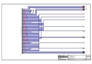
1 Windows CE Stream Interface Driver<br />
All <strong>NetDCU</strong> device drivers are implemented as Windows CE Stream Interface Driver. Thus you can<br />
access these drivers via the File System and the respective File API (CreateFile, WriteFile, ReadFile,<br />
SetFilePointer, <strong>Device</strong>IoControl).<br />
A stream interface driver receives commands from the <strong>Device</strong> Manager and from applications by<br />
means of file system calls. The driver encapsulates all of the information that is necessary to translate<br />
those commands into appropriate actions on the devices that it controls. All stream interface drivers,<br />
whether they manage built-in devices or installable devices, or whether they are loaded at boot time or<br />
loaded dynamically, have similar interactions with other system components. The following illustrations<br />
show the interactions between system components for a generic stream interface driver that manages<br />
a built-in device.<br />
Figure 1: Windows CE: Stream Interface Driver Architecture<br />
Windows CE Stream Interface Driver | 1
2 Analogue Input<br />
Implemented on <strong>NetDCU</strong>: 9,10<br />
<strong>NetDCU</strong> - Windows Embedded CE 6.0<br />
<strong>NetDCU</strong> has 4 analogue inputs. They are internally connected with a resistor (47K) to ground.<br />
This four inputs can be read with this driver. You must install one copy of the driver for each input.<br />
The selection of the channel can be done with the registry key Channel.<br />
Installation of the driver is done by setting some registry values under the following registry key:<br />
[HKLM\<strong>Drivers</strong>\BuiltIn\ANALOGIN]<br />
Required settings:<br />
Key Value Comment<br />
"Prefix" “AIN“ This required value specifies the<br />
driver’s device file name prefix. It is<br />
a three-character identifier, such<br />
as COM.<br />
“Dll“ “ANALOGIN.DLL“ name of the DLL with the driver<br />
“Order“ Dword:0x97 This value specifies the load order<br />
for the driver. If two drivers have<br />
the same load order value, the<br />
drivers load in the order that they<br />
occur in the registry.<br />
“Index“ Dword:1 This value specifies the device<br />
index, a value from 0 through 9.<br />
“Flags” Dword:0 4: Disabeld from loading<br />
“Ioctl“ Dword:4 Call post-initialisation function.<br />
“Channel“ Dword:n Number of the analogue channel.<br />
See Table Channel.<br />
“FriendlyName“ “Analogue input<br />
driver for <strong>NetDCU</strong>“<br />
“Debug” Dword:0|4 Set to 4 to get list of registry<br />
settings at serial debug port.<br />
Default: 0<br />
Table Channel <strong>NetDCU</strong>10:<br />
Table 1: Analogue Input: Registry<br />
Channel Description<br />
0x00 Reads value from analogue input 0 (Connector J7, AD0)<br />
0x01 Reads value from analogue input 1 (Connector J7, AD1)<br />
0x02 Reads value from analogue input 2 (Connector J7, AD2)<br />
0x03 Reads value from analogue input 3 (Connector J7, AD3)<br />
Table 2: Analogue Input: Channels<br />
Analogue Input | 2
Table Channel <strong>NetDCU</strong>9:<br />
Channel Description<br />
0x10 Reads value from analogue input 0 (Connector J7, AD0)<br />
0x14 Reads value from analogue input 1 (Connector J7, AD1)<br />
0x18 Reads value from analogue input 2 (Connector J7, AD2)<br />
0x1C Reads value from analogue input 3 (Connector J7, AD3)<br />
Table 3: Analogue Input: Channels<br />
<strong>NetDCU</strong> - Windows Embedded CE 6.0<br />
Analogue Input | 3
Programming Example:<br />
A. Open one analogue channel:<br />
<strong>NetDCU</strong> - Windows Embedded CE 6.0<br />
HANDLE hAIN;<br />
hAIN = CreateFile( _T("AIN1:"),GENERIC_READ, 0, NULL, OPEN_EXISTING<br />
,FILE_ATTRIBUTE_NORMAL, NULL );<br />
if( hAIN == INVALID_HANDLE_VALUE )<br />
{<br />
ERRORMSG(1,L"Can not open AIN1. LastError = 0x%x\r\n",GetLastError()));<br />
return(FALSE);<br />
}<br />
Listing 1: Analogue Input: Open channel<br />
B. Read data from previously opened channel:<br />
unsigned short data;<br />
DWORD dwSamples = 1;<br />
ReadFile( hAIN, data, dwSamples, &dwSamples, NULL );<br />
if( dwSamples != 1 )<br />
{<br />
ERRORMSG(1,L"Can not read from AIN1. LE = 0x%x\r\n",GetLastError()));<br />
}<br />
Listing 2: Analogue Input: reading samples<br />
C. Select another channel without changing registry:<br />
int nChannel = 0x0;<br />
SetFilePointer( hAIN, nChannel, 0, FILE_BEGIN );<br />
D. Closing the analogue channel:<br />
CloseHandle(hAIN);<br />
Listing 3: Analogue Input: changing channel from application<br />
Listing 4: Analogue Input: closing a channel<br />
Analogue Input | 4
3 Digital I/O<br />
Implemented on <strong>NetDCU</strong>: 9,10<br />
<strong>NetDCU</strong> - Windows Embedded CE 6.0<br />
<strong>NetDCU</strong> has programmable I/O lines at connector J5. You have to use these driver to configure and<br />
access the I/O lines.<br />
Installation of the driver is done by setting some registry values under the following registry key:<br />
[HKLM\<strong>Drivers</strong>\BuiltIn\DIGITALIO]<br />
Required settings:<br />
Key Value Comment<br />
"Prefix" “DIO“ This required value specifies the driver’s<br />
device file name prefix. It is a threecharacter<br />
identifier, such as COM.<br />
“Dll“ “DIGIO.DLL“ Name of the DLL with the driver<br />
“Order“ Dword:0x97 This value specifies the load order for the<br />
driver. If two drivers have the same load<br />
order value, the drivers load in the order<br />
that they occur in the registry.<br />
“Index“ Dword:1 This value specifies the device index, a<br />
value from 0 through 9.<br />
“Ioctl“ Dword:4 Call post-initialisation function.<br />
“Port“ Dword:n 0,1 or 2<br />
UseAsIO Dword:n 1 = The corresponding pin is used as<br />
general purpose I/O.<br />
One bit for each I/O pin.<br />
DataDir Dword:n Data Direction.<br />
0 = The corresponding pin is an input.<br />
1 = The corresponding pin is an output.<br />
One bit for each I/O pin.<br />
DataInit Dword:n Default value of the output pin after driver<br />
initialization.<br />
IRQCfg0 Dword:n Interrupt configuration register 0.<br />
IRQCfg1 Dword:n Interrupt configuration register 1.<br />
IRQCfg2 Dword:n Interrupt configuration register 2.<br />
“FriendlyName“ Digital I/O driver for<br />
<strong>NetDCU</strong>“<br />
“Debug” Dword:0|4 Set to 4 to get list of registry settings at<br />
serial debug port. Default: 0<br />
Table 4: Digital I/O: Registry<br />
Digital I/O | 5
Programming Example:<br />
Headerfile:<br />
#include <br />
A. Opening a digital port<br />
<strong>NetDCU</strong> - Windows Embedded CE 6.0<br />
Listing 5: Digital I/O: Headerfile<br />
HANDLE hDIO = CreateFile(L"DIO1:",GENERIC_READ|GENERIC_WRITE, 0, NULL, OPEN_EXISTING<br />
,FILE_ATTRIBUTE_NORMAL,NULL );<br />
if(INVALID_HANDLE_VALUE == hDIO)<br />
{<br />
ERRORMSG(1,(L"INVALID HANDLE VALUE\r\n"));<br />
return –1;<br />
}<br />
B. Write data to port<br />
unsigned char data = 0xAA;<br />
DWORD dwBytesWrite = 1;<br />
WriteFile( hDIO, &data, dwBytesWrite, &dwBytesWrite, NULL );<br />
if( dwBytesWrite != 1 )<br />
{<br />
ERRORMSG(1,L"Can not write to DIO1. LE = 0x%x\r\n",GetLastError()));<br />
}<br />
C. Change port<br />
LONG lDistance = 1;<br />
SetFilePointer( hDIO, lDistance, NULL, FILE_BEGIN);<br />
D. Get / Set / Clear individual pin<br />
Listing 6: Digital I/O: Open port<br />
Listing 7: Digital I/O: Write port<br />
Listing 8: Digital I/O: Change port<br />
DWORD dwOutCount = 0;<br />
DWORD dwPin = 7;<br />
BYTE byPinLevel = 0xAA;<br />
/*<br />
* Get level of pin.<br />
* dwPin = pin of interest (7 for GPIO7 which is Pin#2 on J5) = input parameter.<br />
* byPinLevel = level of pin = output parameter. 0 = 0V, 1 = 3.3V<br />
*/<br />
<strong>Device</strong>IoControl(g_hDio, IOCTL_DIO_GET_PIN, &dwPin, sizeof(BYTE), &byPinLevel, sizeof(BYTE),<br />
&dwOutCount, NULL);<br />
<strong>Device</strong>IoControl(g_hDio, IOCTL_DIO_SET_PIN, &dwPin, sizeof(BYTE), NULL, 0, &dwOutCount, NULL);<br />
<strong>Device</strong>IoControl(g_hDio, IOCTL_DIO_CLR_PIN, &dwPin, sizeof(BYTE), NULL, 0, &dwOutCount, NULL);<br />
Listing 9: Digital I/O: Access individual pin<br />
E. Request interrupt on J5 pin #2<br />
WAITIRQ cWait; //defined in dio_sdk.h<br />
cWait.bType = FALSE; //set always to false.<br />
cWait.dwTimeOut = 0; //timeout to be blocked (_WAIT_IRQ) by <strong>Device</strong>IoControl.<br />
cWait.dwIOPin = 7; //pin #2 on J5 is GPIO7.<br />
DWORD dwRet=-1;<br />
Digital I/O | 6
<strong>NetDCU</strong> - Windows Embedded CE 6.0<br />
if(!<strong>Device</strong>IoControl(hDIO, IOCTL_DIO_REQUEST_IRQ, &cWait.dwIOPin, sizeof(DWORD), NULL, 0<br />
, &dwRet, NULL))<br />
ERRORMSG(1,(L"IOCTL_DIO_REQUEST_IRQ\r\n"));<br />
Listing 10: Digital I/O: Request interrupt<br />
F. Wait for interrupt<br />
cWait.dwTimeOut = 10000; //timeout (msec) to be blocked by<br />
//<strong>Device</strong>IoControl. INFINITE is possible.<br />
DWORD dwResult=-1; //Result: WAIT_ABANDONED, WAIT_OBJECT_0, WAIT_TIMEOUT.<br />
//For more information see WaitForSingleObject API.<br />
if(!<strong>Device</strong>IoControl(hDIO,IOCTL_DIO_WAIT_IRQ, &cWait, sizeof(WAITIRQ), &dwResult, sizeof(DWORD)<br />
, &dwRet, NULL))<br />
ERRORMSG(1,(L"IOCTL_DIO_WAIT_IRQ\r\n"));<br />
Listing 11: Digital I/O: Wait for interrupt<br />
G. Signal that interrupt processing has been completed<br />
if(!<strong>Device</strong>IoControl(hDIO,IOCTL_DIO_INTDONE_IRQ, &cWait.dwIOPin, sizeof(DWORD), NULL, 0<br />
, &dwRet, NULL))<br />
ERRORMSG(1,(L"IOCTL_DIO_INTDONE_IRQ\r\n"));<br />
Listing 12: Digital I/O: InterruptDone<br />
H. Release interrupt<br />
if(!<strong>Device</strong>IoControl(hDIO,IOCTL_DIO_RELEASE_IRQ, &cWait.dwIOPin, sizeof(DWORD), NULL, 0<br />
, &dwRet, NULL))<br />
ERRORMSG(1,(L"IOCTL_DIO_RELEASE_IRQ\r\n"));<br />
Listing 13: Digital I/O: Release interrupt<br />
I. Closing port<br />
CloseHandle(hDIO);<br />
3.1 Interrupt configuration<br />
Listing 14: Digital I/O: Closing port<br />
IRQCfg2 IRQCfg1 IRQCfg0 Function Note<br />
0 0 0 Interrupt Disabled<br />
0 0 1 Rising Edge Enabled<br />
0 1 0 Falling Edge Enabled<br />
0 1 1 Rising and Falling Edge Enabled<br />
1 0 0 Interrupts Disabled<br />
1 0 1 High Level Enabled Only on <strong>NetDCU</strong>10<br />
1 1 0 Low Level Enabled Only on <strong>NetDCU</strong>10<br />
Table 5: Digital I/O: Interrupt configuration<br />
Digital I/O | 7
3.2 Port description<br />
Port 0:<br />
Port 1:<br />
Port 2:<br />
Bit 7 6 5 4 3 2 1 0<br />
Pin 2 3 4 5 6 7 8 9<br />
R/W R/W R/W R/W R/W R/W R/W R/W R/W<br />
UseAsIO<br />
Bit<br />
7 6 5 4 3 2 1 0<br />
DataDir<br />
Bit<br />
7 6 5 4 3 2 1 0<br />
DataInit<br />
Bit<br />
7 6 5 4 3 2 1 0<br />
IRQCfg0..2 7 6 5 4 3 2 1 0<br />
Table 6: Digital I/O: Port 0<br />
Bit 7 6 5 4 3 2 1 0<br />
Pin --- --- --- --- 10 11 13 15<br />
R/W --- --- --- --- R/W R/W R/W R/W<br />
UseAsIO<br />
Bit<br />
15 14 13 12 11 10 9 8<br />
DataDir<br />
Bit<br />
--- --- --- --- 11 10 9 8<br />
DataInit --- --- --- --- 11 10 9 8<br />
Bit<br />
IRQCfg0..<br />
2<br />
--- --- --- --- --- --- --- ---<br />
Table 7: Digital I/O: Port 1<br />
Bit 7 6 5 4 3 2 1 0<br />
Pin 17 18 19 20 21 22 23 24<br />
R/W R R R R R R R R<br />
UseAsIO<br />
Bit<br />
23 22 21 20 19 18 17 16<br />
DataDir<br />
Bit<br />
--- --- --- --- --- --- --- ---<br />
DataInit --- --- --- --- --- --- --- ---<br />
Bit<br />
IRQCfg0..<br />
2<br />
--- --- --- --- --- --- --- ---<br />
Table 8: Digital I/O: Port 2<br />
<strong>NetDCU</strong> - Windows Embedded CE 6.0<br />
Digital I/O | 8
4 PWM output<br />
Implemented on <strong>NetDCU</strong>: 10<br />
<strong>NetDCU</strong> - Windows Embedded CE 6.0<br />
<strong>NetDCU</strong>10 has 2 PWM outputs. One is controlled by the display driver (contrast voltage) and one can<br />
be controlled by the PWM driver.<br />
Installation of the driver is done by setting some registry values under the following registry key:<br />
[HKLM\<strong>Drivers</strong>\BuiltIn\PWM]<br />
Required settings:<br />
Note:<br />
Key Value Comment<br />
"Prefix" “PWM“ This required value specifies the<br />
driver’s device file name prefix. It is a<br />
three-character identifier, such as<br />
COM.<br />
“Dll“ “ND10_PWM.DLL“ Name of the DLL with the driver<br />
“Order“ Dword:0x97 This value specifies the load order for<br />
the driver. If two drivers have the same<br />
load order value, the drivers load in the<br />
order that they occur in the registry.<br />
“Index“ Dword:1 This value specifies the device index, a<br />
value from 0 through 9.<br />
“Mode” Dword:0|1 0: Absolute mode. Values range<br />
between 0 and “Steps”<br />
1: Percent mode<br />
Values between 0 and 100%.<br />
Default: 1<br />
“Steps” Dword:0..0xFFFF Amount of clocks in one frame.<br />
Default: 0xFFF<br />
“Freq” Dword: Clock frequency<br />
Default: 300000Hz<br />
“FriendlyName“ “PWM driver for<br />
<strong>NetDCU</strong>“<br />
“Debug” Dword:0|4 Set to 4 to get list of registry settings at<br />
serial debug port.<br />
Default: 0<br />
Table 9: PWM: Registy<br />
After opening the channel you can call WriteFile() to set the high phase. Use ReadFile() to read back<br />
the current value. The type of pointer is BYTE for Mode 1 and WORD for Mode 0.<br />
Please take a look at file pwm_sdk.h for additional IOCTL’s.<br />
PWM output | 9
5 LC Display driver<br />
Implemented on <strong>NetDCU</strong>: 9,10<br />
<strong>NetDCU</strong> - Windows Embedded CE 6.0<br />
<strong>NetDCU</strong> has a very flexible and powerful interface for LCD and EL displays. The driver is fully<br />
configurable over the Window CE registry. The user has the possibility to adjust the driver to a new<br />
display by himself.<br />
Registry Key:<br />
<strong>NetDCU</strong> Key<br />
9<br />
[HKLM\<strong>Drivers</strong>\Display\SMIVGX]<br />
10 [HKLM\<strong>Drivers</strong>\Display\SAMSUNG]<br />
Table 10: LCD Driver: Registry path<br />
Use the following parameters to configure the driver:<br />
Key Value Meaning<br />
"Mode" Dword: Number of the predefined configuration<br />
or new user configuration.<br />
“EarlyLCDVoltage” Dword: Set this parameter to 1 power on the<br />
LCD voltage very early at the boot-<br />
process.<br />
Table 11: LCD Driver: Registry<br />
With parameter Mode you have the possibility to use one of the fixed configurations stored in the<br />
kernel or to define a new configuration in registry. Values between 0 and 99 are reserved for fixed<br />
configurations. For your own configuration you have to use values between 100 and 199.<br />
Mode Name Resolution<br />
(wxh)<br />
Type Additional / Desc<br />
0 Kyocera KCS3224 320x240 CSTN <strong>NetDCU</strong>10<br />
1 SHARP LM8V31 640x480 CSTN <strong>NetDCU</strong>10<br />
2 Toshiba LTM04C380K 640x480 TFT <strong>NetDCU</strong>10<br />
3 SHARP LQ104V1DG11 640x480 TFT <strong>NetDCU</strong>10<br />
4 SHARP LQ12S31 800x600 TFT <strong>NetDCU</strong>10<br />
5 SHARP LQ057Q3DC02 320x240 TFT <strong>NetDCU</strong>10<br />
6 Kyocera TCG057 320x240 TFT <strong>NetDCU</strong>10<br />
7 SHARP LQ057V3DG01 640x480 TFT <strong>NetDCU</strong>10<br />
Table 12: LCD Driver: Display modes <strong>NetDCU</strong>10<br />
LC Display driver | 10
<strong>NetDCU</strong> - Windows Embedded CE 6.0<br />
Mode Name Resolution Type Clock Additional / Desc<br />
(wxh)<br />
(MHz)<br />
0 VGA Standard Display 640x480 TFT 25 <strong>NetDCU</strong>9<br />
1 SVGA Standard Display 800x600 TFT 40 <strong>NetDCU</strong>9<br />
2 XGA Standard Display 1024x768 TFT 65 <strong>NetDCU</strong>9<br />
3 SXGA Standard Display 1280x1024 TFT 108 <strong>NetDCU</strong>9<br />
4 QVGA Standard Display 320x240 TFT 6,3 <strong>NetDCU</strong>9<br />
5 XGA Standard Display 1024x768 TFT 56 <strong>NetDCU</strong>9<br />
Table 13: LCD Driver: Display modes <strong>NetDCU</strong>9<br />
For configurations with Mode higher than 99 you have to create a new sub-key with the Name<br />
ModeXXX. Detailed information how to perform these settings and a series of display drivers<br />
adjustments described in the documentation “<strong>NetDCU</strong> Display”.<br />
LC Display driver | 11
6 Matrix-Keyboard<br />
Implemented on <strong>NetDCU</strong>: 9,10<br />
<strong>NetDCU</strong> - Windows Embedded CE 6.0<br />
It is possible to connect a matrix keyboard to <strong>NetDCU</strong>. The organisation of this keyboard is 8 (rows) * 8<br />
(columns) + 4 (static keys). So you can connect 64+4 keys to <strong>NetDCU</strong>. All inputs are internally<br />
connected with resistors to 3.3 Volt. Within the matrix you can only press one key at the same time.<br />
But it is possible to press a matrix key and one or more static keys at the same time. So it is possible<br />
to get the same behaviour as with a PC keyboard. The driver polls the keyboard every 20 ms. In the<br />
case a key is pressed, the driver reads the scan code and saves the value. After additional 20 ms it<br />
checks the scan code. If the scan code is unchanged the scan code will be transformed with the<br />
information stored in the mapping table in a PS2 keyboard scan code. The routing of this keyboard<br />
code is the same as the one from a PS2 keyboard. The mapping table for converting a scan code in an<br />
PS2 keyboard code is stored in the registry.<br />
The settings which influence the driver are stored under key:<br />
[HKLM\HARDWARE\DEVICEMAP\KEYBD\MATRIX]<br />
Key Value Comment<br />
Type Dword:1 Details: Table 15: Matrix Keyboard:<br />
Type / Function<br />
UseAsKey Dword: This values specifies the port pins’s<br />
which are used for keyboard input. See<br />
Table 20: Matrix Keyboard:<br />
Configuration J5 (1) – (3)<br />
RowReverse Dword:0 Reverse all bits of the row. Bit 0 to Bit<br />
7, Bit 1 to Bit6<br />
ColReverse Dword:0 Reverse all bits of the column. Bit 0 to<br />
Bit 7, Bit 1 to Bit6<br />
ChangeRowCol Dword:0 Exchange the scan-value of row and<br />
column.<br />
AutoKeyUp Dword:0 If a matrix key is pressed and the<br />
previous key is not released, this value<br />
sends the KEYUP message to the<br />
system.<br />
OutputScanCode Dword:0 Set this value to 1 to output the scancode<br />
of the currently pressed key as a<br />
debug message on the serial debug<br />
line.<br />
StatKey1 Dword Value for static key 1<br />
StatKey2 Dword Value for static key 2<br />
StatKey3 Dword Value for static key 3<br />
StatKey4 Dword Value for static key 4<br />
Table 14: Matrix Keyboard: Registry<br />
Matrix-Keyboard | 12
<strong>NetDCU</strong> - Windows Embedded CE 6.0<br />
Type Function<br />
0 Matrix keyboard driver OFF<br />
1 Matrix keyboard 8x8+4, 8 rows, 8 cols, 4 static keys, single key detection<br />
3 Matrix keyboard 8x8, 8 rows, 8 cols, 0 static keys, single key detection<br />
17 Matrix keyboard 8x8+4, 8 rows, 8 cols, 4 static keys, multiple key detection<br />
19 Matrix keyboard 8x8, 8 rows, 8 cols, 0 static keys, multiple key detection<br />
Matrix keys are stored under:<br />
Table 15: Matrix Keyboard: Type / Function<br />
[HKLM\HARDWARE\DEVICEMAP\KEYBD\MATRIX\MAP]<br />
Static keys are stored under:<br />
[HKLM\HARDWARE\DEVICEMAP\KEYBD\MATRIX]<br />
Under \MAP you can make settings in the following form:<br />
Key Value<br />
"1" Dword:2<br />
"2" Dword:3<br />
"3" Dword:4<br />
"4" Dword:5<br />
Table 16: Matrix Keyboard: Mapping matrix keys to PS-Codes<br />
The value under Key (string!) is the scan code from the matrix keyboard. The range of this value is<br />
from 1 to 127 and must be given in decimal format. The value must be in hexadecimal form.<br />
In the above example you send the PS2-Code 2 if you press the matrix key 1.<br />
6.1 Default settings<br />
Scan-Code PS2-Code V-Key<br />
0x01 0x02 ‚1‘<br />
0x02 0x03 ‚2‘<br />
0x03 0x04 ‚3‘<br />
0x04 0x05 ‚4‘<br />
0x05 0x06 ‚5‘<br />
0x06 0x07 ‚6‘<br />
0x07 0x08 ‚7‘<br />
0x08 0x09 ‚8‘<br />
0x11 0x0A ‚9‘<br />
0x12 0x0B ‚0‘<br />
0x21 0xE04B VK_LEFT<br />
0x22 0xE04D VK_RIGHT<br />
0x23 0xE048 VK_UP<br />
0x24 0xE050 VK_DOWN<br />
0x25 0x01 VK_ESCAPE<br />
0x26 0x1C VK_RETURN<br />
Table 17: Matrix Keyboard: Default settings<br />
Matrix-Keyboard | 13
6.2 PS2 Scan-Codes<br />
V-KEY PS2-Scan-Code<br />
0 // Scan Code 0x0<br />
VK_ESCAPE // Scan Code 0x1<br />
'1' // Scan Code 0x2<br />
'2' // Scan Code 0x3<br />
'3' // Scan Code 0x4<br />
'4' // Scan Code 0x5<br />
'5' // Scan Code 0x6<br />
'6' // Scan Code 0x7<br />
'7' // Scan Code 0x8<br />
'8' // Scan Code 0x9<br />
'9' // Scan Code 0xA<br />
'0' // Scan Code 0xB<br />
VK_HYPHEN // Scan Code 0xC<br />
VK_EQUAL // Scan Code 0xD<br />
VK_BACK // Scan Code 0xE<br />
VK_TAB // Scan Code 0xF<br />
'Q' // Scan Code 0x10<br />
'W' // Scan Code 0x11<br />
'E' // Scan Code 0x12<br />
'R' // Scan Code 0x13<br />
'T' // Scan Code 0x14<br />
'Y' // Scan Code 0x15<br />
'U' // Scan Code 0x16<br />
'I' // Scan Code 0x17<br />
'O' // Scan Code 0x18<br />
'P' // Scan Code 0x19<br />
VK_LBRACKET // Scan Code 0x1A<br />
VK_RBRACKET // Scan Code 0x1B<br />
VK_RETURN // Scan Code 0x1C<br />
VK_LCONTROL // Scan Code 0x1D<br />
'A' // Scan Code 0x1E<br />
'S' // Scan Code 0x1F<br />
'D' // Scan Code 0x20<br />
'F' // Scan Code 0x21<br />
'G' // Scan Code 0x22<br />
'H' // Scan Code 0x23<br />
'J' // Scan Code 0x24<br />
'K' // Scan Code 0x25<br />
'L' // Scan Code 0x26<br />
VK_SEMICOLON // Scan Code 0x27<br />
VK_APOSTROPH // Scan Code 0x28<br />
VK_BACKQUOTE // Scan Code 0x29<br />
VK_LSHIFT // Scan Code 0x2A<br />
VK_BACKSLASH // Scan Code 0x2B<br />
'Z' // Scan Code 0x2C<br />
'X' // Scan Code 0x2D<br />
'C' // Scan Code 0x2E<br />
'V' // Scan Code 0x2F<br />
'B' // Scan Code 0x30<br />
'N' // Scan Code 0x31<br />
'M' // Scan Code 0x32<br />
VK_COMMA // Scan Code 0x33<br />
<strong>NetDCU</strong> - Windows Embedded CE 6.0<br />
Matrix-Keyboard | 14
VK_PERIOD // Scan Code 0x34<br />
VK_SLASH // Scan Code 0x35<br />
VK_RSHIFT // Scan Code 0x36<br />
VK_MULTIPLY // Scan Code 0x37<br />
VK_LMENU // Scan Code 0x38<br />
VK_SPACE // Scan Code 0x39<br />
VK_CAPITAL // Scan Code 0x3A<br />
VK_F1 // Scan Code 0x3B<br />
VK_F2 // Scan Code 0x3C<br />
VK_F3 // Scan Code 0x3D<br />
VK_F4 // Scan Code 0x3E<br />
VK_F5 // Scan Code 0x3F<br />
VK_F6 // Scan Code 0x40<br />
VK_F7 // Scan Code 0x41<br />
VK_F8 // Scan Code 0x42<br />
VK_F9 // Scan Code 0x43<br />
VK_F10 // Scan Code 0x44<br />
VK_NUMLOCK // Scan Code 0x45<br />
VK_SCROLL // Scan Code 0x46<br />
VK_NUMPAD7 // Scan Code 0x47<br />
VK_NUMPAD8 // Scan Code 0x48<br />
VK_NUMPAD9 // Scan Code 0x49<br />
VK_SUBTRACT // Scan Code 0x4A<br />
VK_NUMPAD4 // Scan Code 0x4B<br />
VK_NUMPAD5 // Scan Code 0x4C<br />
VK_NUMPAD6 // Scan Code 0x4D<br />
VK_ADD // Scan Code 0x4E<br />
VK_NUMPAD1 // Scan Code 0x4F<br />
VK_NUMPAD2 // Scan Code 0x50<br />
VK_NUMPAD3 // Scan Code 0x51<br />
VK_NUMPAD0 // Scan Code 0x52<br />
VK_DECIMAL // Scan Code 0x53<br />
VK_SNAPSHOT // Scan Code 0x54<br />
VK_F11 // Scan Code 0x57<br />
VK_F12 // Scan Code 0x58<br />
VK_LWIN // Scan Code 0x5B<br />
VK_RWIN // Scan Code 0x5C<br />
VK_APPS // Scan Code 0x5D<br />
VK_HELP // Scan Code 0x63<br />
VK_F13 // Scan Code 0x64<br />
VK_F14 // Scan Code 0x65<br />
VK_F15 // Scan Code 0x66<br />
VK_F16 // Scan Code 0x67<br />
VK_F17 // Scan Code 0x68<br />
VK_F18 // Scan Code 0x69<br />
VK_F19 // Scan Code 0x6A<br />
VK_F20 // Scan Code 0x6B<br />
VK_F21 // Scan Code 0x6C<br />
VK_F22 // Scan Code 0x6D<br />
VK_F23 // Scan Code 0x6E<br />
VK_F24 // Scan Code 0x76<br />
VK_DIVIDE // Scan Code 0xE035<br />
VK_SNAPSHOT // Scan Code 0xE037<br />
VK_RMENU // Scan Code 0xE038<br />
VK_HOME // Scan Code 0xE047<br />
VK_UP // Scan Code 0xE048<br />
<strong>NetDCU</strong> - Windows Embedded CE 6.0<br />
Matrix-Keyboard | 15
VK_PRIOR // Scan Code 0xE049<br />
VK_LEFT // Scan Code 0xE04B<br />
VK_RIGHT // Scan Code 0xE04D<br />
VK_END // Scan Code 0xE04F<br />
VK_DOWN // Scan Code 0xE050<br />
VK_NEXT // Scan Code 0xE051<br />
VK_INSERT // Scan Code 0xE052<br />
VK_DELETE // Scan Code 0xE053<br />
VK_LWIN // Scan Code 0xE05B<br />
VK_RWIN // Scan Code 0xE05C<br />
VK_APPS // Scan Code 0xE05D<br />
6.3 Scan-Code Matrix 8x8<br />
Note:<br />
Table 18: Matrix Keyboard: PS2 Scan-Codes<br />
C0 C1 C2 C3<br />
R0 0x01 0x02 0x03 0x04<br />
R1 0x11 0x12 0x13 0x14<br />
R2 0x21 0x22 0x23 0x24<br />
R3 0x31 0x32 0x33 0x34<br />
R4 0x41 0x42 0x43 0x44<br />
R5 0x51 0x52 0x53 0x54<br />
R6 0x61 0x62 0x63 0x64<br />
R7 0x71 0x72 0x73 0x74<br />
C4 C5 C6 C7<br />
R0 0x05 0x06 0x07 0x08<br />
R1 0x15 0x16 0x17 0x18<br />
R2 0x25 0x26 0x27 0x28<br />
R3 0x35 0x36 0x37 0x38<br />
R4 0x45 0x46 0x47 0x48<br />
R5 0x55 0x56 0x57 0x58<br />
R6 0x65 0x66 0x67 0x68<br />
R7 0x75 0x76 0x77 0x78<br />
Table 19: Matrix Keyboard: Scan-Code Matrix 8x8<br />
See see next table for a assignment between R7..R0 and C7..C0 and physical pins.<br />
<strong>NetDCU</strong> - Windows Embedded CE 6.0<br />
Matrix-Keyboard | 16
6.4 Port configuration on J5<br />
Pin 2 3 4 5 6 7 8 9<br />
R/W W W W W W W W W<br />
Meaning R7 R6 R5 R4 R3 R2 R1 R0<br />
UseAsKey<br />
Bit<br />
7 6 5 4 3 2 1 0<br />
Table 20: Matrix Keyboard: Configuration J5 (1)<br />
Pin --- --- --- --- 10 11 13 15<br />
R/W --- --- --- --- R R R R<br />
Meaning C8 C9 C10 C11<br />
UseAsKey<br />
Bit<br />
15 14 13 12 11 10 9 8<br />
Table 21: Matrix Keyboard: Configuration J5 (2)<br />
Pin 17 18 19 20 21 22 23 24<br />
R/W R R R R R R R R<br />
Meaning C7 C6 C5 C4 C3 C2 C1 C0<br />
UseAsKey<br />
Bit<br />
23 22 21 20 19 18 17 16<br />
Table 22: Matrix Keyboard: Configuration J5 (3)<br />
6.5 Matrix Keyboard connector J5<br />
Pin Signal Function Function<br />
ColReverse=0 ColReverse=1<br />
1 ---<br />
2 GPIO7 R7 R7<br />
3 GPIO6 R6 R6<br />
4 GPIO5 R5 R5<br />
5 GPIO4 R4 R4<br />
6 GPIO3 R3 R3<br />
7 GPIO2 R2 R2<br />
8 GPIO1 R1 R1<br />
9 GPIO0 R0 R0<br />
10 GPIO9 StatKey1 StatKey1<br />
11 GPIO10 Statkey2 StatKey2<br />
12 ---<br />
13 GPIO11 StatKey3 StatKey3<br />
14 ---<br />
15 GPIO12 StatKey4 StatKey4<br />
16 GND<br />
17 KBIN0 C7 C0<br />
18 KBIN1 C6 C1<br />
19 KBIN2 C5 C2<br />
20 KBIN3 C4 C3<br />
<strong>NetDCU</strong> - Windows Embedded CE 6.0<br />
Matrix-Keyboard | 17
21 KBIN4 C3 C4<br />
22 KBIN5 C2 C5<br />
23 KBIN6 C1 C6<br />
24 KBIN7 C0 C7<br />
25 VCC<br />
26 VDD<br />
Table 23: Matrix Keyboard: connector J5<br />
<strong>NetDCU</strong> - Windows Embedded CE 6.0<br />
Matrix-Keyboard | 18
7 NANDFMD Driver<br />
Implemented on <strong>NetDCU</strong>: 9,10<br />
[HKLM\<strong>Drivers</strong>\BuiltIn\NandFmd]<br />
Required settings:<br />
<strong>NetDCU</strong> - Windows Embedded CE 6.0<br />
Key Value Comment<br />
"Prefix" “DSK“ This required value specifies the<br />
driver’s device file name prefix. It<br />
is a three-character identifier,<br />
such as COM.<br />
“Dll“ “NANDFMD.DLL“ name of the DLL with the driver<br />
“Order“ Dword:0 This value specifies the load<br />
order for the driver. If two drivers<br />
have the same load order value,<br />
the drivers load in the order that<br />
they occur in the registry.<br />
“Index“ Dword:1 This value specifies the device<br />
index, a value from 0 through 9.<br />
“FriendlyName“ "<strong>NetDCU</strong> flash file system<br />
driver“<br />
“Profile“ “FFSDISK“ Drive name<br />
“FSD” “FATFS.DLL”<br />
Flags Dword:0x1000<br />
Table 24: NANDFMD: Registry<br />
[HKEY_LOCAL_MACHINE\Loader]<br />
"SystemPath"=multi_sz:"\\ffsdisk\\"<br />
Required settings:<br />
Key Value Comment<br />
"SystemPath" multi_sz:"\\ffsdisk\\" Extends the search path to the<br />
folder FFSDISK.<br />
Table 25: NANDFMD: extending the search path<br />
NANDFMD Driver | 19
8 FS-Bus Driver<br />
Implemented on <strong>NetDCU</strong>: 9,10<br />
<strong>NetDCU</strong> - Windows Embedded CE 6.0<br />
This driver is needed to access the parallel extension bus “FS-BUS” at Connector J4. This driver is<br />
also the base driver for all available interfaces for <strong>NetDCU</strong>.<br />
The registry key for the driver is:<br />
[HKLM\<strong>Drivers</strong>\BuiltIn\PARINTF]<br />
Required settings:<br />
Key Value Comment<br />
"Prefix" “PIF“ This required value specifies the driver’s<br />
device file name prefix. It is a threecharacter<br />
identifier, such as COM.<br />
“Dll“ “PARINTF.DLL“ Name of the DLL with the driver.<br />
“Order“ Dword:0x10 This value specifies the load order for the<br />
driver. If two drivers have the same load<br />
order value, the drivers load in the order<br />
that they occur in the registry.<br />
“Index“ Dword:1 This value specifies the device index, a<br />
value from 0 through 9.<br />
“Ioctl“ Dword:4 Call post-initialisation function.<br />
“FriendlyName“ "Parallel interface<br />
driver for <strong>NetDCU</strong>“<br />
“WaitStates” DWORD: Table 27: FS-Bus: Waitstates <strong>NetDCU</strong>9<br />
Table 29: FS-Bus: Waitstates <strong>NetDCU</strong>10<br />
“Debug” DWORD:0 0: no debug output<br />
4: output values read from registry<br />
5: output more debug messages<br />
“IRQ” DWORD: <strong>NetDCU</strong>9: 0x85<br />
<strong>NetDCU</strong>10: 0x21<br />
“IRQCfg” DWORD:2 0=none, 1=raising edge, 2=falling edge<br />
Table 26: FS-Bus: Registry<br />
FS-Bus Driver | 20
8.1 Waitstates <strong>NetDCU</strong>9<br />
<strong>NetDCU</strong> - Windows Embedded CE 6.0<br />
MSCn Bit Description Default<br />
RBUFFx 31 Return Data Buffer vs. Streaming Behavior<br />
When slow memory devices are used in the system (VLIO, slow<br />
SRAM/ROM), this bit must be cleared to allow the system to process<br />
other<br />
information rather than remain idle while all the data is read from the<br />
device. When this bit is cleared, the system is allowed to process other<br />
information. When the bit is set, the system halts and waits until all data<br />
is<br />
returned from the device.<br />
When synchronous static memory devices have been enabled for a given<br />
bank, this bit defaults to streaming behavior. The register bit is read as 0<br />
unless it has specifically been programmed to a 1. This behavior cannot<br />
be overridden.<br />
0 = Slower device (return data buffer)<br />
1 = Faster device (streaming behavior)<br />
0<br />
RRRx [30:28] ROM/SRAM Recovery Time<br />
The value of this bit is half the number of memory clock cycles from the<br />
time that chip select is de-asserted after a read or write until the next chip<br />
select (of a different static memory bank) or nSDCS is asserted.<br />
This field must be programmed with the highest of the three values: tOFF<br />
divided by two, write pulse high time (flash memory/SRAM), and write<br />
recovery before read (flash memory).<br />
tOFF = RRRx * 2 + 1<br />
NOTE: The MSCx[RRR] value (recovery time after chip select<br />
deasserted)<br />
must be reprogrammed prior to switching the processor<br />
to deep-idle mode to avoid long times when the MD<br />
0<br />
RDNx [27:24] ROM Delay Next Access<br />
The RDN field is encoded as follows:<br />
ENCODED (Programmed) Value -----> DECODED (Actual) Value<br />
0-11 -----> 0-11<br />
12 -----> 15<br />
13 -----> 20<br />
14 -----> 26<br />
15 -----> 30<br />
Use the DECODED value in the equations below for RDNx instead of the<br />
actual RDNx value.<br />
For burst ROM or flash memory:<br />
• RDNx + 1 = number of MEM_CLKs from Address to Data Valid for<br />
subsequent access.<br />
For flash memory or SRAM:<br />
• RDNx + 1 = number of CLK_MEMs nWE is asserted for write<br />
accesses<br />
For VLIO:<br />
• RDNx * 2 = amount of time nOE or nPWE is deasserted to address<br />
hold and address setup to nOE or nPWE assertion time.<br />
NOTE: For VLIO, this number must be greater than or equal to 2. The<br />
memory<br />
0<br />
FS-Bus Driver | 21
Note:<br />
<strong>NetDCU</strong> - Windows Embedded CE 6.0<br />
MSCn Bit Description Default<br />
RDFx [23:20] ROM Delay First Access<br />
The encoding scheme is:<br />
ENCODED (programmed) value ------> DECODED (actual) value:<br />
0-11 ------> 0-11<br />
12 ------> 15<br />
13 ------> 20<br />
14 -----> 26<br />
15 ------> 30<br />
The DECODED value represents:<br />
• Number of memory-clock cycles (minus 2) from address to data valid<br />
for first read access from all devices except VLIO<br />
• Number of memory clock cycles (minus 1) from address to data valid<br />
for subsequent read accesses to non-burst devices except VLIO<br />
• Number of memory clock cycles (minus 1) of nWE assertion for write<br />
accesses to all types of flash memory<br />
For variable-latency I/O, this determines the minimum number of memory<br />
clock cycles (minus 1) of nOE (nPWE) assert time for each beat of read<br />
(write).<br />
NOTE: For VLIO, this number must be greater than or equal to 3. The<br />
memory<br />
0<br />
Table 27: FS-Bus: Waitstates <strong>NetDCU</strong>9<br />
Set up the WaitStates value starting at the LSB of the dword (Registry).<br />
Name RBUFFx RRRx RDNx RDFx<br />
Bitpos WaitStates value 11 10 9 8 7 6 5 4 3 2 1 0<br />
Bitpos MSCn 31 30 29 28 27 26 25 24 23 22 21 20<br />
8.2 Waitstates <strong>NetDCU</strong>10<br />
Table 28: FS-Bus: Set up WaitStates value <strong>NetDCU</strong>9<br />
BANKCONn Bit Description Default<br />
Tacs [14:13] Address set-up time before nGCSn<br />
00 = 0 clock 01 = 1 clock<br />
10 = 2 clocks 11 = 4 clocks<br />
00<br />
Tcos [12:11] Chip selection set-up time before nOE<br />
00 = 0 clock 01 = 1 clock<br />
10 = 2 clocks 11 = 4 clocks<br />
00<br />
Tacc [10:8] Access cycle<br />
000 = 1 clock 001 = 2 clocks<br />
010 = 3 clocks 011 = 4 clocks<br />
100 = 6 clocks 101 = 8 clocks<br />
110 = 10 clocks 111 = 14 clocks<br />
Note: When nWAIT signal is used, Tacc >= 4<br />
clocks.<br />
111<br />
FS-Bus Driver | 22
<strong>NetDCU</strong> - Windows Embedded CE 6.0<br />
BANKCONn Bit Description Default<br />
Tcoh [7:6] Chip selection hold time after nOE<br />
00 = 0 clock 01 = 1 clock<br />
10 = 2 clocks 11 = 4 clocks<br />
000<br />
Tcah [5:4] Address hold time after nGCSn<br />
00 = 0 clock 01 = 1 clock<br />
10 = 2 clocks 11 = 4 clocks<br />
Programming Example:<br />
Headerfile:<br />
#include <br />
A. Opening FS-Bus handle<br />
Table 29: FS-Bus: Waitstates <strong>NetDCU</strong>10<br />
HANDLE hPIF = CreateFile(L"PIF1:",GENERIC_WRITE, 0, NULL, OPEN_EXISTING<br />
,FILE_ATTRIBUTE_NORMAL,NULL );<br />
if(INVALID_HANDLE_VALUE == hPIF)<br />
{<br />
ERRORMSG(1,(L"INVALID HANDLE VALUE\r\n"));<br />
return –1;<br />
}<br />
B. Write data without address<br />
00<br />
Listing 15: FS-Bus: Headerfile<br />
Listing 16: FS-Bus: Opening handle<br />
unsigned char data[3] = { 0x1, 0x2, 0x3 };<br />
DWORD dwBytesWrite = 1;<br />
WriteFile( hDIO, data, 3, &dwBytesWrite, NULL );<br />
if( dwBytesWrite != 3 )<br />
{<br />
ERRORMSG(1,L"Can not write to PIF1. LE = 0x%x\r\n",GetLastError()));<br />
}<br />
Listing 17: FS-Bus: Write data without address<br />
C. Read data without address<br />
unsigned char data[3] = { 0x1, 0x2, 0x3 };<br />
DWORD dwRead;<br />
ReadFile( hDIO, data, 3, &dwRead, NULL );<br />
if( dwRead != 3 )<br />
{<br />
ERRORMSG(1,L"Can not read from PIF1. LE = 0x%x\r\n",GetLastError()));<br />
}<br />
Listing 18: FS-Bus: Read data without address<br />
D. Write address / data to bus<br />
PARINTFRW cData;<br />
DWORD dwBytesReturend;<br />
cData.chAddress = 0x20;<br />
FS-Bus Driver | 23
<strong>NetDCU</strong> - Windows Embedded CE 6.0<br />
if( !<strong>Device</strong>IoControl( m_hPIF,<br />
IOCTL_PARINTF_WRITE,<br />
&cData, sizeof(cData), NULL, 0,<br />
&dwBytesReturend, NULL ) )<br />
{<br />
ERRORMSG(1,L"Can not write to PIF1. LE = 0x%x\r\n",GetLastError()));<br />
}<br />
Listing 19: FS-Bus: Write address / data to bus<br />
E. Read one byte from bus<br />
PARINTFRW cData;<br />
DWORD dwBytesReturend;<br />
cData.chAddress = 0x20;<br />
cData.chData = 1;<br />
if( !<strong>Device</strong>IoControl( m_hPIF,<br />
IOCTL_PARINTF_READ,<br />
&cData, sizeof(cData), NULL, 0,<br />
&dwBytesReturend, NULL ) )<br />
{<br />
ERRORMSG(1,L"Can not read from PIF1. LE = 0x%x\r\n",GetLastError()));<br />
}<br />
Listing 20: FS-Bus: Read one byte from bus<br />
F. Handle interrupt<br />
DWORD dwTimeOut = 30000; //Timeout to be blocked by _WAIT_IRQ (<strong>Device</strong>IoControl).<br />
DWORD dwWaitRes = -1; //Return value that indicates the event result.<br />
//WAIT_OBJECT_0,WAIT_ABANDONED,WAIT_TIMEOUT.<br />
//For more information see WaitForSingleObject API.<br />
DWORD dwBytesReturend = -1;<br />
//Wait for interrupt<br />
<strong>Device</strong>IoControl( hPIF,IOCTL_PARINTF_WAIT_IRQ, &dwTimeOut, sizeof(DWORD)<br />
, &dwWaitRes, sizeof(DWORD)<br />
, &dwBytesReturend, NULL );<br />
//Call InterruptDone<br />
<strong>Device</strong>IoControl( hPIF,IOCTL_PARINTF_DONE_IRQ, NULL, sizeof(DWORD), NULL, sizeof(DWORD)<br />
, &dwBytesReturend, NULL );<br />
Listing 21: FS-Bus: Handling interrupt<br />
FS-Bus Driver | 24
9 Serial Driver<br />
Implemented on <strong>NetDCU</strong>: 9,10<br />
This driver is needed to access the serial interfaces COM1:, COM2: and COM3:.<br />
The registry key for the driver is:<br />
[HKLM\<strong>Drivers</strong>\BuiltIn\SERIAL1]<br />
[HKLM\<strong>Drivers</strong>\BuiltIn\SERIAL2]<br />
[HKLM\<strong>Drivers</strong>\BuiltIn\SERIAL3]<br />
Optional settings:<br />
RS485 Mode<br />
<strong>NetDCU</strong> - Windows Embedded CE 6.0<br />
Key Value Comment<br />
"Priority256" Dword:104 Priority for serial receive/transmit thread.<br />
Default: 104<br />
“WaterMarker“ Dword:1,8,16,32 FIFO trigger level.<br />
Default: 8<br />
RS485 Dword: Enable RS485 mode for COM2:<br />
Default: 0<br />
(<strong>NetDCU</strong>10)<br />
With <strong>NetDCU</strong>10 you can toggle COM2: between RS232 and RS485. To do this, you have to add<br />
registry value RS485 and set it to 1. Additionally you have to modify DCB in the way that<br />
dcb.fRtsControl is equal to RTS_CONTROL_TOGGLE.<br />
Programming Example:<br />
DCB dcb;<br />
dcb.DCBlength = sizeof( dcb );<br />
GetCommState( g_hCOM, &dcb );<br />
dcb.ByteSize = 8;<br />
dcb.Parity = NOPARITY;<br />
dcb.StopBits = ONESTOPBIT;<br />
dcb.BaudRate = CBR_38400;<br />
dcb.fOutxCtsFlow = 0;<br />
dcb.fRtsControl = RTS_CONTROL_TOGGLE;<br />
SetCommState( g_hCOM, &dcb );<br />
Listing 22: Serial: Using COM2 in RS485 mode (<strong>NetDCU</strong>10)<br />
Serial Driver | 25
10 Driver for NDCU-ADP/UART<br />
Implemented on <strong>NetDCU</strong>: 9,10<br />
<strong>NetDCU</strong> - Windows Embedded CE 6.0<br />
<strong>NetDCU</strong> has 3 integrated serial lines. If more serial lines or a serial line with all modem signals or a<br />
RS422/485 is needed you can use the extension board NDCU-ADP/UART to get two more serial lines.<br />
For hardware documentation take a look at document “UART-Adapter”.<br />
This driver can only work if the driver PARINTF is installed and running. Check this under<br />
\HKLM\<strong>Drivers</strong>\Active.<br />
Installation of the driver is done by setting some registry values under the following registry key:<br />
[HKLM\<strong>Drivers</strong>\BuiltIn\SERIAL3]<br />
[HKLM\<strong>Drivers</strong>\BuiltIn\SERIAL4]<br />
Key Value Comment<br />
"Prefix" “COM“ This required value specifies the driver’s<br />
device file name prefix. It is a threecharacter<br />
identifier, such as COM.<br />
“Dll“ “UARTINTF.DLL“ Name of the DLL with the driver.<br />
“Order“ Dword:35<br />
Dword:36<br />
This value specifies the load order for the<br />
driver. If two drivers have the same load<br />
order value, the drivers load in the order<br />
that they occur in the registry.<br />
“Index“ Dword:3 This value specifies the device index, a<br />
Dword:4 value from 0 through 9.<br />
“Ioctl“ Dword:4 Call post-initialisation function.<br />
“Port“ “PIF1:” This value specifies the device name of<br />
<strong>Device</strong>ArrayIndex Dword:0<br />
Dword:1<br />
that parallel port. Normally this is PIF1:.<br />
Number of the hardware port you want to<br />
access.<br />
0:Port at connector J1<br />
1: Port at connector J2<br />
RcvrTriggerLevel Dword:8 The UART on the NDCU-ADP/UART has<br />
a 16 byte receive FIFO. With this value<br />
you can setup the trigger level for the<br />
receive interrupt.<br />
Priority256 Dword:103 Priority for this thread.<br />
“FriendlyName“ “Serial driver for<br />
<strong>NetDCU</strong>“<br />
Table 30: Registry: NDCU-ADP/UART<br />
Driver for NDCU-ADP/UART | 26
11 Driver for NDCU-ADP/CAN2<br />
Implemented on <strong>NetDCU</strong>: 9,10<br />
<strong>NetDCU</strong> - Windows Embedded CE 6.0<br />
The connectivity of <strong>NetDCU</strong> could be significantly enhanced with 2 CAN lines by usage of NDCU-<br />
ADP/CAN2. For hardware documentation take a look at document “CAN-Adapter”. This document only<br />
describes the installation of the driver. The usage of the driver is described in document “WINCE-CAN-<br />
Interface”<br />
This driver can only work if the driver PARINTF is installed and running. Check this under<br />
\HKLM\<strong>Drivers</strong>\Active.<br />
Installation of the driver is done by setting some registry values under the following registry key:<br />
[HKLM\<strong>Drivers</strong>\BuiltIn\CAN1]<br />
[HKLM\<strong>Drivers</strong>\BuiltIn\CAN2]<br />
Key Value Comment<br />
Prefix “CID“ This required value specifies the driver’s<br />
device file name prefix. It is a three-character<br />
identifier, such as COM.<br />
Dll “CANINTF.DLL“ Name of the DLL with the driver.<br />
Order Dword:75<br />
Dword:76<br />
This value specifies the load order for the<br />
driver. If two drivers have the same load<br />
order value, the drivers load in the order that<br />
they occur in the registry.<br />
Index Dword:0 This value specifies the device index, a value<br />
Dword:1 from 0 through 9.<br />
Ioctl Dword:4 Call post-initialisation function.<br />
Port “PIF1:” This value specifies the device name of the<br />
<strong>Device</strong>ArrayIndex Dword:0<br />
Dword:1<br />
parallel port. Normally this is PIF1:.<br />
Number of the hardware port you want to<br />
access.<br />
0:Port at connector J3<br />
1: Port at connector J4<br />
Priority256 Dword:103 Priority for this thread.<br />
FriendlyName “CAN driver for<br />
<strong>NetDCU</strong>“<br />
Baudrate Dword:1000000<br />
Virtualize Dword:0<br />
“Debug” Dword:0|4 Set to 4 to get list of registry settings at serial<br />
debug port.<br />
Default: 0<br />
Table 31: Registry: NDCU-ADP/CAN2<br />
Driver for NDCU-ADP/CAN2 | 27
12 Touchpanel Driver<br />
Implemeted on <strong>NetDCU</strong>: 9,10<br />
[HKEY_LOCAL_MACHINE\HARDWARE\DEVICEMAP\TOUCH]<br />
<strong>NetDCU</strong> - Windows Embedded CE 6.0<br />
Key Value Comment<br />
"CalibrationData" “0,0,0,0,0,” Set this value to the given string to<br />
avoid the calibration screen after<br />
restart.<br />
“TouchSamples” Dword:3..20 With this value you can adjust the<br />
amount of samples that are used to<br />
create the position value. As more<br />
samples as longer the time you have<br />
to press on the same place.<br />
Default: 7<br />
“DeltaXCoordTolerance” Dword:0..0x3FF This value is used by the touch<br />
sample filter routine to accept and<br />
reject points. Increasing the<br />
tolerance will generally allow faster<br />
pen movements to be detected.<br />
This will also increase noise and<br />
tend to cause erratic touch<br />
behaviour.<br />
Default: 20<br />
“DeltaYCoordTolerance” Dword:0..0x3FF This value is used by the touch<br />
sample filter routine to accept and<br />
reject points. Increasing the<br />
tolerance will generally allow faster<br />
pen movements to be detected.<br />
This will also increase noise and<br />
tend to cause erratic touch<br />
behaviour.<br />
Default: 16<br />
MinMove Dword:1..0x3FF Minimum move (A/D resolution)<br />
before MouseMove is signalled.<br />
MinMove: 5<br />
MaxMove Dword:1..0x3FF Maximum move (A/D resolution)<br />
which is recognized and send to<br />
application layer.<br />
MaxMove: 50<br />
AutoCalib Dword:0..10000 Time in ms before event 20 is<br />
signalled to application layer when<br />
touch is pressed. Can be used for<br />
automatic touch calibration.<br />
AutoCalib=0 disables this function.<br />
Default: 0<br />
“Debug” Dword:0|4 Set to 4 to get list of registry settings<br />
at serial debug port.<br />
Default: 0<br />
Table 32: Touch: Registry<br />
Touchpanel Driver | 28
[HKEY_LOCAL_MACHINE\SYSTEM\CALIBRUI]<br />
Possible settings:<br />
<strong>NetDCU</strong> - Windows Embedded CE 6.0<br />
Key Value Comment<br />
"NoKeyboard" Dword:1 This parameter tells touch panel calibration to not wait for<br />
a keystroke at the end of calibration.<br />
Table 33: Touch: CALIBRUI<br />
[HKEY_LOCAL_MACHINE\HARDWARE\DEVICEMAP\TOUCH]<br />
Possible settings:<br />
Key Value Comment<br />
"Priority256"<br />
”HighPriority256“<br />
Dword:109 Set this value to adjust the priority of the touch panel<br />
driver.<br />
Table 34: Touch: Adjust priority<br />
Touchpanel Driver | 29
13 USB Mass Storage Class Driver<br />
Implemented on <strong>NetDCU</strong>: 9,10<br />
<strong>NetDCU</strong> - Windows Embedded CE 6.0<br />
[HKEY_LOCAL_MACHINE\<strong>Drivers</strong>\USB\Client<strong>Drivers</strong>\Mass_Storage_Class\6]<br />
Possible settings:<br />
Key Value Comment<br />
"Prefix" “DSK“ This required value specifies the<br />
driver’s device file name prefix. It is a<br />
three-character identifier, such as<br />
COM.<br />
“Dll“ “USBDISK6.DLL“ name of the DLL with the driver<br />
“Folder“ “USB Disk”<br />
“Ioctl“ Dword:4 Call post-initialisation function.<br />
“FSD” “FATFS.DLL”<br />
“DisableModeSense10” DWORD:0 Disable the call to the function which<br />
detects the device mode.<br />
Necessary for some USB memory<br />
adaptors.<br />
Table 35: USB Maß Storage: Registry<br />
USB Mass Storage Class Driver | 30
14 Soft-Keyboard<br />
Implemented on <strong>NetDCU</strong>: 9,10<br />
<strong>NetDCU</strong> - Windows Embedded CE 6.0<br />
Sometimes it is useful to have a virtual keyboard on your display which can be controlled by using the<br />
touch panel.<br />
The configuration program NDCUCFG (version 012 and higher) has a command to show the input<br />
panel on the screen (sip on).<br />
Installation of the driver softkb.dll is done by setting some registry values under the following registry<br />
key:<br />
[HKEY_LOCAL_MACHINE\<strong>Drivers</strong>\BuiltIn\SIP]<br />
Required settings:<br />
Key Value Comment<br />
"Prefix" “SIP“ This required value specifies the driver’s device file<br />
name prefix. It is a three-character identifier, such as<br />
COM.<br />
“Dll“ “SOFTKB.DLL“ name of the driver file<br />
“Order“ Dword:1 This value specifies the load order for the driver. If two<br />
drivers have the same load order value, the drivers<br />
load in the order that they occur in the registry.<br />
“Index“ Dword:0 This value specifies the device index, a value from 0<br />
through 9.<br />
Flags Dword:0x10<br />
Table 36: SIP: Registry<br />
Soft-Keyboard | 31
15 Audio Driver<br />
Implemented on <strong>NetDCU</strong>: 10<br />
<strong>NetDCU</strong> - Windows Embedded CE 6.0<br />
Audio driver for <strong>NetDCU</strong> is implemented as wavdev2 driver and can be configured under the following<br />
registry key:<br />
[HKEY_LOCAL_MACHINE\<strong>Drivers</strong>\BuiltIn\Audio]<br />
Possible settings:<br />
Key Value Comment<br />
“Prefix” “WAV” This required value specifies the driver’s<br />
device file name prefix. It is a threecharacter<br />
identifier, such as COM.<br />
“DLL” “wavedev_n10.dll” name of the driver file<br />
“Order” Dword:0x20<br />
“Index” Dword:1 This value specifies the device index, a<br />
value from 0 through 9.<br />
“InChannel” Dword:n This value selects the input channel.<br />
2 = Line-In<br />
3 = Microphone<br />
“MicBoost” Dword:0|1 Set this 1 to boost microphone input by<br />
20dB.<br />
Default: 0<br />
“LineInOutBypass” Dword:0|1 Set this to 1 to route Line-In directly to<br />
Line-Out.<br />
Default: 0<br />
“LineInVolLeft” Dword:n Volume for Line-In left.<br />
Default: 0x17<br />
“LineInVolRight” Dword:n Volume for Line-In right.<br />
Default: 0x17<br />
“Debug” Dword:0|4 Set to 4 to get list of registry settings at<br />
serial debug port.<br />
Default: 0<br />
Table 37: Audio: Registry<br />
Soft-Keyboard | 32
16 NDCUCFG<br />
Implemented on <strong>NetDCU</strong>: all<br />
<strong>NetDCU</strong> - Windows Embedded CE 6.0<br />
This utility is always included in the Windows CE image and enables the customer to access the<br />
registry from the command line and to call some additional helper functions.<br />
Ndcucfg.exe can be started over serial, telnet or from within a command window.<br />
By default, ndcucfg.exe is started from a Launch/Depend configuration in<br />
[HKEY_LOCAL_MACHINE\Init]<br />
and receives commands over serial line COM1:. If you want to change the serial line you can find<br />
settings of ndcucfg.exe under the following registry key:<br />
[HKEY_LOCAL_MACHINE\System\NDCUCFG]<br />
Possible settings:<br />
Key Value Comment<br />
"Port" “COM1:” NDCUFG is automatically started during boot because<br />
of a entry in HKLM\INIT.<br />
With this value you can specify on which serial line<br />
ndcucfg uses for communication.<br />
"BatchFile“ String The commands in the file will be executed during start of<br />
ndcucfg.exe.<br />
List of commands (not complete):<br />
Table 38: NDCUCFG: Registry<br />
- display mode set <br />
Changes the display mode to the given number.<br />
- display mode get<br />
Retrieves the display mode.<br />
- display rotate get<br />
Retrieves the display rotation angle.<br />
- display rotate set <br />
Changes the display rotation to the given angle.<br />
- reg open<br />
opens the root key under HKLM<br />
- reg open <br />
opens the specified key under HKLM(open)<br />
- reg opencu <br />
opens the specified key under HKCU(opencu)<br />
- reg enum<br />
displays a list of all keys and values under the current<br />
location<br />
- reg set value dword <br />
- reg set value string <br />
NDCUCFG | 33
- reg set value multi ;<br />
- reg set value hex ,,<br />
sets/creates the value with name to the value<br />
<br />
- reg create key <br />
Creates the specified sub-key and opens it.<br />
- reg del value <br />
Delete the specified value from registry.<br />
- reg del key <br />
Delete the specified key from registry.<br />
- reg save<br />
Saves the registry in flash memory, so that modifications<br />
are available after reset.<br />
- fat format <br />
Formats the volume with name .<br />
- contrast +<br />
Increase contrast voltage of LCD (small steps)<br />
- contrast ++<br />
Increase contrast voltage of LCD (large steps)<br />
- contrast -<br />
Decrease contrast voltage of LCD (small steps)<br />
- contrast --<br />
Decrease contrast voltage of LCD (large steps)<br />
- contrast get<br />
Returns the current contrast voltage of LCD.<br />
- contrast set <br />
Sets the contrast voltage of LCD. The value is the high time<br />
for the PWM circuit.<br />
- backlight on<br />
Switch on backlight of LCD<br />
- backlight off<br />
Switch off backlight of LCD<br />
- touch calibrate<br />
Shows the calibration screen for the touch panel.<br />
- sip on<br />
Shows the input panel window.<br />
- sip off<br />
Hides the input panel window.<br />
- reboot<br />
Reboots the device.<br />
- cert import cert <br />
Import certificate with filename into certificate store<br />
. Values for MY, CA or ROOT<br />
- cert import pkey <br />
Import private key from file into certificate store MY, CA or<br />
ROOT<br />
- cert enum<br />
List all certificates from store MY, CA and ROOT<br />
- cert delete <br />
Delete certificate<br />
- user create <br />
Creates new use with password<br />
- user delete <br />
Delete user<br />
- user enum<br />
List all users<br />
- REM <br />
Records comments (remarks) in a batch file.<br />
<strong>NetDCU</strong> - Windows Embedded CE 6.0<br />
NDCUCFG | 34
- ECHO <br />
Displays messages.<br />
- start <br />
Creates a new process and its primary thread.<br />
- ndcucfg -B<br />
runs as batch process.<br />
<strong>NetDCU</strong> - Windows Embedded CE 6.0<br />
NDCUCFG | 35
17 Extending the Search Path<br />
Implemented on: all<br />
<strong>NetDCU</strong> - Windows Embedded CE 6.0<br />
It’s possible to extend the default path that the kernel uses to locate executable files. The necessary<br />
entry can be found under registry key:<br />
HKEY_LOCAL_MACHINE\Loader<br />
Possible settings:<br />
Key Value Comment<br />
"SystemPath" Multi:“\\ffsdisk\\” To extend the path you must add values to<br />
the value.<br />
Table 39: Ext. Search Path<br />
Extending the Search Path | 36
18 Module FATUI<br />
<strong>NetDCU</strong> - Windows Embedded CE 6.0<br />
This module implements the user interface for the FAT file system. This module is used if the file<br />
system must show a dialog box to interact with the user. This happens for example if the user inserts a<br />
PCMCIA card or the file system detects an unformatted drive.<br />
In general dialog boxes are a good idea. But if the user has not connected a display to device all kind<br />
of display output is unusable. Because of that we have added an option to redirect all display output to<br />
the serial line at connector ST6. The value can be found under key:<br />
[HKLM\System\FATUI]<br />
Parameter:<br />
Key Value Meaning<br />
"AutoAnswer" Dword:0|1 Set this value to 1 to redirect all output to serial line at<br />
connector ST6. The question to format the drive will<br />
be automatically answered with YES, all other<br />
questions will be answered with FATUI_NONE.<br />
Table 40: FATUI: redirect output to serial line<br />
Module FATUI | 37
19 Module NETUI<br />
<strong>NetDCU</strong> - Windows Embedded CE 6.0<br />
This module implements the user interface for the Network access. This module is used if a network<br />
resource is accessed which needs a user and password. By setting the described parameters, it is<br />
possible to avoid the normally shown dialog box.<br />
The value can be found under key:<br />
[HKLM\System\NETUI]<br />
Parameter:<br />
Key Value Meaning<br />
"AutoLogon" Dword:0|1 Set this value to 1 to use the registry values<br />
UserName and Password for network access.<br />
"UserName“ String<br />
"Password“ String<br />
Table 41: NETUI: AutoLogon<br />
Module NETUI | 38
20 Appendix<br />
Important Notice<br />
The information in this publication has been carefully checked and is believed to be entirely accurate at<br />
the time of publication. F&S <strong>Elektronik</strong> <strong>Systeme</strong> assumes no responsibility, however, for possible<br />
errors or omissions, or for any consequences resulting from the use of the information contained in this<br />
documentation.<br />
F&S <strong>Elektronik</strong> <strong>Systeme</strong> reserves the right to make changes in its products or product specifications or<br />
product documentation with the intent to improve function or design at any time and without notice and<br />
is not required to update this documentation to reflect such changes.<br />
F&S <strong>Elektronik</strong> <strong>Systeme</strong> makes no warranty or guarantee regarding the suitability of its products for<br />
any particular purpose, nor does F&S <strong>Elektronik</strong> <strong>Systeme</strong> assume any liability arising out of the<br />
documentation or use of any product and specifically disclaims any and all liability, including without<br />
limitation any consequential or incidental damages.<br />
Products are not designed, intended, or authorized for use as components in systems intended for<br />
applications intended to support or sustain life, or for any other application in which the failure of the<br />
product from F&S <strong>Elektronik</strong> <strong>Systeme</strong> could create a situation where personal injury or death may<br />
occur. Should the Buyer purchase or use a F&S <strong>Elektronik</strong> <strong>Systeme</strong> product for any such unintended<br />
or unauthorized application, the Buyer shall indemnify and hold F&S <strong>Elektronik</strong> <strong>Systeme</strong> and its<br />
officers, employees, subsidiaries, affiliates, and distributors harmless against all claims, costs,<br />
damages, expenses, and reasonable attorney fees arising out of, either directly or indirectly, any claim<br />
of personal injury or death that may be associated with such unintended or unauthorized use, even if<br />
such claim alleges that F&S <strong>Elektronik</strong> <strong>Systeme</strong> was negligent regarding the design or manufacture of<br />
said product.<br />
Appendix | 39
Listings<br />
Listing 1: Analogue Input: Open channel................................................................................................. 4<br />
Listing 2: Analogue Input: reading samples............................................................................................. 4<br />
Listing 3: Analogue Input: changing channel from application................................................................. 4<br />
Listing 4: Analogue Input: closing a channel ........................................................................................... 4<br />
Listing 5: Digital I/O: Headerfile ............................................................................................................... 6<br />
Listing 6: Digital I/O: Open port................................................................................................................ 6<br />
Listing 7: Digital I/O: Write port................................................................................................................ 6<br />
Listing 8: Digital I/O: Change port............................................................................................................ 6<br />
Listing 9: Digital I/O: Request interrupt .................................................................................................... 7<br />
Listing 10: Digital I/O: Wait for interrupt................................................................................................... 7<br />
Listing 11: Digital I/O: InterruptDone........................................................................................................ 7<br />
Listing 12: Digital I/O: Release interrupt .................................................................................................. 7<br />
Listing 13: Digital I/O: Closing port .......................................................................................................... 7<br />
Listing 14: FS-Bus: Headerfile............................................................................................................... 23<br />
Listing 15: FS-Bus: Opening handle ...................................................................................................... 23<br />
Listing 16: FS-Bus: Write data without address..................................................................................... 23<br />
Listing 17: FS-Bus: Read data without address..................................................................................... 23<br />
Listing 18: FS-Bus: Write address / data to bus .................................................................................... 24<br />
Listing 19: FS-Bus: Read one byte from bus......................................................................................... 24<br />
Listing 20: FS-Bus: Handling interrupt ................................................................................................... 24<br />
Listing 21: Serial: Using COM2 in RS485 mode (<strong>NetDCU</strong>10)............................................................... 25<br />
Figures<br />
Figure 1: Windows CE: Stream Interface Driver Architecture ................................................................. 1<br />
Tables<br />
Table 1: Analogue Input: Registry ........................................................................................................... 2<br />
Table 2: Analogue Input: Channels ......................................................................................................... 2<br />
Table 3: Analogue Input: Channels ......................................................................................................... 3<br />
Table 4: Digital I/O: Registry.................................................................................................................... 5<br />
Table 5: Digital I/O: Interrupt configuration.............................................................................................. 7<br />
Table 6: Digital I/O: Port 0 ....................................................................................................................... 8<br />
Table 7: Digital I/O: Port 1 ....................................................................................................................... 8<br />
Table 8: Digital I/O: Port 2 ....................................................................................................................... 8<br />
Table 9: PWM: Registy............................................................................................................................ 9<br />
Table 10: LCD Driver: Registry path...................................................................................................... 10<br />
Table 11: LCD Driver: Registry.............................................................................................................. 10<br />
Table 12: LCD Driver: Display modes <strong>NetDCU</strong>10................................................................................. 10<br />
Table 13: LCD Driver: Display modes <strong>NetDCU</strong>9................................................................................... 11<br />
Table 14: Matrix Keyboard: Registry...................................................................................................... 12<br />
Table 15: Matrix Keyboard: Type / Function.......................................................................................... 13<br />
Table 16: Matrix Keyboard: Mapping matrix keys to PS-Codes ............................................................ 13<br />
Table 17: Matrix Keyboard: Default settings.......................................................................................... 13<br />
Table 18: Matrix Keyboard: PS2 Scan-Codes ....................................................................................... 16<br />
Table 19: Matrix Keyboard: Scan-Code Matrix 8x8............................................................................... 16<br />
Table 20: Matrix Keyboard: Configuration J5 (1) ................................................................................... 17<br />
Table 21: Matrix Keyboard: Configuration J5 (2) ................................................................................... 17<br />
Appendix | 40
Table 22: Matrix Keyboard: Configuration J5 (3) ................................................................................... 17<br />
Table 23: Matrix Keyboard: connector J5.............................................................................................. 18<br />
Table 24: NANDFMD: Registry.............................................................................................................. 19<br />
Table 25: NANDFMD: extending the search path ................................................................................. 19<br />
Table 26: FS-Bus: Registry.................................................................................................................... 20<br />
Table 27: FS-Bus: Waitstates <strong>NetDCU</strong>9 ............................................................................................... 22<br />
Table 28: FS-Bus: Set up WaitStates value <strong>NetDCU</strong>9.......................................................................... 22<br />
Table 29: FS-Bus: Waitstates <strong>NetDCU</strong>10 ............................................................................................. 23<br />
Table 30: Registry: NDCU-ADP/UART.................................................................................................. 26<br />
Table 31: Registry: NDCU-ADP/CAN2 .................................................................................................. 27<br />
Table 32: Touch: Registry...................................................................................................................... 28<br />
Table 33: Touch: CALIBRUI .................................................................................................................. 29<br />
Table 34: Touch: Adjust priority............................................................................................................. 29<br />
Table 35: USB Maß Storage: Registry .................................................................................................. 30<br />
Table 36: SIP: Registry.......................................................................................................................... 31<br />
Table 37: Audio: Registry ...................................................................................................................... 32<br />
Table 38: NDCUCFG: Registry.............................................................................................................. 33<br />
Table 39: Ext. Search Path.................................................................................................................... 36<br />
Table 40: FATUI: redirect output to serial line ....................................................................................... 37<br />
Table 41: NETUI: AutoLogon................................................................................................................. 38<br />
Appendix | 41