NetDCU/ADP-TCG057-L - F&S Elektronik Systeme GmbH.
NetDCU/ADP-TCG057-L - F&S Elektronik Systeme GmbH.
NetDCU/ADP-TCG057-L - F&S Elektronik Systeme GmbH.

Create successful ePaper yourself
Turn your PDF publications into a flip-book with our unique Google optimized e-Paper software.
<strong>NetDCU</strong>/<strong>ADP</strong>-<strong>TCG057</strong>-L<br />
<strong>NetDCU</strong>x<br />
Version 1.01 Date 01.08.2008<br />
© by F&S <strong>Elektronik</strong> <strong>Systeme</strong> <strong>GmbH</strong> 2008<br />
F&S <strong>Elektronik</strong> <strong>Systeme</strong> <strong>GmbH</strong><br />
Untere Waldplätze 23<br />
D-70569 Stuttgart<br />
Phone: +49-711-123722-0 Fax: +49-711-123722-99
Table of Contents<br />
1 Description ..............................................................1<br />
2 Connectors and Configuration...............................2<br />
3 Connectors..............................................................3<br />
3.1 J1 <strong>NetDCU</strong> Interface .................................................3<br />
4 Configuration <strong>NetDCU</strong>/<strong>ADP</strong>-<strong>TCG057</strong>-L...................5<br />
4.1 Configuration Display Interface Pin 30.......................7<br />
4.2 Configuration Display Interface Pin 31.......................7<br />
5 Dimensions <strong>NetDCU</strong>/<strong>ADP</strong>-<strong>TCG057</strong>-L......................8
1 Description<br />
The <strong>NetDCU</strong>/<strong>ADP</strong>-<strong>TCG057</strong>-L is used to connect the Kyocera<br />
<strong>TCG057</strong> display series with LED backlight to the starterkit of<br />
<strong>NetDCU</strong> and PicoMOD family.<br />
This display Adapter to support <strong>TCG057</strong>QVLBA and<br />
<strong>TCG057</strong>VGLBA from Kyocera.<br />
It has three software adjustable 15mA current sources for the<br />
LED backlight. The current is adjusted with the VEEK output<br />
from the <strong>NetDCU</strong>.<br />
The backlight is enabled by the VCFL output from the<br />
<strong>NetDCU</strong>. You have to connect the VCFL input on the <strong>NetDCU</strong><br />
to a voltage less than 8V.<br />
With the jumpers R10-R13 you can set the up/down and<br />
right/left configuration pins of the display to high and low level.<br />
Page 1
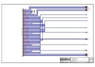
2 Connectors and Configuration<br />
Figure 2.1: Top View<br />
1<br />
J1<br />
R10 R11<br />
R12 R13<br />
1<br />
J2<br />
Page 2
3 Connectors<br />
3.1 J1 <strong>NetDCU</strong> Interface<br />
J3 Display Interface<br />
Pin Signal Function<br />
1 GND Signal Ground<br />
2 R1 Red Bit 1<br />
3 R0 Red Bit 0 (LSB)<br />
4 G5 Green Bit 5 (MSB)<br />
5 G4 Green Bit 4<br />
6 G3 Green Bit 3<br />
7 G2 Green Bit 2<br />
8 GND Signal Ground<br />
9 B3 Blue Bit 3<br />
10 B2 Blue Bit 2<br />
11 B1 Blue Bit 1<br />
12 B0 Blue Bit 0 (LSB)<br />
13 G1 Green Bit 1<br />
14 G0 Green Bit 0 (LSB)<br />
15 B5 Blue Bit 5 (MSB)<br />
16 B4 Blue Bit 4<br />
17 GND Signal Ground<br />
18 VEEK Backlight brightness(*)<br />
19 CLP Data clock pulse<br />
Page 3
J3 Display Interface<br />
Pin Signal Function<br />
20 FRP Frame Impulse<br />
21 M Display data valid signal<br />
22 LIP Line Impulse<br />
23 DEN Display ON<br />
24 GND Signal Ground<br />
25 VLCD Power supply LCD 3.3V<br />
26 -- NC<br />
27 -- NC<br />
28 GND Signal Ground<br />
29 -- NC<br />
30 VCFL Max. +8V for backlight switching<br />
31 R2 Red Bit 2<br />
32 R3 Red Bit 3<br />
33 R4 Red Bit 4<br />
34 R5 Red Bit 5 (MSB)<br />
(*) software adjustable output voltage 0V...+3,3V.<br />
Page 4
3.2 J2 Display Interface<br />
J3 Display Interface<br />
Pin Signal Function<br />
1 GND Signal Ground<br />
2 CLP Data clock pulse<br />
3 LIP Line Impulse<br />
4 FRP Frame Impulse<br />
5 GND Signal Ground<br />
6 R0 Red Bit 0 (LSB)<br />
7 R1 Red Bit 1<br />
8 R2 Red Bit 2<br />
9 R3 Red Bit 3<br />
10 R4 Red Bit 4<br />
11 R5 Red Bit 5 (MSB)<br />
12 GND Signal Ground<br />
13 G0 Green Bit 0 (LSB)<br />
14 G1 Green Bit 1<br />
15 G2 Green Bit 2<br />
16 G3 Green Bit 3<br />
17 G4 Green Bit 4<br />
18 G5 Green Bit 5 (MSB)<br />
19 GND Signal Ground<br />
20 B0 Blue Bit 0 (LSB)<br />
21 B1 Blue Bit 1<br />
Page 5
J3 Display Interface<br />
Pin Signal Function<br />
22 B2 Blue Bit 2<br />
23 B3 Blue Bit 3<br />
24 B4 Blue Bit 4<br />
25 B5 Blue Bit 5 (MSB)<br />
26 GND Signal Ground<br />
27 M Display data valid signal<br />
28 VLCD Power supply LCD 3.3V<br />
29 VLCD Power supply LCD 3.3V<br />
30 CFG1 Configuration Pin<br />
31 CFG2 Configuration Pin<br />
32 -- NC<br />
33 C1 Backlight 1 Cathode<br />
34 C2 Backlight 2 Cathode<br />
35 C3 Backlight 3 Cathode<br />
36 -- NC<br />
37 A1 Backlight 1 Anode<br />
38 A2 Backlight 1 Anode<br />
39 A3 Backlight 1 Anode<br />
40 -- NC<br />
Page 6
4 Configuration <strong>NetDCU</strong>/<strong>ADP</strong>-<strong>TCG057</strong>-L<br />
4.1 Configuration Display Interface Pin 30<br />
Configuration R10 R11<br />
High Level (VCC) x<br />
Low Level (GND) x<br />
Rxx Jumper, 0Ω Resistor Type 1206<br />
4.2 Configuration Display Interface Pin 31<br />
Configuration R12 R13<br />
High Level (VCC) x<br />
Low Level (GND) x<br />
Rxx Jumper, 0Ω Resistor Type 1206<br />
Page 7
5 Dimensions <strong>NetDCU</strong>/<strong>ADP</strong>-<strong>TCG057</strong>-L<br />
Figure 5.1 Top View<br />
Page 8
Index<br />
Configuration.........................................................................5<br />
Display Interface Pin 30.......................................................5<br />
Display Interface Pin 31.......................................................5<br />
Connector<br />
Arrangement........................................................................1<br />
Counting..............................................................................2<br />
Connectors............................................................................2<br />
Dimensions............................................................................6