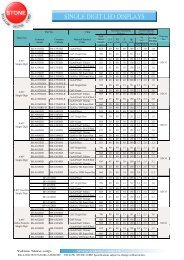
TDA2822 - Tehnari.ru
TDA2822 - Tehnari.ru
TDA2822 - Tehnari.ru

Create successful ePaper yourself
Turn your PDF publications into a flip-book with our unique Google optimized e-Paper software.
®<br />
.<br />
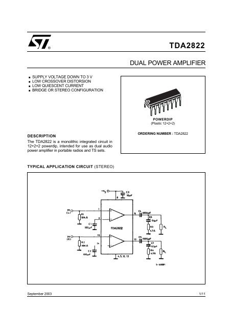
SUPPLY VOLTAGE DOWN TO 3 V<br />
.<br />
LOW CROSSOVER DISTORSION<br />
LOW QUIESCENT CURRENT<br />
BRIDGE OR STEREO CONFIGURATION<br />
DESCRIPTION<br />
The <strong>TDA2822</strong> is a monolithic integrated circuit in<br />
12+2+2 powerdip, intended for use as dual audio<br />
power amplifier in portable radios and TS sets.<br />
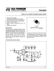
TYPICAL APPLICATION CIRCUIT (STEREO)<br />
September 2003<br />
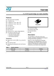
<strong>TDA2822</strong><br />
DUAL POWER AMPLIFIER<br />
POWERDIP<br />
(Plastic 12+2+2)<br />
ORDERING NUMBER : <strong>TDA2822</strong><br />
1/11
<strong>TDA2822</strong><br />
PIN CONNECTION (top view)<br />
SCHEMATIC DIAGRAM<br />
INPUT+(1)<br />
N.C.<br />
INPUT-(1)<br />
GND<br />
GND<br />
OUTPUT(1)<br />
N.C.<br />
ABSOLUTE MAXIMUM RATINGS<br />
1<br />
2<br />
3<br />
4<br />
5<br />
6<br />
GND<br />
GND<br />
7 10 N.C.<br />
INPUT+(2)<br />
INPUT-(2)<br />
OUTPUT(2)<br />
Symbol Parameter Value Unit<br />
Vs Supply Voltage 15 V<br />
Io Output Peak Current 1.5 A<br />
Ptot Total Power Dissipation at Tamb = 50 °C<br />
1.25<br />
W<br />
at Tcase = 70 °C<br />
4<br />
W<br />
Tstg, Tj Storage and Junction Temperature – 40 to 150 °C<br />
2/11<br />
D95AU321<br />
16<br />
15<br />
14<br />
13<br />
12<br />
11<br />
N.C.<br />
+VS 8 9 N.C.
THERMAL DATA<br />
Symbol Parameter Value Unit<br />
Rth j-amb<br />
Rth j-case<br />
Thermal Resistance Junction-ambient<br />
Thermal Resistance Junction-pins<br />
Max<br />
Max<br />
ELECTRICAL CHARACTERISTICS (Vs = 6 V, Tamb = 25 °C, unless otherwise specified)<br />
STEREO (test circuit of fig. 1)<br />
80<br />
20<br />
°C/W<br />
°C/W<br />
Symbol Parameter Test Condition Min. Typ. Max. Unit<br />
Vs Supply Voltage 3 15 V<br />
Vc Quiescent Output Voltage Vs = 9 V<br />
4<br />
V<br />
Vs = 6 V<br />
2.7<br />
V<br />
Id Quiescent Drain Current 6 12 mA<br />
Ib Input Bias Current 100 nA<br />
Po Output Power<br />
d = 10 % f = 1 kHz<br />
(each channel)<br />
Vs = 9 V RL = 4 Ω<br />
1.3 1.7<br />
W<br />
Vs = 6 V RL = 4 Ω<br />
0.45 0.65<br />
W<br />
Vs = 4.5 V RL = 4 Ω<br />
0.32<br />
W<br />
Gv Closed Loop Voltage Gain f = 1 kHz 36 39 41 dB<br />
Ri Input Resistance f = 1 kHz 100 kΩ<br />
e N Total Input Noise Rs = 10 kΩ<br />
B = 22 Hz to 22 kHz<br />
Curve A<br />
SVR Supply Voltage Rejection f = 100 Hz 24 30 dB<br />
CS Channel Separation Rg = 10 kΩ f = 1 kHz 50 dB<br />
Vs Supply Voltage 3 15 V<br />
Id Quiescent Drain Current RL = ∞ 6 12 mA<br />
Vos Output Offset Voltage RL = 8 Ω 10 60 mV<br />
Ib Input Bias Current 100 nA<br />
Po Output Power d = 10 % f = 1 kHz<br />
Vs = 9 V RL = 8 Ω<br />
2.7 3.2<br />
W<br />
Vs = 6 V RL = 8 Ω<br />
0.9 1.35<br />
W<br />
Vs = 4.5 V RL = 4 Ω<br />
1<br />
W<br />
d Distortion (f = 1 kHz) RL = 8 Ω Po = 0.5 W 0.2 %<br />
Gv Closed Loop Voltage Gain f = 1 kHz 39 dB<br />
Ri Input Resistance f = 1 kHz 100 kΩ<br />
e N Total Input Noise Rs = 10 kΩ<br />
B = 22 Hz to 22 kHz<br />
Curve A<br />
2.5<br />
2<br />
3<br />
2.5<br />
<strong>TDA2822</strong><br />
SVR Supply Voltage Rejection f = 100 Hz 40 dB<br />
μV<br />
μV<br />
μV<br />
μV<br />
3/11
<strong>TDA2822</strong><br />
Figure 1 : Test Circuit (stereo).<br />
Figure 2 : P.C. Board and Components Layout of the Circuit of Figure 1 (1:1 scale).<br />
4/11
Figure 3 : Test Circuit (bridge).<br />
Figure 4 : P.C. Board and Components Layout of the Circuit of Figure 3 (1:1 scale).<br />
<strong>TDA2822</strong><br />
5/11
<strong>TDA2822</strong><br />
Figure 5 : Output Power vs. Supply Voltage<br />
(Stereo).<br />
Figure 6 : Output Power vs. Supply Voltage<br />
(Bridge).<br />
Figure 7 : Distorsion vs. Output Power (Bridge). Figure 8 : Distorsion vs. Output Power (Bridge).<br />
Figure 9 : Supply Voltage Rejection vs.<br />
Frequency.<br />
6/11<br />
Figure 10 : Quiescent Current vs. Supply Voltage.
Figure 11 : Total Power Dissipation vs. Output<br />
Power (Stereo).<br />
Figure 13 : Total Power Dissipation vs. Output<br />
Power (Bridge).<br />
<strong>TDA2822</strong><br />
Figure 12 : Total Power Dissipation vs. Output<br />
Power (Bridge).<br />
7/11
<strong>TDA2822</strong><br />
Figure 14 : Application Circuit for Portable Radios.<br />
MOUNTING INSTRUCTION<br />
The Rth j-amb of the <strong>TDA2822</strong> can be reduced by soldering<br />
the GND pins to a suitable copper area of the<br />
printed circuit board (Figure 15) or to an external<br />
heatsink (Figure 16).<br />
The diagram of Figure 17 shows the maximum dissipable<br />
power Ptot and the Rth j-amb as a function of<br />
the side "∂" of two equal square copper areas having<br />
a thickness of 35 μ (1.4 mils).<br />
Figure 15 : Example of P.C. Board Copper Area<br />
which is used as Heatsink.<br />
8/11<br />
During soldering the pins temperature must not exceed<br />
260 °C and the soldering time must not be<br />
longer than 12 seconds.<br />
The external heatsink or printed circuit copper area<br />
must be connected to electrical ground.<br />
Figure 16 : External Heatsink Mounting Example.
Figure 6 : Maximum Dissipable Power and<br />
Junction to Ambient Thermal<br />
Resistance vs. Side "∂".<br />
<strong>TDA2822</strong><br />
Figure 7 : Maximum Allowable Power Dissipation<br />
vs. Ambient Temperature.<br />
9/11
<strong>TDA2822</strong><br />
DIM.<br />
10/11<br />
mm inch<br />
MIN. TYP. MAX. MIN. TYP. MAX.<br />
a1 0.51 0.020<br />
B 0.85 1.40 0.033 0.055<br />
b 0.50 0.020<br />
b1 0.38 0.50 0.015 0.020<br />
D 20.0 0.787<br />
E 8.80 0.346<br />
e 2.54 0.100<br />
e3 17.78 0.700<br />
F 7.10 0.280<br />
I 5.10 0.201<br />
L 3.30 0.130<br />
Z 1.27 0.050<br />
OUTLINE AND<br />
MECHANICAL DATA<br />
Powerdip 16
Information furnished is believed to be accurate and reliable. However, STMicroelectronics assumes no responsibility for the consequences<br />
of use of such information nor for any infringement of patents or other rights of third parties which may result from its use. No<br />
license is granted by implication or otherwise under any patent or patent rights of STMicroelectronics. Specifications mentioned in this<br />
publication are subject to change without notice. This publication supersedes and replaces all information previously supplied. STMicroelectronics<br />
products are not authorized for use as critical components in life support devices or systems without express written<br />
approval of STMicroelectronics.<br />
The ST logo is a registered trademark of STMicroelectronics.<br />
All other names are the property of their respective owners<br />
© 2003 STMicroelectronics - All rights reserved<br />
<strong>TDA2822</strong><br />
STMicroelectronics GROUP OF COMPANIES<br />
Australia – Belgium - Brazil - Canada - China – Czech Republic - Finland - France - Germany - Hong Kong - India - Israel - Italy - Japan -<br />
Malaysia - Malta - Morocco - Singapore - Spain - Sweden - Switzerland - United Kingdom - United States<br />
www.st.com<br />
11/11